Minimum Configuration Insensitive Multifunctional
Current-Mode Biquad Using Current Conveyors
and All-Grounded Passive Components
Wang Chunhua
1, Ali Umit Keskin
2, Leng Yang
1, Zhang Qiujing
1, Du Sichun
11 School of Computer and Communications, Hunan University, Changsha, 410082, China 2 Department of Biomedical Engineering, Yeditepe University, 34755 Istanbul, Turkey [email protected], [email protected], [email protected], [email protected] Abstract. This paper proposes a new current
conveyor-based high-output impedance single-input three-output current mode filter with minimum configuration. It contains two dual output second generation current conveyors, one third generation dual output current conveyor, and four grounded resistors and capacitors. The circuit simultane-ously provides low-pass, band-pass, and high-pass filtering outputs, without any passive component matching condi-tions and restriccondi-tions on input signals. Additionally, the proposed circuit offers following advantages: Minimum active and passive element count, high output and low input impedances, suitable for cascading identical current-mode sections, all passive elements are grounded (no virtual grounding), low natural frequency and Q-factor sensitivities. The influences of non-ideal current conveyors on the proposed circuit are researched in the last.
Keywords
Current conveyor, current-mode circuit, filter, parasitic impedance.
1.
Introduction
Second generation current conveyor (CCII) element which has a single current output terminal is one of the versatile active building blocks to construct continuous-time universal and multipurpose filters, and many of these filters have already been reported in literature [1-3]. CCII can not provide feedforward and feedback currents at the same time, and CCII-based filters become rather complex. Modified current conveyors, such as MOCCII (current conveyor with multi-output terminals) [4-5] and DOCCII (second generation current conveyors with dual output terminals) [6-8] are employed to produce filters. Although the MOCCII-based filters have simple structure, their current tracking errors will increase proportionally with the number of current output terminals. On the other hand, DOCCII has two current output terminals (one positive, another negative), its current tracking errors are relatively small, and it has a balanced output structure.
Many different current mode filter topologies can be realized by employing second generation current conveyors with dual output terminals [6–16]. Structurally, DOCCII based filters and their variants can be divided into three classes: (i) multi-input and multi-output (MIMO) filters [6]; (ii) multi-input and single-output filters [7-9]; (iii) sin-gle-input and three-output (SITO) filters [10-16]. The SITO filters can realize second order low-pass (LP), band-pass (BP), high-pass (HP) filters simultaneously without any passive component matching conditions and restrictions on input signals. These filters also allow the realizations of notch and all-pass (AP) filter responses without having to change the filter configurations.
Soliman proposes current mode filter circuit with high-output impedance using three DOCCII and five grounded RC elements [10], the filter’s natural frequency and quality factor can be adjusted independently. However, the circuit only produces two-outputs (low-pass and band-pass). In another study, Soliman gives several dual and three outputs CM filter configurations with high impedance outputs [11].
Abuelma’atti et al. propose SITO current mode filter circuit with high-output impedance using three DOCCIIs, one OTA (operational transconductance amplifier) and five grounded RC elements [12]. Gunes et al. describe a SITO current mode filter circuit employing three DOCCIIs and four grounded RC components [13]. However, the band-pass and high-band-pass outputs of this circuit do not provide high-output impedances. Toker et al. present a SITO cur-rent mode filter circuit with high-output impedance using three DOCCIIs, five grounded RC elements [14]. Toker et al. proposed another SITO filter circuit for low frequency operation in [15]. The circuit includes four DOCCIIs and eight passive elements. Cicekoglu introduces five SITO current mode filter circuits, each of them containing four DOCCII and seven RC components with high-output impedances [16]. Keskin and Cam propose a new SITO current mode filter circuit with high-output impedance using three DOCCIIs and four passive elements [17]. Although it is a minimum configuration structure, there is one virtually grounded resistor in addition to three grounded passive components in their circuit. The CM DOCCII-based filter introduced by Ikeda and Tomita [18]
has three active and four passive elements, but does not provide simultaneous outputs. While the works in [19], [20] describe minimum configuration circuits with high impedance outputs, both of them contain floating capacitors.
Tangsrirat et al. propose a two-input three-output current-mode filter, which employs three dual-output current-controlled current conveyors (DOCCCIIs) and two grounded capacitors [21]. In another study, Tangsrirat demonstrates a CM filter with two inputs and two outputs employing four DOCCCIIs and two grounded capacitors [22]. However, neither of these circuits belongs to SITO topology.
Singh et al. show how a four current conveyor based voltage mode biquad filter with five resistors and two grounded capacitors provides also current mode capability [23].
So far (to the best knowledge of authors), there exists no study on DOCCII-based CM SITO filters offering mini-mum filter configurations accompanied with all-grounded passive component structure with high impedance outputs.
On the other hand, third generation current conveyor (CCIII) is proposed by Fabre [24], and a CMOS implemen-tation of this circuit is presented in [25]. DOCCIII (third generation current conveyor with two current outputs) can easily be constructed in a CMOS technology. Numerous applications of CCIII element have already been presented in literature [26-30].
In this paper, a new current mode SITO type mini-mum configuration filter is proposed. This circuit consists of one third generation current conveyor and two second generation current conveyors in addition to four grounded passive elements.
2.
The Proposed Circuit
The symbolic notations of DOCCII and DOCCIII four terminal active elements are shown in Fig. 1.a, b. DOCCII is characterized by x z x z y y x V I I I I I V , 0, , . (1)
On the other hand, third generation current conveyor with dual outputs, DOCCIII is described by
x z x z x y y x V I I I I I I V , , , . (2)
(a)DOCCII (b) DOCCIII
Fig.1. Circuit symbols of DOCCII and DOCCIII.
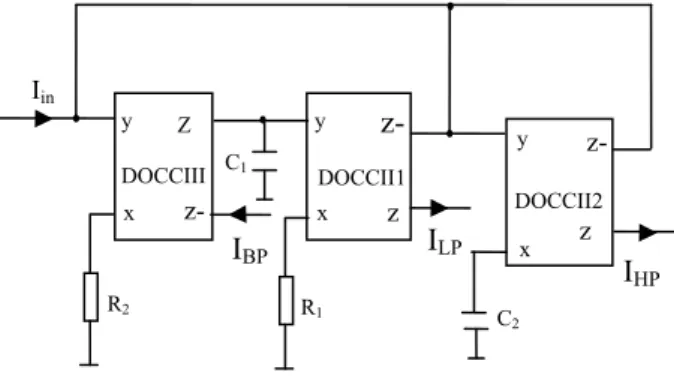
The proposed circuit is shown in Fig. 2. The circuit contains two DOCCIIs, one DOCCIII, two grounded resistors and grounded capacitors, and it can realize low-pass, band-pass and high-pass filters simultaneously, at high impedance outputs. From Fig. 2, the input terminal of circuit is terminal Y of DOCCIII, so according to (2) (namely: Vx = Vy, Iy = -Ix), it is clear that the circuit has low input impedance. It is convenient for the circuit to be cascaded for its high output impedance and low input impedance.
Fig. 2. Proposed SITO current mode filtering circuit.
The filter provides the following transfer functions simultaneously: 1 1 1 1 2 1 2 1 2 C sR C C R R s I I in LP , (3) 1 1 1 2 1 2 1 2 1 1 C sR C C R R s C sR I I in BP , (4) 1 1 1 2 1 2 1 2 2 1 1 2 2 C sR C C R R s C C R R s I I in HP . (5)
The band-stop (BS) filtering output can be obtained by connecting low-pass and high-pass outputs (ILP+IHP), and all-pass (AP) filtering output can be obtained by connecting low-pass, band-pass and high-pass outputs (ILP-IBP+IHP) together as depicted in (6), (7). Therefore, the proposed circuit can be easily transformed into a universal filter. 1 1 1 1 2 1 2 1 2 2 1 1 2 2 C sR C C R R s C C R R s I I I I I in HP LP in BS , (6) 1 1 1 1 2 1 2 1 2 1 1 2 1 1 2 2 C sR C C R R s C sR C C R R s I I I I I I in BP HP LP in AP . (7)
The natural angular frequency and quality factor are given in (8a, 8b), respectively.
2 1 2 1 0 1 C C R R
, (8a) 1 1 2 2 C R C R Q . (8b)Ideal passive 0 and Q sensitivities are both 1/2 in magnitude. Iy Ix IZ+ I Z-y z DOCCII x z-Vy Vx Vz Vz- x z-y z Vz Vy Vx V z-Iy Ix IZ+ IZ- DOCCIII z y x Z z- DOCCIII DOCCII1 z-DOCCII2 Iin ILP C1 C2 R1 R2 IBP x y y x z- z IHP
Taking the non-idealities of the DOCCII and DOCCIII into account, their terminal relationships can be rewritten respectively as follows:
x z x z y y x V I I I I I V , 0, , , (9) x z x z x y y x V I I I I I I V , , , (10)
where and are current gains and is voltage gain, and
= 1−iz , = 1−ix, = 1−v. Here, iz, ix, v are current- and voltage-tracking errors of the DOCCII and DOCCIII.
Considering these non-idealities of the DOCCII and DOCCIII, current transfer functions in Fig. 2 become:
) ( ) ( ) ( ) ( , ) ( 1 1 1 1 1 2 1 2 1 2 1 1 1 1 s D C C R R s I I s D C sR I I s D I I in HP in BP in LP
(11) where 1 ) ( ) ( ) ( 1 1 1 1 1 1 2 2 2 1 2 1 2
C R s C C R R s s D(12)
In (11), (12); , and are parameters of DOCCIII, and i, i are parameters of DOCCIIi (i=1,2).
The natural angular frequency and quality factor are
1 1 2 1 2 1 2 2 2 2 2 1 2 1 1 1 0 1 , C R C R Q C C R R
.
(13)Active sensitivities of the natural angular frequency and the quality factor of the filter shown in Fig. 2 are
2 1 0 2 , 2 0 1 , , 1 ,
S
S
, 0 0 S
(14) 2 1 2 , 1 , , 2 , 1 , Q QS
S
,S
Q 1 . (15)It is clearly observed that active sensitivities of 0 and Q do not exceed unity.
3.
Results of Circuit Simulations
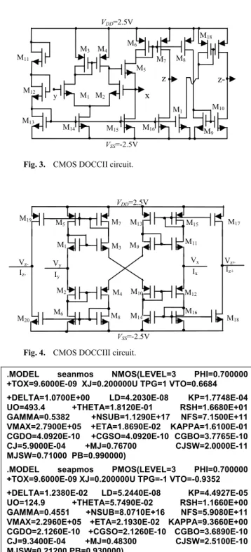
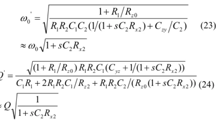
In order to confirm the practical validity of the pro-posed SITO filter circuit, it is simulated in SPICE using 0.5µm CMOS process parameters for transistors shown in Tab. 1. The CMOS DOCCII [31] given in Fig. 3, and CMOS DOCCIII [25] of Fig. 4 are used in circuit simula-tions. Tab. 2 lists the transistor dimensions used in two circuits.
Fig. 5 displays the results of circuit simulations for the proposed multifunction filter. Fig. 6 denotes the simula-tions results of phase and gain for all-pass filtering output.
Fig. 3. CMOS DOCCII circuit.
Fig. 4. CMOS DOCCIII circuit.
.MODEL seanmos NMOS(LEVEL=3 PHI=0.700000 +TOX=9.6000E-09 XJ=0.200000U TPG=1 VTO=0.6684
+DELTA=1.0700E+00 LD=4.2030E-08 KP=1.7748E-04 UO=493.4 +THETA=1.8120E-01 RSH=1.6680E+01 GAMMA=0.5382 +NSUB=1.1290E+17 NFS=7.1500E+11 VMAX=2.7900E+05 +ETA=1.8690E-02 KAPPA=1.6100E-01 CGDO=4.0920E-10 +CGSO=4.0920E-10 CGBO=3.7765E-10 CJ=5.9000E-04 +MJ=0.76700 CJSW=2.0000E-11 MJSW=0.71000 PB=0.990000)
.MODEL seapmos PMOS(LEVEL=3 PHI=0.700000 +TOX=9.6000E-09 XJ=0.200000U TPG=-1 VTO=-0.9352
+DELTA=1.2380E-02 LD=5.2440E-08 KP=4.4927E-05 UO=124.9 +THETA=5.7490E-02 RSH=1.1660E+00 GAMMA=0.4551 +NSUB=8.0710E+16 NFS=5.9080E+11 VMAX=2.2960E+05 +ETA=2.1930E-02 KAPPA=9.3660E+00 CGDO=2.1260E-10 +CGSO=2.1260E-10 CGBO=3.6890E-10 CJ=9.3400E-04 +MJ=0.48300 CJSW=2.5100E-10 MJSW=0.21200 PB=0.930000)
Tab. 1. 0.5µm CMOS process parameters for transistors.
DOCCII M1~ M4 M5~ M10 M11 M12 M13 M14 M15~ M17 M18 M19 W/L(um) 8/2 10/2 4/2 12/2 19/2 8/2 4/2 DOCCIII M1 M3 M6 M8 M9 M11 M14 M16 M18 M20 M2 M4 M5 M10 M12 M13 M15 M17 M19 W/L(um) 4/2 16/2
Tab. 2. Transistor dimensions in the DOCCII and DOCCIII circuits. M1 M2 M3 M4 M5 M6 M7 M8 M9 M10 M13 M14 M19 M20 Vy Vx V z-Iz- Iy Ix M17 M18 Vz+ Iz+ VDD=2.5V VSS=-2.5V M15 M11 M12 M16 M6 M1 M2 M3 M4 M11 M5 y x VDD=2.5V VSS=-2.5V M13 M14 M15 M16 M10 M18 M8 M9 z M1 z-M7 M12
Fig. 5. Results of circuit simulations for basic filter responses of the proposed DOCCII-based SITO biquad.
Fig. 6. Frequency responses characteristic of the AP filter.
Fig. 7. Input impedance of the filter.
The input and output impedance of CFBCCII can be seen in Fig. 7 and Fig. 8. Here, component values are selected as R1= R2= 5 kΩ, and C1= C2= 1 nF, which yield
f0 = 34 kHz and Q = 1. Fig. 9 shows the simulated band-pass responses with Q-tuning (i.e. Q = 1, 4, 6). In this case,
R1= 5 kΩ, 1.25 kΩ, 0.84 kΩ and R2= 5 kΩ, 20 kΩ, 30 kΩ and C1= C2= 1 nF respectively while keeping ω0 invariant. Supply voltages are ±2.5 V. It is noted that the results of circuit simulations are in agreement with theory. For the band-pass filter, the simulated curve departs from ideal beginning at about 10 MHz, due to the parasitic
impedances of DOCCII and DOCCIII. This behavior is further analyzed in the following section.
Note that, since the aim of this study is to design a minimum configuration CM-SITO filter, independent control of frequency or quality factor is not expected.
Fig. 8. Output impedance of the filter.
Fig. 9. Simulation results of frequency response of BP filter with different Q (keeping ω0 invariant).
4.
Parasitic Impedance Influence
of DOCCII and DOCCIII
The non-ideal CCII [32] and CCIII models are shown in Fig. 10. The real CCII and CCIII has parasitic resistors and capacitors at terminal z to the ground, and a serial resistor at the input terminal x. In the CCII, parasitic resistors and capacitors exist at terminal y to the ground [32]. A series parasitic resistor exists at the terminal y of the CCIII. Here, α(s) and β(s) are used to represent the frequency domain transfer functions of the internal current and voltage followers of the CCII and CCIII, respectively, and they are considered as having unity values here.
(a) CCII (b) CCIII
Fig. 10. Non-ideal CCII and CCIII with their parasitic resistors and capacitors. 1 10 102 103 104 105 106 107 Frequency(Hz) -50 -40 -20 10 0 Q=1 Q=4 Q=6 Ga in (d B) y' z' Cy Ry y x' α(s) Cz Rz β(s) z Rx CCII y' z' Ry y x' Cz Rz β(s) z Rx CCIII 1 10 102 103 104 105 106 107 108 109 Frequency (Hz) -70 -40 -20 -60 0 10 Ga in (d B) LP HP BP BS 4.0 3.0 1.0 2.0 1 10 102 103 104 105 106 107 108 Frequency(Hz) Ou tp ut im pe da nc e (M Ω ) LP BP HP 40 00 -1000 -2000 -3000 -4000 0 103 104 105 106 107 Frequency (Hz) Phase Theoretical Simulated Gain Theoretical Simulated PhaseGain(dB) -1 -0.5 0.5 1 1 10 102 103 104 105 106 107 108 Frequency (Hz) In pu t i m pe da nc e ( Ω ) 1.0M 1.0G 100T 1.0T
In a non-ideal DOCCII and DOCCIII, parasitic resistors and capacitors at the z+, z- terminals are assumed to have the same values, all being equal to Rz and Cz respectively.
In order to study the influence of parasitic elements in DOCCII and DOCCIII, the proposed filter shown in Fig. 2 can be transformed to Fig. 11.
We define Rz1, Rz2, Cz1, Cz2 as the parasitic resistors and capacitors of the z terminals of DOCCII1 and DOCCII2 in Fig. 11, and Rz0, Cz0 at the z terminal of DOCCIII. Rx1,Rx2 are the serial parasitic resistances at the x terminals of DOCCII1 and DOCCII2, Rx0 is the parasitic resistance for DOCCIII, while Ry1, Ry2, Cy1, Cy2 are the parasitic resistors and capacitors at the y terminals of DOCCII1 and DOCCII2. Ry0 is the serial parasitic resis-tance of DOCCIII which is equal to Rx0 approximately.
Fig. 11. The proposed filter including the parasitic elements of the DOCCII and DOCCIII.
Assuming that C1>>(Cy1+Cz0), it can be shown that 0 1 0 1 0 0 1 1 1 ) // //( // z z y z z R sC R C C R C Z
,
(16) 2 2 2 2 2 2 1 1 sC R sC sC R Z x x , (17) 1 2 2 ) // // //( ) // ( 2 2 2 2 1 2 1 3 z yz z z y z z z R sC R C C C R R Z (18)where Cyz=Cz1+Cy2+Cz2. From Fig. 11 one can obtain the following transfer functions:
) ( 1 3 2 1 3 2 1 2 2 1 3 2 1 3 2 1 s D Z Z R Z R R Z R R Z Z Z Z Z Z I I in LP , (19) ) ( 3 2 1 3 2 1 3 2 1 2 2 1 3 2 1 3 2 1 s D Z Z R Z Z R Z R R Z R R Z Z Z Z Z R I I in BP
,
(20) ) ( 3 2 1 3 2 1 3 2 1 2 2 1 3 2 1 3 2 1 s D Z R R Z Z R Z R R Z R R Z Z Z Z R R I I in HP (21) where ) 1 ( ) ) 1 ( 2 ( ) 1 ( ( ) ( 0 1 2 2 0 2 2 1 2 1 2 1 1 1 2 2 2 1 2 1 2 z x z z x yz R R R sC R C R R R C R R R C s R sC C C C R R s s D (22)
For the value of Cyzis smaller than 10 pF and that of Rz0, Rz2 is larger than 1 MΩ, so C1, C2, R1, R2 are chosen under the following relations: Cyz << min(C1, C2),
min(Rz0,Rz0) >> max(R1, R2). Therefore ,
2 2 0 2 2 2 2 1 2 1 0 1 ' 0 1 ) ) 1 ( 1 ( 1 x zy x z R sC C C R sC C C R R R R
(23) 2 2 2 2 0 2 2 1 2 1 2 1 1 1 2 2 1 2 1 0 1 ' 1 1 )) 1 ( ( 2 )) 1 ( 1 ( ) 1 ( x x z z x yz z R sC Q R sC R C R R R C R R R C R sC C C R R R R Q (24)
From (23) and (24), it is clear that when considering influence of parasitic elements, the natural angular fre-quency is larger than the one in ideal condition, namely
ω0’ > ω0, and the quality factor is lower than that of the
ideal one (Q` < Q). If ωC2Rx2 << 1, the influence of non-ideal characteristics of DOCCII can be ignored. Note that the value of Rx is low, as given below [32].
m1 m2 d2 d4 m1 m2 m5 40
x g g g g g g g
R .(25)
The influence of parasitic elements on the proposed filter is simulated by PSPICE. It can be seen in Fig. 12 that in the proposed filter, the parasitic elements have some influences on the ω0and Q of the proposed filter. In this case, C1 = C2 = 0.25 nF, 1 nF, 5 nF, 10 nF and
R1= R2= 20 kΩ, 5 kΩ, 1 kΩ, 0.5 kΩ, respectively. Supply voltages are ±2.5 V. When ωC2Rx2 << 1 (e.g. C2= 0.25 nF as shown in Fig. 11), the DOCCII can be seen as the ideal one. Therefore, the simulation results are in good agree-ment with the theoretical analysis.
Fig. 12. Simulation results of the influence of parasitic elements on the proposed filter.
5.
Conclusions
In this work, a new current mode SITO biquad is presented. This filter employs minimum number of active and passive elements. The proposed current mode filter can
10 0 -80 -40 -100 1 10 102 103 104 105 106 107 108 109 Frequency(Hz Ga in (d B) C2=0.25nF C2=1nF C2=5nF C2=10nF y x z z- DOCCIII y x z-z DOCCII1 y x z- z DOCCII2 Iin IBP ILP IHP Z1 R1 R2 Z2 Z3
be easily cascaded, since it realizes three simultaneous filter functions at high impedance outputs, while its input impedance is low. In this filter, AP and notch responses can also be obtained by interconnecting the corresponding outputs. Moreover, all passive components are grounded, and its frequency and Q-factor sensitivities are low.
Acknowledgements
The authors would like to thank the National Natural Science Foundation of China for financially supporting this research under grant No. 60676021.
References
[1] HIGASHIMURA, M., FUKUI, Y. Universal filter using plus-type CCIIs. Electronics Letters, 1996, vol. 32, p. 810-811.
[2] SOLIMAN, A. M. Kerwin-Huelsman-Newcomb circuit using current conveyors. Electronics Letters, 1994, vol. 30, no. 24, p. 2019-2020.
[3] CHANG, C. M., CHEN, P. C. Universal active current filter with three inputs and one output using current conveyors. International Journal of Electronics, 1991, vol. 71, no. 5, p. 817-819.
[4] WU, J., MASRY, E. E. Current-mode ladder filters using multiple output current conveyors. IEE Proceeding-G, 1996, vol. 143, no. 4, p. 218-222.
[5] HORNG, J. W., HOU, C. L., CHANG, C. M., et al. Universal current filter with single input and three outputs using MOCCIIs.
Int. Journal of Electronics, 2007, vol. 94, no. 4, p. 327 to 333. [6] SUN, Y, JEFFERIES, B. Current-mode biquadratic filters using
dual output current conveyor. In Proceedings of the of the 5th IEEE
International Conference on Electronic Circuits and Systems.
September 1998, p. 135–8.
[7] GUNES, E. O., TOKER, A., OZOGUZ, S. Insensitive current-mode universal filter with minimum components using dual-output current conveyors. Electronics Letters, 1999, vol. 35, no. 7, p. 524 to 525.
[8] SIRIPRUCHYANUN, M., JAIKLA, W. Three-input single-output electronically controllable dual-mode universal biquad filter using DO-CCCIIs. The Journal of KMITNB., 2007, vol. 17, no. 1. [9] JAIKLA, W., SILAPAN, P., SIRIPRUCHYANUN, M.
Low-component electronically controllable dual-mode universal biquad filter using DO-CCCIIs. In Int. Symposium on Communications and Information Technologies (ISCIT 2007).
[10] SOLIMAN, A. M. Current mode universal filter. Electronics Letters, 1995, vol. 31, p. 1420–1.
[11] SOLIMAN, A. M. New current mode filters using current conveyors. AEÜ Int J. Electron. Commun., 1997, vol. 51, no. 5, p. 275-278.
[12] ABUELMA’ATTI, M. T, KHAN, M. H. Low component current-mode universal filter. Electronics Letters, 1995, vol. 31, p. 216-1. [13] GUNES, E. O, ANDAY, F. Realization of universal current mode
filters using CFCCIIs. Electronics Letters, 1996, vol. 36, p. 1081 to 1082.
[14] TOKER, A, OZOGUZ, S. Insensitive current-mode universal filter using dual output current conveyors. Int J Electron., 2000, vol. 87, p. 667–74.
[15] TOKER, A, OZOGUZ, S. Integrable current-mode filter realization using dual-output current conveyors for low-frequency operation. AEU Int J Electron Commun, 2001, vol. 55, p. 145–9. [16] CICEKOGLU, O., TARIM, N., KUNTMAN, H. Wide dynamic
range high output impedance current-mode multifunction filters with dual-output current conveyors. AEU- Int J Electron Commun., 2002, vol. 56, p. 55–60.
[17] KESKIN, A. U., CAM, U. Insensitive high-output impedance minimum configuration SITO-type current-mode biquad using dual-output current conveyors and grounded passive components. AEU- Int. J. Electron. Commun., 2007, vol. 61, p. 341 – 344. [18] IKEDA, K., TOMITA, Y. Realization of current-mode biquadratic
filter using CCIIs with current followers. Electron. Commun. Jpn., Part. 2, Electron., 1994, vol. 77, p. 99-107.
[19] TOKER, A., ÖZOGUZ, S., ÇIÇEKOGLU, O. High output impedance current-mode multifunction filters with minimum number of active and passive elements using dual-output current conveyors. Frequenz, 1999, vol. 53, p. 206-209.
[20] TOKER, A., ÖZOGUZ, S., ÇIÇEKOGLU, O. A new current-mode multifunction filter with minimum components using dual-output current conveyors. In Proc. of ITC-CSCC'99, 1999, vol. I, p. 301-303.
[21] TANGSRIRAT, W., SURAKAMPONTORN, W. High output impedance current-mode universal filter employing dual-output current-controlled conveyors and grounded capacitors. AEU-Int J. Electron. Commun,, 2007, vol. 61, no. 2, p. 127-131.
[22] TANGSRIRAT, W. Current-tunable current-mode multifunction filter based on dual-output current-controlled conveyors. AEU-Int J. Electron. Commun,, 2007, vol. 61,no. 8, p. 528-533.
[23] SINGH, V. K., SINGH, A. K., SENANI, R. Dual function capability of recently proposed four-current-conveyor-based VM biquad. Journal of Circuits, Systems, and Computers, 2005, vol. 14, no. 1, p. 51–56.
[24] FABRE, A. Third-generation current conveyor: A new helpful active element. Electron. Lett., 1995, vol. 31, no. 5, p. 338 to 339. [25] PIOVACCARI, A. CMOS integrated third-generation current
conveyor. Electronics Letters, 1995, vol. 31,no. 105, p. 1228 -9. [26] SUDANSHU, M., IQBAL, A. K. Novel first order allpass section
using single CCIII. Int. Journal of Electronics, 2001, vol. 88, p. 773-778.
[27] WANG, H. Y., LEE, C. T. Systematic synthesis R-L and C-D immitances using single CCIII. Electronics Letters, 2000, vol. 87, p. 293-294.
[28] AHMET, M. T., KHAN, I. A., MİNHEJ, N. On transconductance quadrature oscillators. Int. Journal of Electronics, 1997, vol. 83, no. 2, p. 201-207.
[29] UN, M., KACAR, F. Third generation current conveyor based current-mode fırst order all-pass fılter and quadrature oscıllator.
Journal of Electrical & Electronics Engineering, 2008, vol. 8, no. 1, p. 529-535.
[30] LATTENBERG, I., VRBA, K., DOSTÁL, T. Bipolar CCIII+ and CCIII- conveyors and their current mode-filter application. In
Proc. of the Fourth IEEE International Caracas Conference on Devices, Circuits and Systems. Aruba, ICCDCS Publications. 2002, p. 1 - 4. ISBN 0-7803-7381-2.
[31] SURAKAMPONTORN, W, KIEWRUJA, V, KUMWACHARA, K, et al. Accurate CMOS-based current conveyors. IEEE Trans. on Instrumentation and Measurement, 1991, vol. 40, no. 4, p. 699 to 702.
[32] FABRE, A., SAAID, O., BARHELEMY, H. On the frequency limitations of the circuits based on second generation current conveyors. Analog Integrated Circuits and Signal Processing, 1995, vol. 7, no. 2, p. 113-129.
About Authors...
Wang Chunhua was born in Yongzhou, China, in 1963. He received the B.Sc degree from Hengyang Teacher’s College, Hengyang, China, in 1983, the M.Sc degree from Physics Department, Zhengzhou University, Zhengzhou, China, in 1994, the Ph.D. degree from School of Electronic Information and Control Engineering, Beijing University of Technology, Beijing, China, in 2003. He is currently a Professor of School of Computer and Communication, Hunan University, Changsha, China. From 2004 to 2005, he served as a Professor and the associate Dean of Informa-tion Engineering, Xiangtan University, Xiangtan, China. His research interests include current-mode circuit design, filtering, radio frequency circuit and wireless communications.
Ali Umit Keskin was born in Bursa,Turkey. He received his B.SEE. degree from the Bogazici University in 1978, M.SEE. from the Yildiz Technical University (1980) and Ph.D. degree from the Institute of Science and Technology,
Istanbul Technical University (1984). In 1985, he joined Siemens AG, Turkey. He was engaged in the field of Medi-cal Instrumentation throughout his professional career. Now he is affiliated as an Associate Professor in the Fac-ulty of Engineering, Yeditepe University, Istanbul. His main research interests are analog circuits and signal proc-essing, transducers, spectroscopy, medical instrumentation theory and its applications.
Leng Yang was born in Changde, Hunan, China, in 1984. She received the B.S. from Hunan Normal University in 2006. She is studying in Hunan University for master degree now. She is interested in analog IC circuit and filter design.
Zhang Qiujing was born in Jishou, Hunan, China, in 1982. She received the B.S. from School of Computer and Communication, Changsha University of Science and technology. She is studying in Hunan University for her Ph.D. degree now. She is interested in analog IC circuit and filter design.