A Detailed Cost Model for Concurrent Use With
Hardware/Software Co-Design
Daniel Ragan
Elect. Systems Cost Modeling Lab.
University of Maryland
College Park, MD 20742
[email protected]
Peter Sandborn
Elect. Systems Cost Modeling Lab.
University of Maryland
College Park, MD 20742
[email protected]
Paul Stoaks
Foresight-Systems, Inc.
8217 Shoal Creek Blvd, Suite 100
Austin, Texas 78757
[email protected]
ABSTRACT
Hardware/software co-design methodologies generally focus on the prediction of system performance or co-verification of system functionality. This study extends this conventional focus through the development of a methodology and software tool that evaluates system (hardware and software) development, fabrication, and testing costs (dollar costs) concurrent with hardware/software partitioning in a co-design environment.
Based on the determination of key metrics such as gate count and lines of software, a new tool called Ghost, evaluates software and hardware development, fabrication, packaging and testing costs. Ghost enables optimization of hardware/software partitioning as a function of specific combinations of hardware foundries and software development environments.
Categories and Subject Descriptors
E3 [HW/SW co-design]: specification, model., co-simulation and performance analysis, system-level scheduling and partitioning.
General Terms
Design, Economics.Keywords
Cost Modeling, Cost-Performance Trade-off.1. INTRODUCTION
Hardware/software co-design leads to accelerated system design and performance improvement through dynamic trade-off analysis. Co-design has been a popular topic during the past dec-ade in electronics because designers perceive that performance, reliability, size, and cost can be improved through judicious partitioning of functionality between hardware and software.
System requirements include constraints on functionality, performance, task scheduling, packaging, cost, size, weight, volume, power, reliability, and software and hardware modularity. A variety of alternative architectures may exist that meet both functional and performance standards. Meeting constraints while attempting to optimize the design brings about a number of challenges. One significant gap in co-design methodology is the automation of detailed concurrent cost evaluation. In fact, the majority of system design work categorizing itself as
“cost-performance trade-off” is dominated by “cost-performance with either very simplistic or purely qualitative cost treatments.
No matter what methodology is used when making system design decisions, dollar cost is often a dominant factor. While cost can be the easiest to measure, it may be the hardest to predict. This is because there is never a simple bottom line; behind the final system cost are a multiplicity of other cost factors, including software and hardware design, hardware manufacturing, software development, software and hardware testing, time-to-market factors, yield, and a host of life cycle costs including reliability, maintenance, and disposal. Ideally, all of these costs should be visible and considered during system design, and especially when design-partitioning decisions are made.
The next section in this paper discusses existing work on the concurrent evaluation of performance and cost during hardware/software co-design. Section 3 summarizes the cost modeling methodology developed in this work. Section 4 presents a case study of the JPEG encoder in a digital camera.
2. EXISTING
WORK
The majority of existing work on hardware/software co-design focuses on resource utilization (processor, memory, size, power consumption, timing, etc.). Very few studies have attempted to examine the cost impacts of co-design decisions.
In the DARPA RASSP program, DeBardelaben et al [1] developed a design methodology that involved the development of executable specifications, cost-driven architecture selection, task assignment, task scheduling, and performance modeling. For software cost models, they used COCOMO [2] and REVIC [3]. These models allowed the prediction of software development and maintenance effort, and software development schedule. In order to utilize these models, they estimated software size, using a non-linear reuse technique, [4]. For hardware, DeBardelaben et al
assume only COTS hardware is used and thereby hardware production costs were obtained from vendor quotes. In related work by Egolf [5], a more detailed analysis of ASIC design/redesign, and testing costs was developed.
Also in the DARPA RASSP program, PRICE Systems in collaboration with Ascent Logic built a general design requirements capture and tracking tool called RDD-100. This tool was integrated with PRICE’s parametric cost estimating tools. PRICE built software to read the RDD-100 architecture and constructed an integrated hardware/software work breakdown structure of the candidate architecture. Using the work breakdown structure, PRICE returned the cost to RDD-100, where it was assigned to the corresponding architecture blocks.
Other synthesis approaches either factor in only hardware costs, [6]-[9], or only software costs, [10] during the system design Permission to make digital or hard copies of all or part of this work for
personal or classroom use is granted without fee provided that copies are not made or distributed for profit or commercial advantage and that copies bear this notice and the full citation on the first page. To copy otherwise, or republish, to post on servers or to redistribute to lists, requires prior specific permission and/or a fee.
DAC 2002, June 10-14, 2002, New Orleans, Louisiana, USA.
Functional Blocks Feature Points Source Lines of Code (SLOC) Software Development and Testing Cost Calibration Factor Language Conversion Equivalent SLOC including reuse Software development effort Software maintenance effort Software schedule COCOMO (REVIC) Functional Blocks Feature Points Source Lines of Code (SLOC) Software Development and Testing Cost Calibration Factor Language Conversion Equivalent SLOC including reuse Software development effort Software maintenance effort Software schedule COCOMO (REVIC)
Figure 1: Software cost analysis process.
process. In [11], both hardware and software costs are determined from libraries consisting of functional units with their corresponding performance, and dollar costs.
The majority of co-design and synthesis approaches that address dollar cost do not derive a cost, but rather only accumulate the costs of predefined functional units (hardware and/or software) ignoring many critical economic effects such as production volume, testing, development, and yield. The few studies that do include detailed cost modeling, e.g, [1], are more focused on software development costs than non-recurring or recurring hardware costs. In this paper we show how the best partitioning choice can be made based on both performance and detailed cost calculations by presenting a method of incorporating comprehensive hardware and software cost modeling into the architecture selection and partitioning process to minimize system cost while maintaining system performance standards.
3.
COST MODELING APPROACH
In this section, we describe the composition of the software and hardware cost models that are utilized to estimate chip costs and discuss the implementation of the software and hardware cost models in a software tool called Ghost.
3.1
Software Cost Modeling
For costing software development, several tools exist including COCOMO, REVIC and commercial tools. These software cost estimators use nominal effort equations derived from labor effort required for developing software as related to the size of the software system measured in source lines of code or delivered source instructions.
In this study, software size was estimated using a form of function point analysis [12] known as feature point counting [13]. Based on software language, any feature point count can be converted to the number of source lines of code (SLOC) using a conversion factor. One Feature Point is equivalent to 10 to 320 SLOC depending on the language. For this work, the language of interest, Java, is considered a level six language and converts each Feature Point to 53 SLOC, [14]. Once a SLOC count is known, effort and scheduling equations are derived. In particular, the embedded mode of COCOMO and REVIC are the most applicable for the software costing of an embedded digital system,
e.g., the digital camera considered in this paper (Section 4). Adjustments made by DeBardelaben aimed at COTS-based embedded DSP systems were also utilized [15]. The software cost analysis process is summarized in Figure 1.
The converted SLOC counts from the function/feature point counting process are entered into software cost estimating equations based on COCOMO. The methodology developed in this paper computes software size with reuse taken into account, software development effort, software maintenance effort, and the software schedule. The software schedule is based on REVIC development time [4] with the multiplicative effects on time with projects of increasing effort set to 6.2 [15].
The level of accuracy of the estimate provided by this software cost model is proportional to the user’s confidence in the software size estimate and the description of the software development environment. Through calibration, the risks associated with estimating software development have been reduced.
3.2
Hardware Cost Modeling
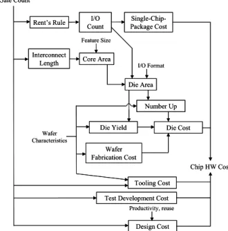
The hardware cost modeling process is shown in Figure 2. The key metric, gate count, allows the calculation of values for I/O count, core area, die size, etc. These factors are coupled with others such as number-up, chip design costs, wafer fabrication, packaging, automatic test pattern generation, and manual test pattern generation, to obtain the final cost.
The number of die I/O is determined using Rent’s rule, which relates the chip functionality and number of gates to the number of signal and control I/O on the die. The core area of the die is determined using Donath’s formulation of average interconnections length from Rent’s rule [16]. Based on the number of gates on the chip, Ng, the average interconnection
length in units of gate pitch, R, can be determined from the interconnection pitch, pw, number of interconnection layers, nw,
utilization efficiency of interconnections, ew, and the fan-out of
gates, fg. Using the average interconnection length, the gate
dimension dg, and the die core dimension Dc, can be obtained by
setting the supply and demand for wiring equal.
I/O Count Die Area Core Area Gate Count Wafer Characteristics Design Cost Tooling Cost Wafer Fabrication Cost Single-Chip-Package Cost Feature Size Interconnect Length Die Yield Number Up Die Cost Chip HW Cost I/O Format Rent’s Rule
Test Development Cost Productivity, reuse I/O Count Die Area Core Area Gate Count Wafer Characteristics Design Cost Tooling Cost Wafer Fabrication Cost Single-Chip-Package Cost Feature Size Interconnect Length Die Yield Number Up Die Cost Chip HW Cost I/O Format Rent’s Rule
Test Development Cost Productivity, reuse
w w w g g e n p R f d = and Dc = Ngdg (1)
For peripherally bonded die with a single row of bond pads on all sides, the die area is given by the maximum of two limits [17]:
(
)
2 p pad pad pitch N 4 length 2 1 area peripheral = + (2)(
)
2 p pad pad pwidth length 1 kN D N 2 area peripheral = + + c (3)lengthpad and widthpad= length and width of a die bond pad;
pitchpad = minimum center-to-center pitch of die bond pads;
Np = total number of die I/O;
k = the fractional increase in the core die area necessary to accommodate redistribution of I/O to the periphery of the die, approximately constant in the range 0.00074-0.00079 [18]. Equation (2) is the I/O limited chip area, and (3) is the peripheral redistribution limited area. For an area array bonded die, the die area is given by the maximum of two limits [17],
(
)
2 p pad N pitch 1 area array = (4) 2 c pad pad plength width D N 2 area array = + (5)Equation (4) is the I/O limited chip area, and (5) is the bond pad area limitation, assuming that active circuitry cannot be placed under the bond pads.
Using the die area and the wafer characteristics, the individual un-yielded die cost can be determined. Yield is calculated using Poisson, Murphy, or Seeds models depending on the die area and defect distribution assumed.
For peripheral I/O single chip package costs are calculated using a price versus pin count assumption for plastic or ceramic packages. The forms of these models are shown in (6) and (7). Plastic packages: 1.16(log( )N )2.09
scp 0.01e p cost = − (6) Ceramic QFP: 1.157
(
log( )
N)
0.912 scp 0.01e p cost = − (7) BGA: costscp=0.13(Np) (8)The chip yield after packaging and test is computed from the fault coverage (fraction of the total defects that are identified in the test) and the actual yield of the die on the wafer,
(1fault coverage)
wd chip yield
yield = − (9)
The fraction of chips that are available for board assembly is,
coverage fault wd yield fraction pass = (10)
The chip cost after the functional test in Figure 3 is given by,
fraction pass
cost cost
costcumulative previoussteps test step
+
= (11)
where costprevioussteps is the accumulated cost of all steps up to but
not including the test step. Note, all costs prior to sawing the wafer into separate die must be allocated over the die that continue through the process after sawing.
Chip design costs are calculated using the model in [19], which describes a financial model for the design of system-on-chip ICs based on engineering productivity. It examines the impact of design reuse on productivity, and the resulting effect on the cost of design. The model assumes that reusable blocks (intellectual property) are designed and added to a central repository or
library. New chips are designed using a combination of custom circuit design and previously designed blocks from the library. Design costs, therefore, are made up of a combination of intellectual property costs and new chip development costs.
Using the model, chip design costs can be explored by varying the level of reuse, the amount of IP developed in a given year, engineering productivity, the reuse cost factor, and the reuse integration factor.
Test pattern generation costs depend on each block in the system, the fault coverage desired, the test pattern generator, and the type of test pattern generation, [20]. Total test development costs are calculated as the combination of the automatic test pattern generation cost, manual test pattern generation costs (when required fault coverage is not achieved through automatic generation), and test application cost.
Tooling (masking) cost at low volumes of production has a large impact on the total per chip cost. The tooling cost is based on the chosen wafer fabrication process. In this study two processes are utilized as examples, a 0.18 µm process and a 0.35 µm process, (Table 3, hardware foundries 1 and 2 respectively). Typical masking costs for the 0.18 µm process run between $300k-$340k, independent of die size and production quantity. Masking costs for the 0.35 µm process are less expensive due to the larger feature size, ranging from $80k-$100k.
3.3
Implementation and Usage –
Ghost
The cost modeling discussed in this section is implemented in a tool called Ghost. Ghost is intended to be used during conceptual design (trade-off analysis). Because of Ghost’s positioning as a trade-off analysis tool it intentionally operates at a general level. Partitioning options identified by Ghost as viable can be subjected to more detailed analysis. The usage model for Ghost is shown in Figure 3. Ghost implements the cost models described in Sections 3.1 and 3.2 and combines them with the user’s choice of software development environment (“software foundry”) and the particular fabricator/process used to fabricate the hardware (“hardware foundry”); see Tables 3 and 4 for examples. Ghostallows the optimum hardware/software partitioning to be chosen for a specific combination of wafer fabricator and software development environment.
4.
DIGITAL CAMERA CASE STUDY
In this section, we present a detailed case study for a JPEG encoder chip used in a special-purpose digital camera focusing on estimating performance and cost of the chip when the chip’s functionality is partitioned into different HW/SW combinations.
Build virtual prototype “executable specification”
Run Simulation
Estimate Performance
Estimate Gate Count
Estimate Software Size Software Foundry (Development Environment) Hardware Foundry Ghost Estimate System Cost Performance Cost
Build virtual prototype “executable specification”
Run Simulation
Estimate Performance
Estimate Gate Count
Estimate Software Size Software Foundry (Development Environment) Hardware Foundry Ghost Estimate System Cost Performance Cost
The functional requirements list for a digital camera is long, and many requirements are outside the scope of this example, however, the refresh rate is a currently identifiable bottleneck for digital cameras, therefore, when evaluating system performance for the example in this paper, the critical constraint will be that the camera should maintain a 30 frames-per-second (FPS) or higher refresh rate on the viewfinder during JPEG encoding.
Two software tools are utilized to complete the co-design process. The first, Foresight Co-Design, allows us to examine the virtual prototype of the digital camera, choose implementations of the JPEG encoder chip, and assess performance (refresh rate) changes with different implementations, and Ghost performs the cost modeling process.
Using Foresight Co-Design’s the components of the system (both functional and architectural) are specified using a combination of data flow diagrams, state transition diagrams, and VHDL-based procedural language. Foresight Co-Design’s discrete event simulation engine is then used to execute and evaluate the system specification. By mapping the functional components to their implementing resources in the architectural model, system performance can be assessed taking into account all resource constraints. Trade-off analysis can be performed for different possible configurations by changing parameters or mappings and re-evaluating the system.
For the digital camera, high-level functional and architectural models of the image processing system were constructed and three configurations of JPEG encoder implementations were evaluated; all hardware, all software, and mixed hardware/software (Table 1).
Table 1. JPEG encoder implementation options
All software (SW) •
JPEG encoder functionality mapped to threads on the microprocessor core
• Data loss occurs due to input buffer overflowing
• Refresh rate of 25 FPS
• JPEG encoding time = 80 mS
MIXED • DCT and Quantization functions mapped to the ASIC, other processes mapped to software threads
• No input buffer overflow
• Refresh rate of 33 FPS
• JPEG encoding time of 40 mS Semi-custom
ASIC • JPEG encoder functionality mapped to HW implemented as semi-custom ASIC blocks
• Bus congestion due to loading by JPEG encoder
• Refresh rate of 35 FPS
• The JPEG encoding time is about 11mS
For the purpose of this study, several key metrics had to be obtained to predict system cost based on each architectural implementation. For a prediction of hardware cost, the most important metric to be measured for each block in the system is the gate count. For this example a synthesized reference implementation was available and therefore could be used to produce the needed gate counts. However, in actual usage, gate count estimates would be obtained from functional information such as VHDL RTL descriptions or data flow graphs. For the SW, MIXED and semi-custom ASIC implementations, gate counts are zero, 8,000, and 16,000 gates, respectively. For the prediction of software costs, the most important metric is number of SLOC or delivered source instructions. Based on architectural blocks and the target characteristics of Feature Point analysis, software size is obtained from Foresight Co-Design’s data flow diagrams through analysis of each of the JPEG encoder chip’s functional blocks, which was then converted to lines of code.
In order to generate a feature point count that can be converted to source lines of code, each block in the JPEG encoder unit was analyzed for inputs, outputs, inquires, logic files, interfaces, and algorithms. The data flow diagram provides a good picture of inputs and outputs to the block, and the information contained within each block provided answers about the four other factors of interest. The ASIC solution is considered to have no feature points in software. To calibrate the feature point estimates to the existing Java code for the JPEG encoder [21], another data point was desired so that three data points in total were known. An alternative mixed implementation, where the Huffman encoder was assigned to hardware as well, was also evaluated to generate a feature point count (“Mixed #2” in Table 2).
Once these three feature point counts are known, they are multiplied by the conversion factor of 53 [15], corresponding to the conversion from feature points to Java code size, to arrive at a source code count. The results of the feature point analysis on the implementations and the corresponding actual code counts are shown in Table 2. When the source lines derived from feature points are compared to actual lines, each implementation provides a ratio of 2.1 estimated to actual.
Table 2. JPEG encoder lines of code comparison
Implementation Feature Point Count Lines of Code (Est.) Lines of Code (Actual) Ratio All software 54 2852 1357 2.102 Mixed #1 41 2149 1026 2.095 Mixed #2 27 1447 690 2.097
Once gate counts and source lines of code are known for the three implementations, the data is entered into the Ghost cost model to calculate total system cost. Two sets of foundry data were generated for both hardware and software (Tables 3 and 4).
4.1
Case Study Results
In this section, we present example cost-performance results for various foundry combinations, different production quantities and different levels of reuse. Production quantities ranging from 1000 to 100,000 units were examined. Reuse levels of 0 to 40% were used. Reuse is included in the cost models for chip design (reuse of gate library IP) and software development (code reuse).
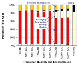
The first trend that was observed was in the makeup of the individual cost contributions (design, fabrication, testing, packaging, tooling, software development) of the total cost. Figure 4 shows a plot for the MIXED implementation using hardware foundry 1 (HW1) and software foundry 1 (SW1). At low production quantities (1000 units), design cost and tooling (wafer-masking) cost are the largest factors, dominating the total cost. As production quantity and reuse are increased, both the design and tooling percentages decrease, and fabrication cost becomes significant. This is reasonable because design and tooling costs, are nonrecurring costs, amortized over the entire production quantity. Fabrication and packaging, are recurring costs that remain constant independent of production level. Therefore, the percentage makeup of the total cost for fabrication increases steadily while design, tooling, and testing will decrease. The “Recurring” category on the plot indicates the limit as the production volume approaches infinity.
Similar trends are also observed for hardware foundry 2. Fab- rication costs are slightly higher while masking costs are lower due to the change in wafer foundry characteristics (Table 3).
More interesting results were found when the total cost figures were examined for the implementations based on the partitioning of hardware and software.
In Figure 5 a medium level of production is assumed (10,000 units). The software foundry remains a smaller factor in total cost than hardware, and combinations utilizing software foundry 2 are slightly less expensive. Software foundry 1 combinations peak between 25% and 50% custom hardware, making the minimum cost the 0% hardware or the software implementation. The software foundry 2 combinations peak similarly, and minimized cost is at 0% hardware. The software implementation does not meet performance standards so the ASIC implementation is the best choice for all foundry combinations. It is important to observe on this plot that the foundry combinations meet at 0% hardware and 100% hardware. This happens because at 100% hardware, the software foundry is irrelevant, causing the combinations HW1/SW1 and HW1/SW2 to end in the same place because only hardware costs are included. The same effect happens for hardware foundry 2. At 0% hardware, this effect is reversed, and the hardware foundry is irrelevant. Therefore,
HW1/SW1 and HW2/SW1 will meet and HW1/SW2 and HW2/SW2 will meet. When the production volume is increased there is no longer a peak in cost between 25% and 50% hardware and the optimal costs to fall at 0% hardware. Now, the MIXED implementations must be chosen due to performance constraints. It is interesting to note that although the combination of HW1/SW2 starts out less expensive than that of HW2/SW1, it becomes more expensive at approximately 5% hardware.
Hardware and software reuse was also examined at all levels of production. As the level of reuse increases, cost decreases due to design costs and software development costs decreasing. At low levels of production, reuse affects costs more because design cost and software development cost are both non-recurring and have fewer units to be amortized over. A change in those cost values has a greater affect on total cost values than at larger production rates. The effect of reuse at a medium level of production is shown in Figure 6. We can observe, for instance, that although the MIXED implementation may not be less expensive than the ASIC implementation with no reuse, if the JPEG encoder producer could increase levels of reuse to 40%, the MIXED implementation at 40% reuse could be less expensive than the ASIC implementation with no reuse. However, reuse of IP and software is effectively coupled in this approximation (which would not be the case in reality) so that 20% reuse in the ASIC
Table 3. Hardware foundries
Input HW1 HW2
Wafer diameter 8" 6"
Die-to-die spacing 0.05" 0.05"
Edge scrap 0.4" 0.4"
Wafer format No centerline cuts No centerline cuts
Technology CMOS CMOS
Min. feature size 0.18 (µm) 0.35 (µm)
Defect density 3 (defects/in2) 3 (defects/in2)
Utilization efficiency 0.5 0.5
Metal layers 6 4
Fab. wafer cost 1600 ($) 1600 ($)
Wafer probing cost 0.003 ($/IO) 0.003 ($/IO)
Probe coverage 0.75 0.75
Sawing cost 0.1 ($) 0.1 ($)
Sawing yield 0.999 0.999
Bonding format Peripheral Peripheral
Bond pad width 63.5 (µm) 63.5 (µm)
Bond pad length 76.2 (µm) 76.2 (µm)
Bond pad pitch 0.1016 mm 0.1016 mm
0% 20% 40% 60% 80% 100% 1000, No 1000, 20% 1000, 40% 10000, No 10000, 20% 10000, 40% 100000, No 100000, 20% 100000, 40% R e cu rrin g
Production Quantity and Level of Reuse
Per cen t o f T o tal Co st Software development Packaging Fabrication Tooling Design Testing 0% 20% 40% 60% 80% 100% 1000, No 1000, 20% 1000, 40% 10000, No 10000, 20% 10000, 40% 100000, No 100000, 20% 100000, 40% R e cu rrin g
Production Quantity and Level of Reuse
Per cen t o f T o tal Co st Software development Packaging Fabrication Tooling Design Testing
Figure 4. Cost breakdown for MIXED implementation using hardware foundry 1 (HW1) and software foundry 1
0 5 10 15 20 25 30 35 40 45 0 10 20 30 40 50 60 70 80 90 100
Percent Custom Hardware
Total Cost ($/chip)
HW1/SW1 HW1/SW2 HW2/SW1 HW2/SW2 0 5 10 15 20 25 30 35 40 45 0 10 20 30 40 50 60 70 80 90 100
Percent Custom Hardware
Total Cost ($/chip)
HW1/SW1 HW1/SW2
HW2/SW1 HW2/SW2
Figure 5. Total cost per chip for 10,000 units based on foundry combination.
Table 4. Software foundries
Input SW1 SW2
Assessment/assimilation 0.04 0.04
Software understanding 0.3 0.3
COTS components modified 0 0
COTS code modified 0 0
COTS integration modified 0 0
Annual change traffic 0.15 0.15
Sched. compression/expan. 1 1
All labor rates 80 ($/hr) 80 ($/hr)
Application complexity 1 1 Requirements volatility 1 0.91 Required reliability 1 0.88 Database size 1 0.94 Product complexity 1 0.85 Required reusability 1.1 1 Execution-time constraint 1.11 1 Main-storage constraint 1 1 Virtual-machine volatility 1 0.87
Computer turnaround time 1 0.87
Analyst capability 1 1.19
Application experience 0.91 1
Prog. team capability 0.86 1
Virtual-machine experience 1 1.1
Language experience 0.96 1
Modern prog. pract. (use) 0.91 1
Use of software tools 1 1.1
Classified security appl. 1.1 1
Platform 1.1 1
Req. development schedule 1.04 1
Req. maintenance reliability 1 0.98
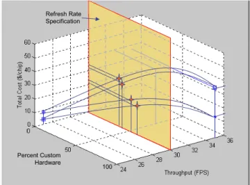
100 Percent Custom Hardware Refresh Rate Specification 100 Percent Custom Hardware Refresh Rate Specification
Figure 7. Chip cost and performance based on implementation at 10,000 units.
implementation could allow 20% reuse in the MIXED implementation; this cost improvement is assumed to be present across implementations. Therefore, reuse acts as an improvement only within each implementation. Figure 7 examines the expected cost and implementation based on trend-lines drawn through known data points. The plane drawn on the plot is set at the throughput constraint of 30 FPS. The points where the trend-lines for the different foundry combinations intersect the plan are denoted by stars, and are plotted to the corresponding percent custom hardware and cost. Because we have only considered performance ratings for the three implementations (ASIC, MIXED, and SW), we cannot draw conclusions about points in between. In many cases, at large production quantities the optimized partitioning would be between 0% and 50% hardware. Because the MIXED implementation’s refresh rate of 33 FPS (Table 1) still exceeds the refresh rate specification of 30 FPS, it may be concluded that a partition can be found that just meets the specification and is less expensive than the MIXED implementation. Figure 7 shows that while we have stated for hardware foundry 1 combinations at 10,000 units that the 100% custom hardware implementation would be optimal, an implementation exactly at the throughput constraint (if one exists)
would, in fact, be less expensive. This point falls between 0% and 50% custom hardware, hardware foundry 2 combinations remain less expensive at 100% custom hardware. Despite this demonstration, we cannot conclude as to whether points falling exactly at the 30 FPS throughput constraint could be met by a realizable implementation of hardware and software.
5.
SUMMARY AND CONCLUSIONS
In this paper, we have shown that modern hardware/software co-design methodologies can benefit from the use of comprehensive cost models early in the design process. The ability to view the effects of hardware/software partitioning choices on overall system performance and cost, may prove indispensable in future design methodologies. This paper presented a cost versus performance trade-off-based hardware/software co-design approach that enhances design space exploration early in the system development phase, allowing designers to make educated partitioning choices to meet cost and performance goals and standards. It must, however, be noted that the methodology discussed in this paper ignores the economic impact of several important system attributes, such as flexibility and upgradeability provided by software solutions.
6. REFERENCES
[1] DeBardelaben, J. Madisetti, V. and Gadient, A. J. Incorporating cost
modeling in embedded-system design. IEEE Design & Test of Computers 14, 3, (July-Sept 1997), 24-35.
[2] Boehm, B. Software Engineering Economics. Prentice-Hall, Inc., 1981.
[3] REVIC Software Cost Estimating Model User’s Manual Version 9.2. U.S. Air
Force Analysis Agency, 1994.
[4] Boehm, B., Clark, B.K., Horowitz, E., Madachy, R., Selby, R.W., and
Westland, C. Cost models for future software processes: COCOMO 2.0. Annals of Software Eng (1995).
[5] Egolf, T. W. Virtual Prototyping of Embedded Digitial Systems:
Hardware/Software Codesign, Integration, and Test. Ph.D. Dissertation, Georgia Inst. of Tech., (Dec. 1997).
[6] Gajski, D., Vahid, F., Narayan, S. and Gong, J. Specification and Design of
Embedded Systems. Prentice-Hall, Inc., NJ, 1994.
[7] Ernst, R., Henkel, J. and Benner, T. Hardware-software cosynthesis for
micorcontrollers,” IEEE Design & Test of Comp. 10, 4, (Dec 1993), 64-75.
[8] Gupta, R. and De Micheli, G. Hardware-software cosynthesis for digital
systems. IEEE Design & Test of Computers 10, 3, (Sept 1993), 29-41.
[9] Kalavade, A. and Lee, E. A Hardware-software codesign methodology for
DSP applications. IEEE Design & Test of Comp. 10, 3, (Sept 1993), 16-28. [10] Fornaciari, W., Salice, F, and Bondi, U. Development cost and size estimation
starting from high-level specifications. Proc. Int. Symposium on Hardware/Software Codesign (April 2001), 86-91.
[11] Bakshi, S. and Gajski, D. Hardware/software partitioning and pipelining. in Proceedings Design Automation Conference (June 1997), 713-716. [12] Albrecht, A. Measuring Application Development Productivity. Programming
Productivity: Issues for the Eighties. IEEE Comp Society Press. (1981). [13] Jones, T.C. Programming Productivity. McGraw-Hill, Inc., 1986. [14] Jones, T.C. Table of Programming Languages and Levels – Version 8.2.
Software Productivity Research, Burlington MA, 2001.
[15] DeBardelaben, J. An Optimization-Based Approach for Cost-Effective Embedded DSP System Design. Ph.D. Dissertation, Georgia Institute of Technology (May 1998).
[16] Donath, W. Equivalence of memory to random logic. IBM J. of Res. and Dev. 58, 5, (Sept 1974), 401-407.
[17] Sandborn, P., Abadir, M., and Murphy, C. The tradeoff between peripheral and area array bonding of components in multichip modules. IEEE Trans. CPMT, Part A 17, 2, (June 1994), 249-256.
[18] Dehkordi, P.H. and Bouldin, D.W. Design for packagability: The impact of bonding technology on the size and layout of VLSI dies. Proc. IEEE MCM Conf. (1993), 153-159.
[19] Keating, M. A Financial Model for Design Reuse. Design Reuse Group, Synopsis, Inc., 1998.
[20] Dislis, C., Dick, J.H., Dear, I.D. and Ambler, A.P. Test Economics and Design for Testability, Ellis Horwood, New York NY, 1995.
[21] Weeks, J.R. JPEG Encoder, BioElectroMech and the Independent JPEG Group, www.obrador.com /essentialjpeg/jpeg.htm, 1998.
0 5 10 15 20 25 30 35 40 Tot al Cost ( $/ chi p)
ASIC, No ASIC, 20% ASIC, 40%
MIXED, No MIXED, 20% MIXED, 40%
SW, No SW, 20% SW, 40%
Implementation and Level of Reuse HW1/SW1 HW1/SW2 HW2/SW1 HW2/SW2 HW1/SW1 HW1/SW2 HW2/SW1 HW2/SW2 0 5 10 15 20 25 30 35 40 Tot al Cost ( $/ chi p)
ASIC, No ASIC, 20% ASIC, 40%
MIXED, No MIXED, 20% MIXED, 40%
SW, No SW, 20% SW, 40%
Implementation and Level of Reuse HW1/SW1 HW1/SW2 HW2/SW1 HW2/SW2 HW1/SW1 HW1/SW2 HW2/SW1 HW2/SW2
Figure 6. Total cost per chip for 10,000 units based on foundry combinations with reuse.