System Design Considerations When Using
Cypress CMOS Circuits
This application note describes some factors to consider when either designing new systems using Cypress high-per-formance CMOS integrated circuits or when using Cypress products to replace bipolar or NMOS circuits in existing sys-tems. The two major areas of concern are device input sen-sitivity and transmission line effects due to impedance mis-matching between the source and load.
To achieve maximum performance when using Cypress CMOS ICs, pay attention to the placement of the components on the printed circuit board (PCB); the routing of the metal traces that interconnect the components; the layout and de-coupling of the power distribution system on the PCB; and perhaps most important of all, the impedance matching of some traces between the source and the loads. The latter traces must, under certain conditions, be analyzed as trans-mission lines. The most critical traces are those of clocks, write strobes on SRAMs and FIFOs, output enables, and chip enables.
Replacing Bipolar or NMOS ICs
Cypress CMOS ICs are designed to replace both bipolar ICs and NMOS products and to achieve equal or better perfor-mance at one-third (or less) the power of the components they replace.
When high-performance Cypress CMOS circuits replace ei-ther bipolar or NMOS circuits in existing sockets, be aware of conditions in the existing system that could cause the Cy-press ICs to behave in unexpected ways. These conditions fall into two general categories: device input sensitivity and sensitivity to reflected voltages.
Input Sensitivity
High-performance products, by definition, require less energy at their inputs to change state than low- or medium-perfor-mance products.
Unlike a bipolar transistor, which is a current-sensing device, a MOS transistor is a voltage-sensing device. In fact, a MOS
circuit design parameter called K′ is analogous to the gm of a
vacuum tube and is inversely proportional to the gate oxide thickness.
Thin gate oxides, which are required to achieve the desired performance, result in highly sensitive inputs. These inputs require very little energy at or above the device input-voltage
threshold (approximately 1.5V at 25°C) to be detected.
CMOS products may detect high-frequency signals to which bipolar devices may not respond.
MOS transistors also have extremely high input impedances
(5 to 10 MΩ), which make the transistors’ gate inputs
analo-gous to the input of a high-gain amplifier or an RF antenna. In contrast, because bipolar ICs have input impedances of
1000Ω or less, these devices require much more energy to
change state than do MOS ICs. In fact, a typical Cypress IC
requires less than 10 picojoules of energy to change state. Thus, when Cypress CMOS ICs replace bipolar or NMOS ICs in existing systems, the CMOS ICs might respond to pulses of energy in the system that are not detected by the bipolar or NMOS products.
Reflected Voltages
Cypress CMOS ICs have very high input impedances and—to achieve TTL compatibility and drive capacitive loads—low output impedances. The impedance mismatch due to low-impedance outputs driving high-impedance inputs might cause unwanted voltage reflections and ringing under certain conditions. This behavior could result in less-than-op-timum system operation.
When the impedance mismatch is very large, a nearly equal and opposite negative pulse reflects back from the load to the source when the line’s electrical length (PCB trace) is greater than
Eq. 1
where tr is the rise time of the signal at the source, and tpd is
the one-way propagation delay of the line per unit length. The classical way of stating the condition for a voltage reflec-tion to occur is that it will occur if the signal rise time is less than or equal to the round-trip (two-way) propagation delay of the line.
Input clamping diodes to ground were added to bipolar IC families (e.g., TTL, AS, LS, ALS, FAST) when the circuit de-signers decided that the fast rise and fall times of the outputs
could cause voltage reflections. The clamping diodes to VCC
are inherent in the junction isolation process. For a more de-tailed explanation, see “Input/Output Characteristics of Cy-press Products.”
Historically, as circuit performance improved, the output rise and fall times of the bipolar circuits decreased to the point where voltage reflections began to occur (even for short trac-es) when an impedance mismatch existed between the line and the load. Most users, however, were unaware of these reflections because they were suppressed by the diodes’ clamping action.
Conventional CMOS processing results in PN junction di-odes, which adversely affect the ESD (electrostatic dis-charge) protection circuitry at each input pin and cause an increased susceptibility to latch-up. In addition, when the in-put pin is negative enough to forward bias the inin-put clamping diodes, electrons are injected into the substrate. When a suf-ficient number of electrons are injected, the resulting current can disturb internal nodes, causing soft errors at the system level.
l tr 2tp d ---=
To eliminate the prospect of having this problem, all Cypress CMOS products use a substrate bias generator. The strate is maintained at a negative 3V potential, so the sub-strate diodes cannot be forward biased unless the voltage at the input pin becomes a diode drop more negative than –3V. (See Figure 9 in “Input/Output Characteristics of Cypress Products” for a schematic of the input protection circuit used in all Cypress CMOS products.) To the systems designer, this translates to approximately five times (3.8V divided by 0.8V =4.75) the negative undershoot safety margin for Cypress CMOS integrated circuits versus those that do not use a bias generator.
Voltage reflections should be eliminated by using impedance matching techniques and passive components that dissipate excess energy before it can cause soft errors. Crosstalk should be reduced to acceptable levels by careful PCB layout and attention to details.
Crosstalk
The rise and fall times of the waveforms generated by Cy-press CMOS circuit outputs are 2 to 4 ns between levels of 0.4 and 4V. The fast transition times and the large voltage swings could cause capacitive and inductive coupling (crosstalk) between signals if insufficient attention is paid to PCB layout.
Crosstalk is reduced by avoiding running PCB traces parallel to each other. If this is not possible, run ground traces be-tween signal traces.
In synchronous systems, the worst time for the crosstalk to occur is during the clock edge that samples the data. In most systems it is sufficient to isolate the clock, chip select, output enable, and write and read control lines from each other and from data and address lines so that the signals do not cause coupling to each other or to the data lines.
It is standard practice to use ground or power planes between signal layers on multilayered PCBs to reduce crosstalk. The capacitance of these isolation planes increases the propaga-tion delay of the signals on the signal layers, but this drawback is more than compensated for by the isolation the planes pro-vide.
The Theory of Transmission Lines
A connection (trace) on a PCB should be considered as a transmission line if the wavelength of the applied frequency is short compared to the line length. If the wavelength of the applied frequency is long compared to the length of the line, conventional circuit analysis can be used.
In practice, transmission lines on PCBs are designed to be as nearly lossless as possible. This simplifies the mathematics required for their analysis, compared to a lossy (resistive) line. Ideally, all signals between ICs travel over constant-imped-ance transmission lines that are terminated in their character-istic impedances at the load. In practice, this ideal situation is seldom achieved for a variety of reasons.
Perhaps the most basic reason is that the characteristic im-pedances of all real transmission lines are not constants, but present different impedances depending upon the frequency of the applied signal. For “classical” transmission lines driven by a single frequency signal source, the characteristic imped-ance is “more constant” than when the transmission line is driven by a square wave or a pulse.
According to Fourier series expansion, a square wave con-sists of an infinite set of discrete frequency components-the fundamental plus odd harmonics of decreasing amplitude. When the square wave propagates down a transmission line, the higher frequencies are attenuated more than the lower frequencies. Due to dispersion, the different frequencies do not travel at the same speed.
Dispersion indicates the dependence of phase velocity upon the applied frequency (see Reference 1, page 192). The re-sult is that the square wave or pulse is distorted when the frequency components are added together at the load. A second reason why practical transmission lines are not ide-al is that they frequently have multiple loads. The loads may be distributed along the line at regular or irregular intervals or lumped together, as close as practical, at the end of the line. The signal-line reflections and ringing caused by impedance mismatches, non-uniform transmission line impedances, in-ductive leads, and non-ideal resistors could compromise the dynamic system noise margins and cause inadvertent switch-ing.
One system design objective is to analyze the critical signal paths and design the interconnections such that adequate system noise margins are maintained. There will always be signal overshoot and undershoot. The objective is to accu-rately predict these effects, determine acceptable limits, and keep the undershoot and overshoot within the limits.
The Ideal Transmission Line
An equivalent circuit for a transmission line appears in Figure
1. The circuit consists of subsections of series resistance (R)
and inductance (L) and parallel capacitance (C) and shunt
admittance (G) or parallel resistance, Rp. For clarity and
con-sistency, these parameters are defined per unit length.
Multi-ply the values of R, L, C, and Rp by the length of the
subsec-tion, l, to find the total value. The line is assumed to be infinitely long.
If the line of Figure 1 is assumed to be lossless (R = 0, Rp =
infinity), Figure 1 reduces to Figure 2. A small series resis-tance has little effect upon the line’s characteristic imped-ance. In practice and by design, the series resistance is quite small. For 1-ounce (0.0015-inch-thick), 1-mil-wide (0.010-inch) copper traces on G-10 glass epoxy PCBs, the
trace resistance is between 0.5 and 0.3Ω per foot. 2-ounce
copper has a resistance 50 percent lower than that of 1-ounce copper.
Input or Characteristic Impedance
To calculate the characteristic impedance (also called AC im-pedance or surge imim-pedance) looking into terminals a-b of the circuit in Figure 2, use the following procedure.
Let Z1 be the input impedance looking into terminals a-b, with
Z2 for terminals c-d, Z3 for terminals e-f, etc. Z1 is the series
impedance of the first inductor (lL) in series with the parallel
combination of Z2 and the impedance of the capacitor (lC).
From AC theory:
Eq. 2
where XL is the inductive reactance.
Eq. 3 XL = jωlC XC 1 jωlC ---+
where XC is the capacitive reactance. Then
Eq. 4
If the line is reasonably long, Z1 = Z2 = Z3. Substituting Z1 =
Z2 into Equation 4 yields
or
Eq. 5
Substituting the expressions for XC and XL yields
Eq. 6
Equation 6 contains a complex component that is frequency
dependent. The complex component can be eliminated by allowing l to become very small and by recognizing that the
ratio L/C is constant and independent of l or ω:
Eq. 7
The AC input impedance of a purely reactive, uniform, loss-less line is a resistance. This is true for AC or DC excitation. Propagation Velocity and Delay
The propagation velocity (or phase velocity) of a sinusoid trav-eling on an ideal line (see Reference 1) is
Eq. 8 The propagation delay for a lossless line is the reciprocal of the propagation velocity:
Eq. 9 where L and C are once again the intrinsic line inductance and capacitance per unit length.
Adding additional stubs or loads to the line (see Reference 2 of this application note) increases the propagation delay by the factor
Eq. 10
where CD is the load capacitance.
Therefore, the propagation delay of a loaded line, TpdL, is
Eq. 11 Figure 1. Transmission Line Model
Figure 2. Ideal Transmission Line Model
V1 l R l L l l l R l L V2 l C l C l G TO INFINITY 1/lRp = l G V1 l L l l l L V2 l C l C TO INFINITY l Z1 Z2 Z3 Z4 l L a c e g b d f h l C V3 V4 Z1 XL Z2XC Z2+XC ---+ = Z1 XL Z1XC Z1+XC ---+ = Z12–Z1XL–XCXL = 0 Z12–jωlL L C ----= Z1 = L C⁄ α 1 LC ---= tp d = LC = Z1C 1+CD⁄C tpd L = tp d 1+CD⁄C
This application note shows later that a transmission line’s unloaded or intrinsic propagation delay is proportional to the square root of the dielectric constant of the medium surround-ing or adjacent to the line. Propagation delay is not a function of the line’s geometry.
The characteristic impedance of a capacitively loaded line de-creases by the same factor that the propagation delay in-creases:
Eq. 12
Note that the capacitance per unit length must be multiplied by the line length, l, to calculate an equivalent lumped capac-itance.
The Condition for Voltage Reflection
It is relatively straightforward to obtain a closed-form solution for a transmission line’s maximum allowable length, which, if exceeded, might cause a voltage reflection. If the line is not terminated in its characteristic impedance, a reflection is guaranteed to occur. The reflection’s amplitude depends on the amount of impedance mismatch between the line and the load and whether the rise time of the signal at the source equals or is greater (slower) than two times the propagation delay of the line.
The condition for a voltage reflection to occur is
Eq. 13 Solving for the loaded propagation delay yields
Eq. 14 However, the actual physical length of the line is
Eq. 15 The intrinsic capacitance of the line from Equation 9 is
Eq. 16
It is standard practice to use CO to designate the intrinsic line
capacitance, LO the intrinsic line self inductance, and ZO the
intrinsic line characteristic impedance.
Substituting Equations 14, 15, and 16 into Equation 11 gives the relationship for the line length at which voltage reflections might occur. Two conditions must be present for voltage re-flections to occur: the line must be long and there must be an impedance mismatch between the line and the load.
Eq. 17
Solving Equation 17 for the line length, L, yields
Eq. 18
Equation 18 is very useful to the system designer. It is generic
and applies to all products irrespective of circuit type, logic family, or voltage levels. The equation allows you to estimate when a line requires termination, using variables you can eas-ily determine.
When driving a distributed or non-lumped load, the signal’s rise time depends on the source—not the load, as you might expect. The intrinsic, or unloaded, line propagation delay per unit length is a function of the dielectric constant and can be easily calculated. The intrinsic line characteristic impedance is a function of the dielectric constant and the PCB’s physical construction or geometry and can also be calculated. Finally, you can estimate the equivalent (lumped) load capacitance by adding up the number of loads (device inputs) being driven and multiplying by 10 pF. For I/O pins, use 15 pF per pin.
Signal Transition Times
The standard Cypress 0.8µ (L drawn) CMOS process yields
output buffers whose signals transition approximately 4V in 2 ns, or, have a slew rate of 2V per nanosecond. The rise time/fall time is 2 ns. Products fabricated using the Cypress BiCMOS process have the same rise times.
The Cypress ECL process yields products with 500-ps output signal rise times and fall times, or slew rates of 1V/0.5 ns = 2V per nanosecond. Internal signal slew rates are 10V per nanosecond, but only for short (usually less than 500 mV) voltage excursions. Thus, high-frequency noise is generated on chip, which you can eliminate by using 100- to 500-pF
ceramic or mica filter capacitors between VCC and ground.
The values in Table 1 come from using Equation 18 to calcu-late the line length at which voltage reflections may occur. The
calculations assume a 50Ω intrinsic line characteristic
imped-ance and that the PCB is multilayer, using stripline construc-tion on G-10 glass epoxy material (dielectric constant of 5). These conditions result in an unloaded line propagation delay of 2.27 ns per foot. Z1' Z1 1+CD⁄C ---= L tr 2tpdL ---≥ tp dL tr 2L ---= l tr tp d ---= CO Tp d ZO ---= tr 2L --- tp d 1 CD tr tp d --- tpd ZO ---× ---+ =
Table 1. Line Length at Which a Voltage Reflection Occurs tr (ns) CD (pF) L (inches) 2 10 4.73 2 20 4.32 2 40 3.74 2 80 3.05 1 10 2.16 1 20 1.87 1 40 1.53 1 80 1.18 0.5 10 0.93 0.5 20 0.76 0.5 40 0.59 0.5 80 0.44 L tr 2 tp d --- 1 1 CDZO tr ---+ ---× =
Table 1 reveals that decreasing the source rise time from 2 to
0.5 ns (a factor of 4) decreases the line length at which a voltage reflection might occur by a factor of 5 (4.73 divided by 0.93 = 5.09) for the same load (10 pF) and intrinsic propaga-tion delay (2.27 ns/ft.). A second observapropaga-tion is that for sig-nals with rise times of 0.5 ns, all lines should be terminated.
Reflection Coefficients
Another attribute of the ideal transmission line, reflection co-efficients, are not actually line characteristics. The line is treated as a circuit component, and reflection coefficients are defined that measure the impedance mismatches between the line and its source and the line and its load. The reason for defining and presenting the reflection coefficients be-comes apparent later when it is shown that if the impedance mismatch is sufficiently large, either a negative or positive voltage might reflect back from the load to the source, and the voltage might either add to or subtract from the original signal. A mismatch between the source and line impedance may also cause a voltage reflection, which in turn reflects back to the load. Therefore, two reflection coefficients are defined. For classical transmission lines driven by a single frequency source, the impedance mismatches cause standing waves. When pulses are transmitted and the source’s output imped-ance changes depending upon whether a LOW-to-HIGH or a HIGH-to-LOW transition occurs, the analysis is complicated further.
You can use classical transmission line analysis-where puls-es are reprpuls-esented by complex variablpuls-es with exponentials-to calculate the voltages at the source and the load after several back and forth reflections. However, these complex equations tend to obscure what is physically happening.
Energy Considerations
Now consider the effects of driving the ideal transmission line with digital pulses and analyze the behavior of the line under various driving and loading conditions. The first task is to de-fine the load and source reflection coefficients.
Figure 3 shows the circuit to be analyzed. The ideal
transmis-sion line of length l is driven by a digital source of internal
resistance RS and loaded with a resistive load RL. The
char-acteristic impedance of the line appears as a pure resistance, Eq. 19 to any excitation.
The ideal case is when RS = ZO = RL. The maximum energy
transfer from source to load occurs under this condition, and no reflections occur. Half the energy is dissipated in the
source resistance, RS, and the other half is dissipated in the
load resistance, RL (the line is lossless).
If the load resistor is larger than the line’s characteristic im-pedance, extra energy is available at the load and is reflected back to the source. This is called the underdamped condition, because the load under-uses the energy available. If the load resistor is smaller than the line impedance, the load attempts to dissipate more energy than is available. Because this is not possible, a reflection occurs that signals the source to send more energy. This is called the overdamped condition. Both the underdamped and overdamped cases cause negative traveling waves, which cause standing waves if the excitation
is sinusoidal. The condition ZO = RL is called critically
damped.
The safest termination condition, from a systems design view-point, is the slightly overdamped condition, because no ener-gy is reflected back to the source.
Line Voltage for a Step Function
To determine the line voltage for a step function excitation, you apply a step function to the ideal line and analyze the behavior of the line under various loading conditions. The step function response is important because any pulse can be represented by the superposition of a positive step func-tion and a negative step funcfunc-tion, delayed in time with respect to each other. By proper superposition, you can predict the response of any line and load to any width pulse. The princi-ple of superposition applies to all linear systems.
According to theory, the rise time of the signal driven by the source is not affected by the characteristics of the line. This has been substantiated in practice by using a special coaxi-ally constructed reed relay that delivers a pulse of 18A into
50Ω with a rise time of 0.070 ns (see Reference 1).
The equation representing the voltage waveform going down the line (see Figure 3) as a function of distance and time is
for t < TO Eq. 20
Eq. 21 where
VA = the voltage at point A
X = the voltage at a point X on the line
l = the total line length
tpd = the propagation delay of the line in nanoseconds per foot
TO = l tpd, or the one-way line propagation delay
U(t) = a unit step function occurring at x = 0
VS(t) = the source voltage
When the incident voltage reaches the end of the line, a
re-flected voltage, V′, occurs if RL does not equal ZO. The
reflec-tion coefficient at the load, ρL, can be obtained by applying
Ohm’s Law.
The voltage at the load is VL + VL′, which must be equal to (IL
+ IL′)RL. But Figure 3. Ideal Transmission Line Loaded and Driven
ZO= L C⁄ ( ) l X A B ZO + + – – + – IA IB IA IB RS VS VA VB(–X) RL
SOURCE LINE LOAD
VL(X t, ) = VA( )t U t( –Xtpd) VA( )t VS( )t ZO ZO+RS --- =
Eq. 22 and
Eq. 23
(The minus sign is due to IL being negative; i.e., IL is opposite
to the current due to VL.) Therefore,
Eq. 24 By definition:
Eq. 25
Solving for VL′/VL in Equation 24 and substituting in the
equa-tion for ρL yields
Eq. 26 The reflection coefficient at the source is
Eq. 27 Re-arranging Equation 24 yields
Eq. 28
Equation 28 describes the voltage at the load (VB) as the sum
of an incident voltage (VL) and a reflected voltage (ρL Vl) at
time t = TO. When RL = ZO, no voltage is reflected. When RL
< ZO, the reflection coefficient at the load is negative; thus, the
reflected voltage subtracts from the incident voltage, giving
the load voltage. When RL > ZO, the reflection coefficient is
positive; thus, the reflected voltage adds to the incident volt-age, again giving the load voltage.
Note that the reflected voltage at the load has been defined as positive when traveling toward the source. This means that the corresponding current is negative, subtracting from the current driven by the source.
This piecewise analysis is cumbersome and can be tedious. However, it does provide an insight into what is physically happening and demonstrates that a complex problem can be solved by dividing it into a series of simpler problems. Also, eliminating the exponentials—which provide phase informa-tion in the classical transmission line equainforma-tions—simplifies the mathematics. To use the piecewise method, you must do careful bookkeeping to combine the reflections at the proper time. This is quite straightforward, because a pulse travels with a constant velocity along an ideal or low-loss line, and the time delay between reflected pulses can be predicted. The rules to keep in mind are that at any location and time the voltage or the current is the algebraic sum of the waves trav-eling in both directions. For example, two voltage waves of the same polarity and equal amplitudes, traveling in opposite
di-rections, at a given location and time add together to yield a voltage of twice the amplitude of one wave. The same reason-ing applies to all points of termination and discontinuities on the line. The total voltage or current is the algebraic sum of all the incident and reflected waves. Polarities must be observed. A positive voltage reflection results in a negative current re-flection and vice versa.
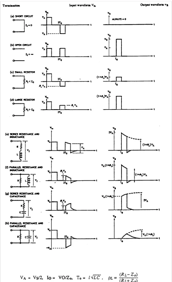
Step Function Response of the Ideal Line
Before examining reflections at the source due to mismatches between the source and line impedances, consider the be-havior of the ideal line with various loads when driven by a step function. The circuit for analysis appears in Figure 3.Figure 4 shows the voltage and current waveforms at point A
(line input) and point B (the load) for various loads. (These values are drawn from Reference 1, pg. 158–159.) Note that
RS = ZO and that VA at t = 0 equals VS/2. This means that no
impedance mismatch exists between the source and the line;
thus, there is no reflection from the source at t = 2 TO. TO is
the one-way propagation delay of the line.
The time-domain response of the reactive loads are obtained by applying a step function to the LaPlace transform of the load and then taking the inverse transform.
Note that the reflection coefficient at the load is not the total reflection coefficient (a complex number) but represents only the real part of the load. The piecewise method eliminates the
complex (jωt) terms by performing the bookkeeping involving
the phase relationships, which the complex terms account for in classical transmission line analysis.
Note that for the open-circuit condition in Figure 4b, ZL =
in-finity, so that ρL = +1. The voltage is reflected from the load to
the source (at amplitude VO = VS/2). Thus, at time t = 2 TO,
the reflected voltage adds to the original voltage, VO = VS/2,
to give a value of 2VO = VS. While the voltage wave is traveling
down to and back from the load, a current of
Eq. 29 exists. This current charges up the distributed line
capaci-tance to the value VS, then the current stops.
The waveforms at the source and load for the series RC ter-mination shown in Figure 4g are of particular interest because this network dissipates no DC power; you can use this net-work to terminate a transmission line in its characteristic im-pedance at the input to a Cypress IC. Figure 4h represents the equivalent circuit of a Cypress IC’s input. Combining both networks models a Cypress IC driven by a transmission line terminated in the line’s characteristic impedance, when the values of R and C are properly chosen.
Reflections Due to Discontinuities
Figure 5 illustrates three types of common discontinuities
found on transmission lines. Any change in the characteristic impedance of the line due to construction, connectors, loads, etc., causes a discontinuity, which causes a reflection that directs some energy back to the source. The amount of ener-gy reflected back is determined by the discontinuity’s reflec-tion coefficient. Because discontinuities are usually small by design, most of the energy is transmitted to the load. In general, a discontinuity has series inductance, shunt ca-pacitance, and series resistance. An example is a via from a
IL VL ZO ---= IL' VL' ZO ---– = VB VL+VL' VL VO --- VL' ZO ---– R L = = ρL reflected voltage incident voltage --- VL' VL ---= = ρL RL–ZO RL+ZO ---= ρS RS–ZO RS+ZO ---= VB VL+VL' 1 VL' VL ---+ V L (1+ρL)VL = = = IO VO ZO --- VS 2 ---ZO = =
signal plane through a ground plane to a second signal plane in a multilayer PCB or module. IC sockets and other connec-tors can also cause discontinuities.
The Ideal Transmission Line’s Pulse Response
Consider next the behavior of the ideal transmission line when driven by a pulse whose width is short compared to the Figure 4. Step Function Response of Figure 3 for Various Terminationsline’s electrical length-when the pulse width is less than the
line’s one-way propagation delay time, TO.
Figure 6 shows another series of response waveforms for the
circuit in Figure 3, this time for a pulse instead of a step (drawn
from Reference 1, pg. 160–161). Note that RS = ZO and that
VA at t = 0 equals VS/2. This means that there is no
imped-ance mismatch between the source and the line; thus, there
is no reflection from the source at t = 2 TO.
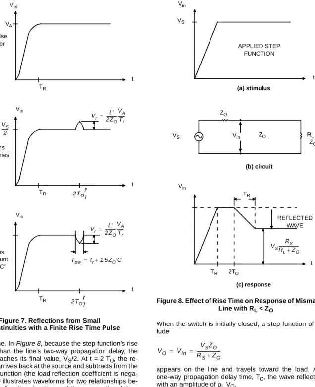
Finite Rise Time Effects
Now consider the effects of step functions with finite rise times driving the ideal transmission line. During the rise time of a pulse, half the energy in the static electric field is converted into a traveling magnetic field and half remains as a static electric field to charge the line.
If the rise time is sufficiently short, the voltage at the load changes in discrete steps. The amplitude of the steps de-pends on the impedance mismatch, and the width of the steps depends on the line’s two-way propagation delay.
As the rise time and/or the line gets shorter (smaller TO), the
result converges to the familiar RC time constant, where C is the static capacitance. All devices should be treated as trans-mission lines for transient analysis when an ideal step func-tion is applied. However, as the rise time becomes longer and/or the traces shorter, the transmission line analysis re-duces to conventional AC circuit analysis.
Reflections from Small Discontinuities
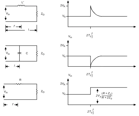
Figure 7 shows a pulse with a linear rise time and rounded
edges driving the transmission line of Figure 5a and Figure
5b. The expressions for Vr are derived on pages 171 and 172 of Reference 1. The reflection caused by the small series
in-ductance is useful for calculating the value of the inductor, L′,
but little else.
The reflection caused by the small shunt capacitor is more interesting. If this capacitor is sufficiently large, it can cause a device connected to the transmission line to see a logic 0 instead of a logic 1.
The Effect of Rise Time on Waveforms
Next, consider the ideal line terminated in a resistance less than its characteristic impedance and driven by a step func-tion with a linear rise time. The stimulus, the circuit, and the response appear in Figure 8a, Figure 8b, and Figure 8c, re-spectively. Once again, note that because the source resis-tance equals the line characteristic impedance, there are no reflections from the source.
The resulting waveforms are similar to those of Figure 4c when modified as shown in Figure 8c. The final value of the waveform must be the same as before
The resultant wave at the line input (Vin) is easily obtained by
superposition of the applied wave and the reflected wave at Figure 5. Reflections from Discontinuities with an Applied Step Function
a) Series Inductance b) Shunt Capacitance c) Series Resistance L′ Vin ZO l′ l Vin ZO Vin ZO l l′ C R Vin Vin Vin t t t 2VA 2VA 2VA VA VA VA 2VA(R+Z0) R+2Z0 ---2T0l' l --2T0l' l --2T0 l' l
the proper time. In Figure 8, because the step function’s rise time is less than the line’s two-way propagation delay, the
input wave reaches its final value, VS/2. At t = 2 TO, the
re-flected wave arrives back at the source and subtracts from the applied step function (the load reflection coefficient is nega-tive). Figure 9 illustrates waveforms for two relationships be-tween the step function rise time and the propagation delay.
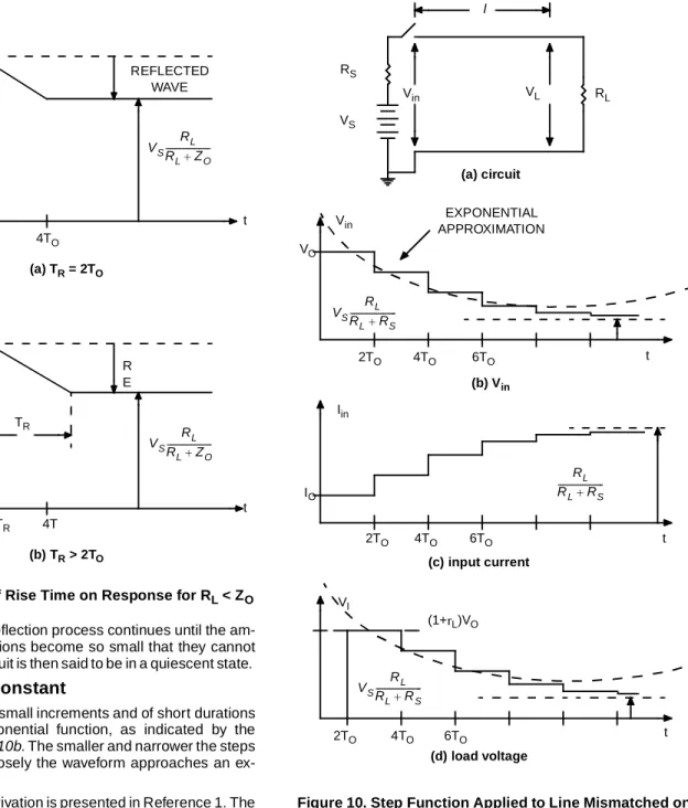
Multiple Reflections
Now consider the case of an ideal transmission line with mul-tiple reflections caused by improper terminations at both ends of the line. The circuit and waveforms appear in Figure 10. The reflection coefficients at the source and the load are both negative-the source resistance and the load resistance are both less than the line characteristic impedance.
When the switch is initially closed, a step function of ampli-tude
Eq. 30 appears on the line and travels toward the load. After a
one-way propagation delay time, TO, the wave reflects back
with an amplitude of ρL VO.
This first reflected wave then travels back to the source, and
at time t = 2 TO, the wave reaches the input end of the line. At
this time, the first reflection at the source occurs, and a wave
of amplitude ρS (ρL VO) reflects back to the load. At time t = 3
TO, this wave again reflects from the load back to the source
with amplitude
Eq. 31 Figure 7. Reflections from Small
Discontinuities with a Finite Rise Time Pulse Vin t t t Vin Vin TR TR TR
(a) Applied Pulse from Generator
(b) Reflections from Small Series
Inductor L′
(c) Reflections from Small Shunt
Capacitance C′ VA VA VS 2 ---= Vr L' 2ZO ---VA Tr ---= 2TOl' l --2TOl' l --Vr L' 2ZO ---VA Tr ---= Tpw = tr+1.5ZO'C
Figure 8. Effect of Rise Time on Response of Mismatched Line with RL < ZO APPLIED STEP FUNCTION Vin Vin Vin VS t t VS ZO ZO RL < ZO TR 2TO TR REFLECTED WAVE (a) stimulus (b) circuit (c) response VS RS RL+ZO ---VO Vin VSZO RS+ZO ---= = ρLρS(ρLVO) = ρSρL2VO
This back and forth reflection process continues until the am-plitudes of the reflections become so small that they cannot be observed. The circuit is then said to be in a quiescent state.
Effective Time Constant
Voltage reflections in small increments and of short durations approximate an exponential function, as indicated by the dashed line in Figure 10b. The smaller and narrower the steps become, the more closely the waveform approaches an ex-ponential curve.
The mathematical derivation is presented in Reference 1. The time constant is
Eq. 32 Thus, the resultant voltage waveform at the load can be ap-proximated by
Eq. 33
For Equation 32 to be accurate, ρL and ρS must be reasonably
large (approaching ±1) so that the incremental steps are
small. Because the product ρSρL is a positive number, less
than one, the time constant is a negative number, which indi-cates that the exponential decreases with time. This is usually the case in transient circuits.
Both reflection coefficients must also have the same sign to yield a continually decreasing or increasing waveform. Oppo-site signs give oscillatory behavior that cannot be represent-ed by an exponential function.
From Transmission Line to Circuit Analysis
When a transmission line is terminated in its characteristic impedance, the line behaves like a resistor. It usually does not Figure 9. Effects of Rise Time on Response for RL < ZOVin TR REFLECTED WAVE R E Vin 2TO=TR 4TO t (a) TR = 2TO (b) TR > 2TO TR 4T 2TO t VS 2 ---VS 2 ---VS RL RL+ZO ---VS RL RL+ZO ---K 2TO 1–ρSρL ---– = V t( ) VOe t K ---- =
Figure 10. Step Function Applied to Line Mismatched on Both Ends; Shown for Negative Values of ρS and ρL
EXPONENTIAL APPROXIMATION Vin 2TO t (a) circuit (b) Vin t t VO (c) input current 4TO 6TO 2TO 4TO 6TO 2TO 4TO 6TO (d) load voltage Iin IO Vl l Vin VL RS VS RL (1+rL)VO VS RL RL+RS ---RL RL+RS ---VS RL RL+RS
---matter if you use transmission line or circuit analysis, provided that you take the propagation delays into account.
Consider the case of a short-circuited transmission line driven by a step function with a source impedance unequal to the characteristic line impedance. The general case is shown in
10a. For RL = 0 the reflection coefficients are
Eq. 34 The approximate time constant is
or
Eq. 35 Recall that
Eq. 36 (one-way delay) and
Eq. 37 where l is the physical length of the line, and L and C are the per-unit-length parameters. Substituting these variables into
Equation 35 yields
Eq. 38
It is necessary to have ZS smaller than ZO. Thus, the
reflec-tion coefficients have the same sign to give exponential be-havior. Opposite signs give oscillatory bebe-havior.
If ZS < ZO, the exponential approximation becomes more
ac-curate. If ZS is very small compared to ZO, then TO is
negligi-ble compared to lL/ZO, so that Equation 35 reduces to
Eq. 39
But l L is the total loop inductance, and ZS is the circuit’s total
series impedance. The time constant is then
Eq. 40 This is the same time constant you would obtain by a circuit analysis approach if you considered the line a series
combi-nation of L′ and RS. By open-circuiting the line and performing
a similar analysis, it can be shown that an RC time constant results.
Types of Transmission Lines
The types of transmission lines include• Coaxial cable • Twisted pair • Wire over ground
• Microstrip lines • Strip lines Coaxial Cable
Coaxial cable offers many advantages for distributing high-frequency signals. The well-defined and uniform charac-teristic impedance permits easy matching. The cable’s ground shield reduces crosstalk, and the low attenuation at high frequencies make the cable ideal for transmitting the fast rise-time and fall-time signals generated by Cypress CMOS ICs. However, because of high cost, coaxial cable is usually restricted to applications that permit no alternatives. These applications usually involve clock distribution systems on PCBs or backplanes.
Because coaxial cable is not easily handled by automated assembly techniques, its application requires human assem-blers. This requirement further increases costs.
Coaxial cables have characteristic impedances of 50Ω, 75Ω,
93Ω, or 150Ω. These values are the most common, although
special cables can be made with other impedances.
Coaxial cable’s propagation delay is very low. You can com-pute it using the formula
Eq. 41
where er is the relative dielectric constant and depends upon
the dielectric material used. For solid Teflon and polyethylene, the dielectric constant is 2.3. The propagation delay is 1.54 ns per foot. For maximum propagation velocity, you can use coaxial cables with dielectric Styrofoam or polystyrene beads in air. Many of these cables have high-characteristic imped-ances and are slowed considerably when capacitively loaded. Twisted Pair
You can make twisted pairs from standard wire (AWG 24–28), twisted about 30 turns per foot. The typical characteristic
im-pedance is 110Ω.
Because the propagation delay is directly proportional to the characteristic impedance (Equation 9), the propagation delay is approximately twice that of coaxial cable. Twisted pairs are used for backplane wiring, sometimes for driving differential receivers, and for breadboarding.
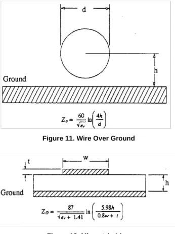
Wire Over Ground
Figure 11 shows a wire over ground. This configuration is
used for breadboarding and backplane wiring. The
character-istic impedance is approximately 120Ω. This value can vary
as much as ±40 percent, depending upon the distance from
the groundplane, the proximity of other wires, and the config-uration of the ground.
Microstrip Lines
A microstrip line (Figure 12) is a strip conductor (signal line) on a PCB separated from a ground plane by a dielectric. If the line’s thickness, width, and distance from the ground plane are controlled, the line’s characteristic impedance can be
pre-dicted with a tolerance of ±5 percent.
The formula given in Figure 12 has proven to be very accurate for width-to-height ratios between 0.1:1 and 3.0:1 and for di-electric constants between 1 and 15.
The inductance per foot for microstrip lines is
ρS ZS–ZO ZS+ZO ---,ρL –1 = = k – 2TO 1–ρSρL --- 2TO 1+ρS --- TO(ZS+ZO) ZS ---= = = k – TO TOZO ZS ---+ = TO = l LC ZO = L C⁄ k – TO lL ZS ---= = k l L ZS ---– = k L' RS ---= tpd = 1.017 er(ns/ft)
Eq. 42
where ZO is the characteristic impedance and CO is
capaci-tance per foot.
The propagation delay of a microstrip line is
Eq. 43 Note that the propagation delay depends only upon the di-electric constant and is not a function of the line width or spac-ing. For G-10 fiberglass epoxy PCBs (dielectric constant of 5), the propagation delay is 1.74 ns per foot.
Strip Lines
A strip line consists of a copper strip centered in a dielectric between two conducting planes (Figure 13). If the line’s thick-ness, width, dielectric constant, and distance between ground planes are all controlled, the tolerance of the characteristic
impedance is within ±5 percent. The equation given in is
ac-curate for W/(b – t) < 0.35 and t/b < 0.25. The inductance per foot is given by the formula
Eq. 44 The propagation delay of the line is given by the formula
Eq. 45
For G-10 fiberglass epoxy boards, the propagation delay is 2.27 ns per foot. The propagation delay is not a function of line width or spacing.
Modern PCBs
Most PCBs employ microstrip, stripline, or some combination of the two. Microstrip construction on a double-sided board with power and ground nets can suffice for low- to medi-um-performance, and low-density PCBs.
For high-performance, high-density PCBs, stripline construc-tion is preferred. Power planes isolate signal layers from each other and provide higher-quality power and grounds than those of a two-layer board. Manufacturing quality control as-sures that the metalization is of uniform thickness and that the layers are properly laminated, thus ensuring uniform, predict-able electrical characteristics.
When to Terminate Transmission Lines
Transmission lines should be terminated when they are long. From the preceding analysis, it should be apparent that
Eq. 46
where tpdL is the loaded propagation delay of the line per unit
length. For Cypress CMOS and BiCMOS products, the rise time, tr, is typically 2 ns.
For stripline construction (multilayer PCBs), the line length at which voltage reflections might occur has been shown to vary from 4.73 inches for a 10-pF load to 3.05 inches for an 80-pF load (see Equation 18 and Table 1).
Not all lines exceeding these lengths need to be terminated. Terminations are usually required on control lines (such as clock inputs, write and read strobe lines on SRAMs and FIFOs) and chip select or output-enable lines on RAMs, PROMs, and PLDs. Address lines and data lines on RAMs and PROMS usually have time to settle because they are normally not the highest-frequency lines in a system. Howev-er, if very heavily loaded, address and databus lines might require terminations.
Line Termination Strategies
There are two general strategies for transmission line termi-nation:
1. Match the load impedance to the line impedance 2. Match the source impedance to the line impedance Figure 11. Wire Over Ground
Figure 12. Microstrip Line
L = (ZO)2CO
tp d = 1.017 0.45er+0.67(ns/ft)
L = (ZO)2CO
tpd = 1.017 er(ns/ft)
Figure 13. Strip Line Construction
Long Line tr 2tp dL --->
In other words, if either the load reflection coefficient or the source reflection coefficient can be made to equal zero, re-flections are eliminated. From a systems design viewpoint, strategy 1 is preferred. Eliminating the reflection at the load (i.e., dissipating the excess energy) before the energy travels back to the source causes less noise, electromagnetic inter-ference (EMI), and radio frequency interinter-ference (RFI).
Multiple Loads, Buses, and Nodes
In the case where multiple loads are connected to a transmis-sion line, only one termination circuit is required. The termi-nation should be located at the load that is electrically the greatest distance from the source. This is usually the load that is the greatest physical distance from the source. A point-to-point or daisy chain connection of loads is preferred. Bidirectional buses should be terminated at each end with a circuit whose impedance equals the intrinsic, characteristic line impedance. The reason is that each transmitting device sees the characteristic impedance of the line when the device is transmitting.
Consider next a line that has three bidirectional nodes: one on each end and one in the middle. The middle node, when
driving the line, sees an impedance equal to ZO/2, because
the node is looking into two lines in parallel with each other.
The end nodes, however, see an impedance of ZO. In this
case, as in a backplane, each end of the line should be
termi-nated in an impedance equal to ZO/2. When heavily loaded,
Equation 12 must be used to calculate the loaded
character-istic impedance, and this must be used instead of ZO.
Types of Terminations
There are three basic types of terminations: series damping, pull-up/pull-down, and parallel AC terminations. Each has its advantages and disadvantages.
Except for series damping, the termination network should be attached to the input (load) that is electrically the greatest distance from the source. Component leads should be as short as possible to prevent reflections due to lead induc-tance.
Series Damping
Series damping is accomplished by inserting a small resistor
(typically 10Ω to 75Ω) in series with the transmission line, as
close to the source as possible (Figure 14). Series damping is a special case of damping in which the series resistor value plus the circuit output impedance equals the transmission line impedance. The strategy is to prevent the wave reflected back from the load from reflecting back from the source. This is done by making the source reflection coefficient equal to zero.
The channel resistance (on resistance) of the pull-down
de-vice for Cypress ICs is 10Ω to 20Ω, depending upon the
cur-rent-sinking requirements. Thus, subtract this value from the
series-damping resistor, Rd.
Eq. 47 A disadvantage of the series-damping technique, as illustrat-ed in Figure 15, is that during the two-way propagation delay time of the signal edges, the voltage at the input to the line is halfway between the logic levels, due to the voltage divider
action of RS. The “half voltage” propagates down the line to
the load and then back from the load to the source. This means that no inputs can be attached along the line, because they would respond incorrectly during this time. However, you can attach any number of devices to the load end of the line because all the reflections are absorbed at the source. If two or more transmission lines must be driven in parallel, the val-ue of the series-damping resistor does not change.
The advantages of series termination are: • Requires only one resistor per line
• Consumes little power
• Permits incident wave switching at the load after a TO
prop-agation delay
Figure 14. Series Damping Termination
A B C
ZO
TO
Rd
ZO = RS+Rd
• Provides current limiting when driving highly capacitive loads; the current limiting also helps reduce groundbounce The disadvantages of series termination are:
• Degrades rise time at the load due to increased RC time constant
• Should not be used with distributed loads
The low input current required by Cypress CMOS ICs results in essentially no DC power dissipation. The only AC power required is to charge and discharge the parasitic capacitanc-es.
Pull-Up/Pull-Down Termination
The pull-up/pull-down resistor termination shown in Figure 16 is included for historical reasons and for the sake of complete-ness. For TTL driving long cables, such as ribbon cables, the
values R1 = 220Ω and R2 = 330Ω are recommended by
sev-eral bus interface standards. If the cable is disconnected, the voltage at point B is 3V, which is well above the 2V minimum high TTL specification. Because most control signals are ac-tive LOW, a disconnected cable results in the unasserted state.
The maximum value of R1 is determined by the maximum
acceptable signal rise time, which is a function of the charging
RC time constant. The minimum value of R1 is determined by
the amount of current the driver can sink. The value of R2 is
chosen such that a logic HIGH is maintained when the cable is disconnected. The equivalent Thévenin resistance is
Eq. 48
The value of R1 and R2 in parallel is slightly less than the
cable’s characteristic impedance. Ribbon cables with
charac-teristic impedances of 150Ω are typical.
If both resistors are used, DC power is dissipated all the time.
If only a pull-down resistor (R2) is used, DC power is
dissipat-ed when the input is in the logic HIGH state. Conversely, if
only a pull-up resistor (R1) is used, power is dissipated when
the input is in the LOW state. Due to these power dissipations, this termination is not recommended.
If an unterminated control signal on a PCB is suspected of causing a problem, a resistor whose value is slightly less than
the characteristic impedance of the line (e.g., 47Ω) can be
connected between the input pin and ground. Be sure that the driver can source sufficient current to develop a TTL high volt-age level (2.0V) across the resistor.
In special cases where inputs should be either pulled up (HIGH) for logic reasons or because of very slow rise and fall
times, you can use a pull-up resistor to VCC in conjunction
with the terminating network shown in Figure 17. DC power is dissipated when the source is LOW.
Parallel AC Termination
Figure 17 illustrates the recommended general-purpose
ter-mination. It does not have the disadvantage of the half-volt-age levels of series damping terminations, and it causes no DC power dissipation. You can attach loads anywhere along the line, and they see a full voltage swing.
The disadvantage is that a parallel AC termination requires two components, versus the one-component series-damping termination.
Commercially Available RC Networks
A variety of combinations of R and C values are available as series RC networks in SIP packages from at least two sourc-es.
Bourns calls these networks the Series 701 and 702 RC Ter-mination Networks. You can obtain datasheets by calling the factory in Logan, Utah (801-750-7200) or a local sales office. Thin Film Technology also refers to the networks as RC Ter-mination Networks. You can obtain datasheets by calling the factory in North Mankato, Minnesota at 507-635-8445. Dale Electronics calls their product Resistor/Capacitor Net-works. Call 915-595-8139 for information.
California Micro Devices calls their product R–C Networks. Call 408-263-3214 for information.
Low-Pass Filter Analysis
The parallel AC termination has another advantage: it acts as a low-pass filter for short pulses. You can verify this by ana-lyzing the response of the circuit illustrated in Figure 18 to a positive and a negative step function. The positive step func-tion is generated by moving the switch from posifunc-tion 2 to po-sition 1. The negative step function is generated by moving the switch from position 1 to position 2. The response of the circuit to a pulse is the superposition of the two separate re-sponses. The input impedance of the Cypress circuits con-nected to the termination network are so large that they can be ignored for this analysis.
Classic circuit analysis usually assumes an ideal source (R1
= R2 = 0). In real-world digital circuits, the source output
im-pedance is not only non-zero, but also varies depending upon whether the output is changing from LOW to HIGH or vice versa. Figure 16. Pull-Up/Pull-Down R1 A B ZO R2 VCC RT R1R2 R1+R2 ---=
Figure 17. Parallel AC Termination
A B
ZO
R < ZO C
For Cypress ICs, 100Ω > R1 > 50Ω and 20Ω > R2 > 10Ω, depending upon speed and output current-sinking require-ments.
Positive Step Function Response
The initial voltage on the capacitor is zero. At t = 0, the switch is moved from position 2 to position 1. At t = 0+, the capacitor appears as a short circuit, and the voltage V is applied
through R1 to charge the load (R3C). The voltage across the
capacitor VC(t), is
Eq. 49 In theory, the voltage across the capacitor reaches V when t equals infinity. In practice, the voltage reaches 98 percent of V after 3.9 RC time constants. You can verify this by setting
VC(t)/V = 0.98 in Equation 49 and solving for t.
Negative Step Function Response
The capacitor is charged to approximately V. At t = 0, the switch is moved from position 1 to position 2, and the
capac-itor is discharged. The voltage across the capaccapac-itor, VC(t) is
Eq. 50 The voltage decays to 2 percent of its original value in 3.9 RC
time constants. You can verify this by setting VC(t)/V =0.02 in
Equation 50 and solving for t.
The Ideal Case
Consider the ideal case where R1 = R2 = 0. Let R3 = R in
Equations 49 and 50. If a positive pulse of width T is applied
to the modified circuit of Figure 18, the pulse disappears if 4RC > T.
Because the discharging time constant is the same as the charging time constant for the ideal case, a negative-going pulse of width T also disappears if 4RC > T. That is, if the applied signal is normally HIGH and goes LOW, as does the write strobe on an SRAM, the termination filters out all nega-tive glitches less than 4 RC time constants in width.
The maximum frequency that the circuit passes is
Eq. 51 This is true because the charging and discharging time con-stants are equal for the ideal case.
Capacitance for the Ideal Case
The value of the capacitor, C, must be chosen to satisfy two conflicting requirements. First, the capacitor should be large enough to either absorb or supply the energy contained or removed when positive-going or negative-going glitches oc-cur. Second, the capacitor should be small enough to avoid either delaying the signal beyond some design limit or slowing the signal rise and fall times to more than 5 ns.
A third consideration is the impedance caused by the
capac-itor’s capacitive reactance, XC. The digital waveforms applied
to the AC termination can be expressed as a Fourier Series so that they can be manipulated mathematically. However, because these signals are not periodic in the classical
mean-ing of the word, it is not clear that the AC steady-state analysis
model of XC applies here.
In most applications, the degradation of the signal’s rise and fall times beyond 5 ns determines the maximum value of the capacitor. The procedure is to calculate the rise time between the 10- and 90-percent amplitude levels, equate this rise time to 5 ns, and solve for C in terms of R:
Eq. 52 for t yields
Eq. 53
For
For
The time for the signal to transition from 10 to 90 percent of its final value is then T = 2.2 RC. Solving for C yields
Eq. 54 For T = 5 ns, Table 2 can be constructed. This table indicates
that 50Ω transmission lines on PCBs that are terminated with
RC networks should use a 47Ω resistor and a capacitor of 48
pF max; 47 pF is a standard value. This network eliminates glitches of 9 ns or less. The table’s second column applies to wirewrapping construction, which is not recommended for systems operating at frequencies over 10 MHz. An exception is if the system consists of less than six MSI or SSI ICs.
. VC( )t V 1 e t – R1+R3 ( )C ---– = VC( )t Ve t – R2+R3 ( )C ---= F max( ) 1 2T ---=
Figure 18. Lumped Load; AC Termination
Table 2. Termination Value for an Ideal Case
PCB Wirewrapped ZO (Ω) 50 120 R (Ω) 47 110 V 1 R1 2 R2 SOURCE LOAD V(t) C R3 V t( ) V 1 e t – R C ---– = t RC 1 1 V t( ) V ---– ---ln = V t( ) V --- = 0.1 t, = 0.10 RC. V t( ) V --- = 0.9 t, = 2.3 RC. C T 2.2R ---=
The Real World
To go from the ideal to the real world, calculate the values of
R1 and R2 from the curves on the datasheet of the device
driving the line. R1 is the slope of the output source current
vs. output voltage between 2 and 4V. R2 is the slope of the
output sink current vs. output voltage between 0 and 0.8V.
Add the value of R1 to 47Ω and calculate C, using Equation
54. Then check to see that the RC charging time constant
does not violate some minimum positive pulse-width specifi-cation for the line. If so, reduce C.
Add the value of R2 to 47Ω and calculate C. Then check to
see if the discharging RC time constant violates some mini-mum pulse-width specification for the line. If so, reduce C. If the line is heavily loaded, Equation 12 must be used to calculate the loaded characteristic impedance, which deter-mines the maximum value of R. The Maximum value of C is then calculated using Equation 54.
Schottky Diode Termination
In some cases it can be expedient to use Schottky diodes or fast-switching silicon diodes to terminate lines. The diode switching time must be at least four times as fast as the signal rise time. Where line impedances are not well defined, as in breadboards and backplanes, the use of diode terminations is convenient and can save time.
A typical diode termination appears in Figure 19. The
Schot-tky diode’s low forward voltage, Vf (typically 0.3 to 0.45V),
clamps the input signal to a Vf below ground (lower diode) and
VCC + Vf (upper diode). This significantly reduces signal
un-dershoot and overshoot. Some applications may not require both diodes.
The advantages of diode terminations are: • Impedance matched lines are not required
• The diodes replace terminating resistors or RC termina-tions
• The diodes’ clamping action reduces overshoot and under-shoot
• Although diodes cost more than resistors, the total cost of layout might be less because a precise, controlled trans-mission-line environment is not required
• If ringing is discovered to be a problem during system de-bug, the diodes can be easily added
As with resistor or RC terminations, the leads should be as short as possible to avoid ringing due to lead inductance. A few of the types of Schottky diodes commercially available are
• HSMS-2822 (Hewlett-Packard) • 1N5711
• MBD101, MBD102 (Motorola)
• SN74S1050/52/56 (TI, single-diode arrays) • SN74S1051/53 (TI, double-diode arrays)
Unterminated Line Example
The following example illustrates the procedure for calculating the waveforms when a Cypress PLD generates the write strobe for four Cypress FIFOs. The PLD is a PALC16L8 de-vice and the FIFOs are CY7C429s.
The equivalent circuit appears in Figure 20 and the unmodi-fied driving waveform in Figure 21. The rise and fall times are 2 ns. The length of the stripline trace on the PCB is 8 inches
and the intrinsic characteristic line impedance is 50Ω. The
voltage waveforms at the source (point A) and the load (point B) must be calculated as functions of time. Stripline construc-tion is used for this example because in most modern high-performance digital systems, the PCBs have multiple layers.
The equivalent ON channel resistance of the PLD pull-up
de-vice, 62Ω, is calculated using the output source current
ver-sus voltage graph, over the region of interest (2 to 4V), from the PALC20 series datasheet. The equivalent resistance of
the pull-down device, 11Ω, is calculated in a similar manner,
using the output sink current versus output voltage graph, over the region of interest (0.4 to 2V), also on the datasheet.
C (max., pF) 48 20
RC (ns) 2.25 2.2
4RC (ns) 9 8.8
Figure 19. Schottky Diode Termination Table 2. Termination Value for an Ideal Case
VCC
Figure 20. Equivalent Circuit for Cypress PAL Driving
VCC = 5V + 1V – 62Ω 1 2 11Ω l l = 8″ A B + – VA + – 40 pF 1.25 MΩ VB
The equivalent input circuit for the FIFO is constructed by approximating the input and stray capacitance with a 10-pF
capacitor and the input resistance with a 5-MΩ resistor. The
input leakage current for all Cypress products is specified as
a maximum of ±10 µA, which guarantees a minimum of 500
KΩ at Vin = 5V. Typical leakage current is 10 pA.
Because the PLD is driving four FIFOs in parallel, the alent lumped capacitance is 4 x 10 pF = 40 pF, and the
equiv-alent lumped resistance is 5,000,000/4 = 1.25 MΩ.
The next step is to calculate the propagation delay and the loaded characteristic impedance of the line. The unloaded propagation delay of the line is calculated using Equation 45 with a dielectric constant of 5:
Eq. 55 To calculate the loaded line propagation delay, the intrinsic capacitance must first be calculated using Equation 9.
Eq. 56
where ZO is the intrinsic characteristic impedance, and CO is
the intrinsic capacitance.
Eq. 57 Because the line is loaded with 40 pF, Equation 11 is used to compute the loaded propagation delay of the line.
Eq. 58 Note that the capacitance per unit length must be multiplied by the line length to arrive at an equivalent lumped capaci-tance.
The intrinsic line impedance is reduced by the same factor by which the propagation delay is increased (1.524; see
Equa-tion 12):
Eq. 59
Initial Conditions
At time t = 0, the circuit shown in Figure 20 is in a quiescent state. The voltage at points A and B must be the same. By inspection:
Eq. 60
At t = 0, the driving waveform changes from 4V to approxi-mately 0V with a fall time of 2 ns. This is shown in Figure 20 by the switch arm moving from position 1 to position 2. The wave propagates to the load at the rate of 3.46 ns per foot and arrives there
Eq. 61 later, as illustrated in Figure 22b.
Because the reflection coefficient at the load is ρL = 1, an
early equal and opposite polarity waveform is propagated back to the source from the load. The reflection arrives at t
=2TO = 4.6 ns (Figure 22a). Note that the fall time is
pre-served.
The reflection coefficient at the source is
Eq. 62 To simplify the calculations that follow, consider –0.5 to be the low-level source reflection coefficient. The magnitude of the reflected voltage at the source is then
Eq. 63 This wave propagates from the source to the load and arrives
at t = 3 TO. The wave adds to the 0V signal. The rise time is
preserved, and thus the time required for the signal to go from 0 to 2V is
Eq. 64 The signal at the load thus reaches the 2V level at time
Eq. 65 and remains at that level until the next reflection occurs at
Eq. 66
The wave that arrives at the load at 3 TO reflects back to the
source and arrives at Figure 21. VA(t), Unmodified 1V 0 VA(t) 24 20 0 2 22 24 t tpd = 2.27 ns/ft( ) tpd = ZOCO CO tp d ZO --- 2.27 ns/ft 50 --- 45.4 pF/ft. = = = tpd L = tp d 1+CD⁄CO tpd L 2.27 ns/ft 1 40 pF 45.4 pF/ft 8 in 12 in/ft ---× ---+ = tpd L = 3.46 ns/ft ZO' 50Ω 1.524 --- 32.8Ω = = VA VB (VC C–Vf) RL RS+RL --- = = 5–1 ( ) 1.25×10⁶ 28+1.25×10⁶ --- = = 4V TO 3.46 ns/ft 8 in. 12 in./ft ---× 2.3 ns = = ρS RS–ZO' RS+ZO' --- 11–32.8 11+32.8 --- –0.498 = = = VS1 = –4V×(–0.5) = 2V tr 2V×2 ns 4V --- 1 ns = = t = 3TO+1 ns = 7.9 ns t = 5TO
Figure 22a. Unterminated Line Example; VA(t)
Figure 22b. Unterminated Line Example; VB(t)
VA 4 3 2 1 0 –1 –2 –3 –4 0 2 4 6 8 10 12 14 18 20 22 24 0 2 4 6 8 t 16 2TO 4TO 6TO 8TO 10TO 2TO 4.6 6.6 9.2 10.2 13.8 18.4 23 4.6 6.58 8.58 2.284 VB 4 3 2 1 0 –1 –2 –3 –4 0 2 4 6 8 10 12 14 18 20 22 24 0 2 4 6 8 t 4.3 2.85 3.84 4.47 4 TO 3TO 5TO 7TO 9TO TO 3TO 2.3 4.3 6.9 7.9 11.5 16 20.7 2.3 6.9