Automated Synthesis and Optimization of
Multilevel Logic Circuits
by
Lingli Wang
©
Copyright by Lingli Wang 2000A thesis presented in partial fulfilment of the requirements for the degree of
Doctor of Philosophy
Napier University
School of Engineering
Declaration
I declare that no portion of the work referred to in this thesis has been submitted in support of an application of another degree, qualification or other academic awards of this or any other university or institution of learning.
Acknow ledgements
I am deeply indebted to my research supervisor, Professor A. E. A. Almaini, School of Engineering, Napier University, for his constant guidance, encouragement, friendship, and interest to all that I did during this research. I am grateful to Professor Almaini for taking his precious time to provide regular comments and invaluable suggestions. Many ideas of this thesis were produced during our weekly meetings. He also taught me patiently the proper style of scientific writing in English and corrected my research papers and this thesis.
I would like to thank Mr Alex Bystrov, a former member of the digital techniques group, for his essential support to help me learn Linux operating system and GNU C language programming environment when I started this research.
Thanks are due to other members of the digital techniques group, especially Mr Yinshui Xia and Mr Belgasem Ali, for their enjoyable working environment and various discussions.
I would like to thank our technician, Mr Jay Hoy for his kindly support to install Linux operating system.
This project was funded by the School of Engineering (formerly the Department of Electrical, Electronic and Computing Engineering), Napier University, Edinburgh. This support is gratefully acknowledged.
Finally, I would like to thank my wife, Xiaowen Zhong, for her everlasting love, under-standing and patience throughout my research work.
Contents
List of Abbreviations List of Figures List of Tables Abstract 1 Introduction1.1 A historic perspective of logic design . . . . 1.2 VLSI chip design methodology based on logic synthesis . 1.3 Two-Level versus multilevel logic synthesis . . . 1.4 Reed-Muller logic based on AND /XOR operations 1.5 Structure of this thesis . . . .
2 Conventional Multilevel Logic Synthesis 2.1 Algorithmic approach
2.2 Rule-Based approach 2.3 BDD approach . . . 2.4 FPGA approach
2.5 Several other approaches based on perturbation
3 Multilevel Logic Minimization Using Functional Don't Cares 3.1 Introduction . . . .
3.2 Multilevel Karnaugh map technique
3.3 Multilevel logic synthesis for large Boolean functions 3.4 Experimental results
3.5 Summary . . . . . .
4 Multilevel Minimization for Multiple Output Logic Functions 4.1 Introduction...
4.2 Review of Functional Don't Cares. 4.3 Simplification for single output functions
4.4 Multilevel minimization for multiple output functions.
vi IX Xl xii 1 1
4
7 8 10 12 12 15 16 18 20 22 22 23 29 38 40 41 41 4144
464.5 Experimental results 4.6 Summary . . . .
5 Polarity Conversion for Single Output Boolean Functions 5.1 Introduction . . . .
5.2 Basic definitions and terminology
5.3 Conversion of the coefficients with zero polarity 5.4 Conversion of the coefficients with a fixed polarity 5.5 Conversion algorithm for large Boolean functions 5.6 Algorithm and experimental results.
5.7 Summary . . . . 49 50 51 51 51 53 56 61 65 70
6 Conversion Algorithm for Very Large Multiple Output Functions 71
6.1 Introduction. 71
6.2 Algorithm.. 74
6.3 Experimental Results. 76
6.4 Summary . . . .
7 Exact Minimization of Fixed Polarity Reed-Muller Expressions 7.1 Introduction.
7.2 Background .
7.3 Properties of the polarities for SOP and FPRM expressions 7.4 Best polarity for single output functions ..
7.5 Best polarity for multiple output functions. 7.6 Experimental results
7.7 Summary . . . .
8 Optimization of Reed-Muller PLA Implementations 8.1 Introduction . . . .
8.2 Review of the decomposition method
8.3 Improved decomposition method for large single output functions 8.4 Generalization to multiple output functions
8.5 Experimental results 8.6 Summary . . . .
9 Conclusions and Future Work Publications
References and Bibliography Disk Containing the Software
77 78 78 79 83 93 95 98 99 101 101 103 106 116 122 123 125 128 129 141
List of Abbreviations
ASIC ATPG BDD BDP BLIF CAD CLB CNF CMOS CPU DAG DC DD DNF EDA EDIF ESOPApplication Specific Integrated Circuit Automatic Test Pattern Generation Binary Decision Diagram
Binary Decision Program
Berkeley Logic Interchange Format Computer Aided Design
Configurable Logic Block Conjunction Normal Form
Complementary Metal-Oxide-Semiconductor Central Process Unit
Directed Acyclic Graph Don't Care
Decision Diagram Disjoint Normal Form
Electronic Design Automation
Electronic Design Interchange Format Exclusive Sum-Of-Products
EXOR(XOR) EXclusive OR operation FDD
FPGA FPLA FPRM GA
Functional Decision Diagram Field Programmable Gate Array Field Programmable Logic Array Fixed Polarity Reed-Muller Genetic Algorithm
List of Abbreviations
GCC GNU Compiler Collection
GDB GNU DeBugger
HDL Hardware Description Language IC Integrated Circuit
IWLS International Workshop on Logic Synthesis KISS Keep Internal State Simple
LSB Least Significant Bit
LUT Look-Up Table
MCNC Microelectronics Center North Carolina
MIS Multilevel logic optimization system developed at Berkeley MPGA Mask Programmable Gate Array
MSB Most Significant Bit
MUX Multiplexer
NP Nondeterministic Polynomial, Non-Polynomial NRE N on-Recurring Engineering
OBDD Ordered Boolean Decision Diagram ODC Observability Don't Care
OFDD Ordered Functional Decision Diagram OVAG Output Value Array Graph
P &R Placement & Routing PLA Programmable Logic Array PLD Programmable Logic Device PROM Programmable Read-Only Memory PPRM Positive Polarity Reed-Muller
RMPLA Reed-Muller Programmable Logic Array ROBDD Reduced Ordered Binary Decision Diagram
RTL SCRL SDC SIS SLIF SOC SOP SRAM VHDL VLSI XNF List of Abbreviations
Register and Transfer Level Split-level Charge Recovery Logic Satisfiability Don't Care
Sequential Interactive System Stanford Logic Interchange Format System-On-Chip
Sum-Of-Products
Static Random Access Memory
Very large scale Hardware Description Language Very Large Scale Integration
List of Figures
Classical symbols for contacts 1.1
1.2 Moore's law the growth of Intel microprocessors 1.3 Historic perspective of logic design
1.4 A VLSI design model. . . . 1.5 An ASIC chip design flow . . .
1.6 Comparison between two-level and multilevel structures 1. 7 Structure of this thesis . . . . 2.1 DAG representation of a combinational Boolean network 2.2 A circuit pattern and its replacement . . . . 2.3 BDD representation of the Boolean function in example 2.1 2.4 Logic circuit from fig.2.3(b) . . . .
2.5 Typical FPGA architecture . . . . 2.6 Different partitions for the same Boolean network
3.1 Comparison between two-level and multilevel K-map methods 3.2 Multilevel K-map method for an incompletely specified function. 3.3 Two examples for definition 3.3
3.4 Examples of theorem 3.3 . . . 3.5 An example of procedure 3.2 4.1 Explanation of the functional DCs 4.2 Example of functional DCs
4.3 Results of ryy6 with 16 inputs. 4.4 Simplification of Boolean relation
5.1 Bidirectional conversion between SOP and FPRM forms 5.2 Conversion algorithm using multiple segment technique. 5.3 Bidirectional conversion algorithm for large Boolean functions 5.4 CPU Time versus the number of on-set coefficients for conversion 5.5 CPU time for parity function conversions
2 3 4 5 6 8 11 13 15 17 18 19 20 26 29 30 33 38 43 44 46 48 60 65
67
69 70List of Figures
6.1 Functional decision diagrams for
f
= X2 EB XIXO EB X3X2XIXO 6.2 An example for algorithm 6.1 . . . . 7.1 Example for a 3-variable 2-output Reed-Muller function 8.1 Limitation of i-majority m-cubes8.2 Structures of Reed-Muller PLAs 8.3 Example of procedure 8.1
8.4 Order of ~-majority cubes . . . . 8.5 Example of procedure 8.2
8.6 Boolean function of example 8.4 8.7 Example for procedure 8.3 8.8 Example for procedure 8.4
73 75 98 104 104 108 110 112 113 115 117
List of Tables
1.1 Some commercial design synthesis tools 5
2.1 Brief comparison of FPGA programming techniques 19
3.1 Comparison for single output functions run on the same PC . . . . . 39 4.1 4.2 5.1 5.2 5.3 5.4 6.1 6.2 7.1 7.2 8.1 8.2
Literal numbers with different encodings for table5
Results for multiple output functions . Truth table of the criterion function gj
Example of multiple segment technique
Conversion results of some random coefficient sets . Test results for conversion of parity functions
Distribution of dependent variables . . . . Experimental results of very large functions from IWLS'93 benchmark Test results for small Boolean functions
Test results for large Boolean functions .
Comparison with ESPRESSO for general multiple output functions . Comparison with ESPRESSO for very large multiple output functions
49 49 55 64 68 69 74 76 100 100 123 123
Abstract
With the increased complexity of Very Large Scaled Integrated (VLSI) circuits, multi-level logic synthesis plays an even more important role due to its flexibility and compact-ness. The history of symbolic logic and some typical techniques for multilevel logic synthesis are reviewed. These methods include algorithmic approach; Rule-Based approach; Binary Decision Diagram (BDD) approach; Field Programmable Gate Array(FPGA) approach and several perturbation applications.
One new kind of don't cares (DCs), called functional DCs has been proposed for multi-level logic synthesis. The conventional two-multi-level cubes are generalized to multimulti-level cubes. Then functional DCs are generated based on the properties of containment. The con-cept of containment is more general than unateness which leads to the generation of new DCs. A separate C program has been developed to utilize the functional DCs generated as a Boolean function is decomposed for both single output and multiple output functions. The program can produce better results than script.rugged of SIS, developed by UC Berke-ley, both in area and speed in less CPU time for a number of testcases from MCNC and IWLS'93 benchmarks.
In certain applications, ANDjXOR (Reed-Muller) logic has shown some attractive ad-vantages over the standard Boolean logic based on AND JOR operations. A bidirectional conversion algorithm between these two paradigms is presented based on the concept of po-larity for sum-of-products (SOP) Boolean functions, multiple segment and multiple pointer facilities. Experimental results show that the algorithm is much faster than the previously published programs for any fixed polarity. Based on this algorithm, a new technique called redundancy-removal is applied to generalize the idea to very large multiple output Boolean functions. Results for benchmarks with up to 199 inputs and 99 outputs are presented.
Applying the preceding conversion program, any Boolean functions can be expressed by fixed polarity Reed-Muller forms. There are 2n polarities for an n-variable function and the number of product terms depends on these polarities. The problem of exact polarity minimization is computationally extensive and current programs are only suitable when
n :::; 15. Based on the comparison of the concepts of polarity in the standard Boolean logic
and Reed-Muller logic, a fast algorithm is developed and implemented in C language which can find the best polarity for multiple output functions. Benchmark examples of up to 25 inputs and 29 outputs run on a personal computer are given.
After the best polarity for a Boolean function is calculated, this function can be further simplified using mixed polarity methods by combining the adjacent product terms. Hence, an efficient program is developed based on decomposition strategy to implement mixed polarity minimization for both single output and very large multiple output Boolean func-tions. Experimental results show that the numbers of product terms are much less than the results produced by ESPRESSO for some categories of functions.
Chapter
1
Introduction
1.1
A
historic perspective of logic design
In 1854, when George Boole published his principle work, An Investigation of the Laws of Thought on Which Are Founded the Mathematical Theories of Logic and Probabilities, a new branch of mathematics, Symbolic Logic, was established[22]. Logic propositions and operations started to be represented by symbols although it had already been expressed by natural language in times of Aristotle, the fourth century B.C. Ever since, great progress has been made in the field of Symbolic Logic by the broad application of algebraic meth-ods and facilities[36, 79, 95]. Until 1938, Symbolic Logic was used only as another tool of philosophy and mathematics. In that year, a graduate student at Massachusetts In-stitute of Technology recognized the connection between electronic switching circuits and Symbolic Logic and published a classic paper, entitled" A Symbolic Analysis of Relay and Switching Circuits" [135]. Based on that paper, both logic values, "TRUE" and "FALSE" can be mapped into "MAKE" and "BREAK" states of a two-state device so that logic ma-nipulations can be realized by switching circuits. Since then, many switching circuits and systems for communication, automatic control, and data processing have been designed by applying Symbolic Logic, which later came to be known as Boolean Algebra[63, 77, 84, 96, 99, 117].
During the early days, logic functions usually expressed by truth tables, Karnaugh maps[84], and algebraic formulas, either DNFs( disjoint normal forms) or CNFs( conjunction normal forms).l Besides, a two-state switch or contact is usually realized by relay, magnetic core, rectifying diode, electron tube, or cryotron operated with the aid of electromagnet[77]. The physical nature of the two stable states may take such forms as conducting versus non-conducting; closed versus open; charged versus discharged; positively magnetized versus negatively magnetized; high potential versus low potential etc. The two states of a switch were generally called "break" and "make" contacts whose common symbols are shown in
Chapter 1. Introduction
o--o----.r
I1 - 0
1]
o~---;x~--<o
(a) symbols for break contacts
O~--+----<O
(b) symbols for make contacts
Figure 1.1: Classical symbols for contacts
Section 1.1
fig. 1. 1. This research, that can be found mainly in [63, 77, 99], becomes the classical method of logic minimization for both combinational and sequential systems.
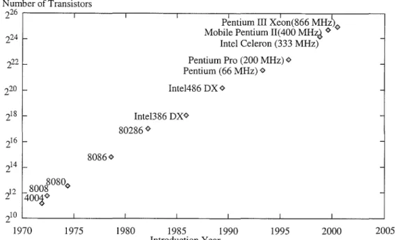
In 1947, the age of semiconductors arrived with the development of the first junction transistors by William Shockley and his colleagues in Bell Labs of United States. The semi-conductor transistors have great advantage over the traditional electromagnetic switching devices in size, speed, power dissipation and reliability etc. In 1958, the world's first inte-grated circuits (ICs) was developed by Jack Kilby in Texas Instruments where transistors, resistors and capacitors along with their interconnecting wiring were fabricated on a single piece of Germanium and glued to a glass slide. From then on, the integrated circuit technol-ogy has progressed tremendously. In 1961, commercial ICs became available from Fairchild Instruments. Four years later, Gordon Moore, co-founder of Intel, predicted that the num-ber of transistors on a chip of integrated circuits could be doubled every 12 to 18 months. His statement can still be validated by Intel microprocessors as show in fig.1.2[101]. Un-fortunately, most of the classical methods of logic minimization are only suitable for small Boolean functions. Therefore, these logic design methods must be improved to meet the rapid growth of the semiconductor technology.
Although there are only several theorems in Boolean algebra to simplify Boolean func-tions, the obtained results of minimization largely depend on how to select the orders of these theorems and to which terms to apply them[84]. For large Boolean functions, there are too many alternatives to be considered exhaustively. In 1976, the first general survey of Boolean function complexity was introduced in [129]. Following that there was immense research on the complexity of Boolean networks and their realizations that can be found in
Chapter 1. Introduction Section 1.2
N umber of Transistors
226 ,---r---,---,---,---,---,---,
P~ntium III Xeon(866 MHz)<> Mobile Pentium 11(400 MHz~ <> 8086<> Intel Celeron (333 MHz) Pentium Pro (200 MHz) <> Pentium (66 MHz) <> Intel486 DX <> Inte1386 DX<> 80286 <> 210 ~ ______ L -_ _ _ _ _ _ ~ _ _ _ _ _ _ ~ _ _ _ _ _ _ _ IL_ ______ L_I ______ ~I ______ ~ 1970 1975 1980 1985 1990 1995 2000 2005 Introduction Year
*
These data are originally from "Intel Microprocessor Quick Reference Guide"Figure 1.2: Moore's law - the growth of Intel microprocessors
[57J. It was realized that neither the traditional methods of switching theory nor manual design was feasible for large functions. With the development of automatic physical design methods for large Boolean systems[115, 123], several heuristic and efficient methods have been applied to obtain "good" solutions for large Boolean functions with the aid of com-puters. This process is typically called logic optimization or logic synthesis that was first commercially available in 1980's[131]. Recently the designs of systems-on-a-chips (SOCs) started to attract more and more organizations that lead to urgent demand for new genera-tion logic synthesis tools[76]. In July of 1997, logic synthesis tools for designing Applicagenera-tion Specific Integrated Circuits (ASICs) and SOCs became available[13]. Expert systems may be a new facility for logic synthesis[132]. Besides, Linux has been recommended to be a new common operating system in EDA communities because it is the only candidate offering a compatibility for both workstations and personal computers (PCs)[133].
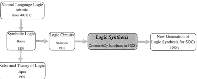
On the other hand, there is a new challenge for Symbolic Logic proposed in Japan. In their opinion, the current prevailing theory of Symbolic Logic needs a thorough revision because of some crucial misunderstanding. Their newly developed theory is available in the electronic book of Internet, Elements of the Reformed Theory of Logic[136]. It will not be discussed here since this topic is beyond the coverage of this thesis. The above historic perspective can be shown in fig.1.3, where "logic synthesis" is the subject of this thesis.
Chapter 1. Introduction
Natural Language Logic
Aristotle about 400 B.C. Symbolic Logic Boole Japan 1997 Circuits 1938
Figure 1.3: Historic perspective of logic design
Section 1.2
New Generation of Logic Synthesis for SOCs
1990's
1.2 VLSI chip design methodology based on logic synthesis
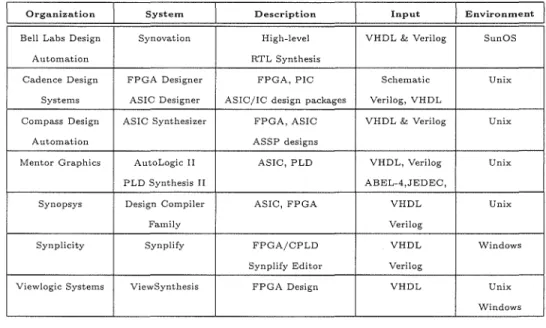
The wide range of computer-aided design (CAD) tools for digital integrated circuits can fall into four major categories based on the production of Very Large Scale Integration (VLSI) components[59]: memories, microprocessors, Application Specific Integrated Cir-cuits (ASICs), and Programmable Logic Devices (PLDs)[29, 108, 124]. Numerous indus-trial applications can be implemented by either ASICs or field programmable gate arrays (FPGAs) and offer distinct advantages. Besides, countless commercial design synthesis tools are available and some of them are shown in table 1.1. Today's ASICs have a low cost-per-gate advantage as well as an inherent speed advantage. In contrast, FPGAs have been winning with their time-to-market and reprogrammability. This detail analysis and prediction of the competition between ASICs and FPGAs is addressed in [14]. Additionally, it can be seen that VHDL[113] and Verilog[140] are the most popular hardware description languages (HDLs ). Furthermore, each company usually applies different design methodol-ogy. However, a unified model of design representation has been developed in [149]. It is proposed that a model of design representation can be described by three separate do-mains, namely behavioral, structural, and physical domains. Behavioral domain describes the basic functionality of the design while structural domain the abstract implementation, and the physical domain the physical implementation of the design. Each domain can further be divided into five abstract levels that are architectural, algorithmic, register & transfer, logic and circuit levels. This design model can be represented in fig.1.4 that is quite similar to Y-chart in [65].Based on the model in fig. 1.4, design synthesis is the process of translating a high abstract level in the behavioral domain to a low level in the physical domain through structural domain. Different design methodology may take different tracks on this model. Moreover, not all the levels in this three domains need to be fitted neatly. For example, silicon compilation can generate physical layout directly from behavioral description[15].
Chapter 1. Introduction Section 1.2
Organization System Description Input Environment
Bell Labs Design Synovation High-level VHDL & Verilog SunOS
Automation RTL Synthesis
Cadence Design FPGA Designer FPGA, PIC Schematic Unix Systems ASIC Designer ASIC/IC design packages Verilog, VHDL
COlllpass Design ASIC Synthesizer FPGA, ASIC VHDL & Verilog Unix
Automation ASSP designs
Mentor Graphics AutoLogic II ASIC, PLD VHDL, Verilog Unix
PLD Synthesis II ABEL-4,JEDEC,
Synopsys Design Compiler ASIC, FPGA VHDL Unix
Family Verilog
Synplicity Synplify FPGA/CPLD VHDL Windows
Synplify Editor Verilog
Viewlogic Systems ViewSynthesis FPGA Design VHDL Unix Windows
Table 1.1: Some commercial design synthesis tools
Architectural Level
Behavioral
Structural
L Floorplans Clusters hysical PartitionPhysical
Figure 1.4: A VLSI design model
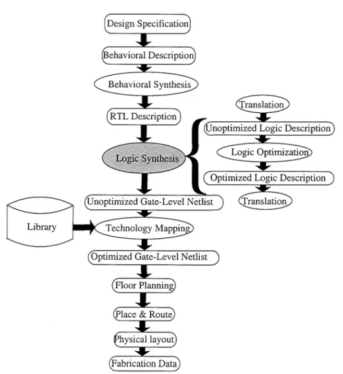
A typical ASIC chip design flow based on logic synthesis can be shown in fig.1.5. It can be seen from fig.1.5 that three steps are involved in logic synthesis:
Chapter 1. Introduction Section 1.3
Library
Figure 1.5: An ASIC chip design flow
gates, flip-flops, and latches. The description file in logic level may be in the formats of KISS (Keep Internal State Simple), BLIF (Berkeley Logic Interchange Format), SLIF (Stanford Logic Interchange Format), PLA(Programmable Logic Array), and equations. All these formats can be converted to each other by Sr8[134].
2. Optimize the description through various available procedures by the criteria of area, speed, power dissipation[19], or testability. This important process is typically called logic optimization. Recently adiabatic circuits based on split-level charge recovery logic(SCRL) is a new topic for low power VLSI design[62].
3. Produce a gate level net-list, usually in electronic design interchange format (EDIF)[58]. Comparatively speaking, step 2 is the most difficult one. In the last two decades, a lot of heuristic techniques have been developed for logic minimization of large Boolean functions and circuits. A new multilevel logic optimization method, based on functional don't cares (DCs), will be proposed according to the criterion of area in chapter 3 and 4 of this thesis.
Chapter 1. Introduction Section 1.3
1.3 Two-Level versus
multilevel logic
synthesis
In the logic level of design synthesis, the two-level logic minimization is a mature and very popular approach especially for control logic. Quine[117] laid down the basic theory that was adapted later by McCluskey[96], known as Quine-McCluskey procedure. It basically consists of two steps:
1. Generate all the prime implicants from on-set minterms of a Boolean function; 2. Select an optimal subset of these primes that cover all the on-set minterms of the
function.
Even though the primes can be efficiently produced in [78], solving the covering problem is known as an NP-complete problem. Thus this technique becomes impractical for large Boolean functions. The next important contribution in this area is MINI[78] that was further developed into ESPREsso[26], the most powerful and popular two-level minimizer up to date. It is possible for ESPRESSO to find "very good" solutions for incompletely specified functions with hundreds of inputs and outputs in a reasonable time. There is one main loop consisting of four main procedures in ESPRESSO, EXPAND, ESSENTIAL_PRIME, IRREDUNDANT _ COVER, and REDUCE. EXPAND replaces the previous cubes by prime implicants and assures the cover is minimal with respect to single-cube containment. Then· ESSENTIAL _ PRIME extracts the essential primes and put them in the don't care set. Following that IRREDUNDANT _ COVER find an optional minimum irredundant cover by deleting totally redundant cubes. Finally, REDUCE procedure reduce all the cubes to be smallest that cover only necessary on-set minterms. Although REDUCE produces a non-prime cover, it can facilitate improvement in the subsequent iterations over the local minimum result obtained by IRREDUNDANT _ COVER.
Two-level logic and its Programmable Logic Array (PLA) implementations shown in fig.1.6(a) provide good solutions to a wide class of problems in logic design. However, there are situations, especially for large multiple output circuits, where multilevel design is desirable and more effective. It facilitates sharing and simplifies testing. For example, a simple logic circuit,
(1.1) which can be shown in fig.1.6(b), has three levels. In the first level, the product term XOX3 is generated, which is an AND level. In the second level, both (XOX3
+
X2) and(xo
+
Xl) are generated with an OR level. Finally, they are combined by an AND gate to produce the output for the function. Additionally, multilevel realization is useful for both control and data-flow logic[25]. However, multilevel logic circuits are much more difficult to be synthesized than two-level circuits. In 1964, Lawler proposed an approach for exactChapter 1. Introduction Inputs Programmable Array of AND gates Product terms Programmable Array of OR gates Outputs
(a) Two-Level programmable logic array (PLA) structure
(b) A simple example for multilevel logic circuit
Figure 1.6: Comparison between two-level and multilevel structures
Section 1.4
multilevel logic minimization[90]. All the multilevel prime implicants are first generated, then a minimal subset is found by solving a covering problem using any method for two-level minimization. As an exact optimization method, it is only suitable for small Boolean functions on account of high computational complexity. In the last two decades, many heuristic techniques have been developed that will be reviewed in chapter 2.
1.4 Reed-Muller logic based on AND /XOR operations
It was presented in the classic paper [135], published in 1938, that any n-variable Boolean function
f
can be expanded by Shannon expansion based on AND/OR operations asChapter 1. Introduction Section 1.4
follows.
(1.2) where 0 :::; i :::; n-1, and !Xi=O and !Xi=l are called the cofactors of! with respect to Xi.
Alternatively, any Boolean function can be represented based on AND jXOR operations, which is called Reed-Muller expansion[103, 119]. In contrast to equation (1.2), there are
three basic expansions using AND jXOR operations, which are shown in equations (1.3) -(1.5).
!(Xn-lXn-l ... xo) = XdXi=O EB XdXi=l (1.3)
(1.4)
(1.5)
In logic synthesis process, Reed-Muller logic methods are important alternatives to
the traditional SOP approaches to implement Boolean functions. Currently, the widely used logic minimizers for SOP forms, such as ESPREsso[26] and 8rs[134] are based on the "unate paradigm", according to which most of the Boolean functions of practical interest are close to unate and nearly unate functions. While the category of unate and nearly unate functions covers many control and glue logic circuits, these minimizers perform quite poorly on other broad classes of logic[154]. For instance, the unateness principle does not work well for arithmetic circuits, digital signal processing operations, linear or nearly linear functions, and randomly generated Boolean logic functions[72, 126]. However, Reed-Muller realization is especially suitable for these functions[2, 46]. For example, to represent a parity function with n variables, ! = xOEBxl EB· . ·EBxn-l, an SOP form needs 2n-1 product terms while only n terms are sufficient for an AND jXOR expression. Additionally, circuits based on ANDjXOR operations have great advantage of easy testability [44, 92, 118].
Applications of Reed-Muller logic to function classification[143], Boolean matching[144]' and symmetry detection[145] have also been achieved.
Due to the lack of an efficient Reed-Muller logic minimizer, applications of Reed-Muller implementations have not become popular despite these advantages. It is generally ac-cepted that the optimization problem for Reed-Muller logic is much more difficult than the standard Boolean logic. One of the main obstacles is the polarity problem, including
Chapter 1. Introduction Section 1.5
fixed polarity and mixed polarity, which does not exist in SOP forms for the standard Boolean logic. For a fixed polarity Reed-Muller (FPRM) form, the number of product terms largely depends on the polarity for the same function. Further, any Boolean function can be represented canonically by FPRM forms while it does not hold for mixed polarity expressions. Conventionally, Boolean functions are represented by AND/OR operations, instead of AND /XOR operations. Thus, the optimization of Reed-Muller logic consists of conversion algorithm between SOP and FPRM formats, fixed polarity and mixed polarity minimization. These will be discussed in chapters 5 to 8.
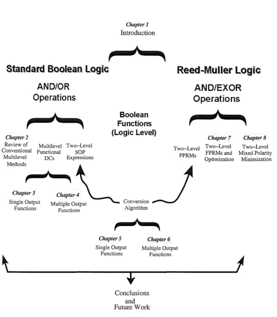
1.5 Structure of this thesis
Any Boolean function can be represented by two paradigms, which are based on AND/OR and AND /XOR operations respectively. Correspondingly, there are two main parts in this thesis as shown in fig. 1.7. The first part is multilevel logic minimization based on AND/OR operations. The conventional methods for multilevel logic synthesis are reviewed in chapter 2 based on AND/OR operations. A new type of don't cares (DCs), functional DCs, are introduced comparing with satisfiability DCs and observability DCs. The usefulness of functional DCs is discussed for single output functions in chapter 3 and for multiple output functions in chapter 4 respectively. The second part deals with Reed-Muller logic which is based on AND /XOR operations. A mutual conversion algorithm is first proposed to convert a single output Boolean function between SOP and FPRM formats in chapter 5 and for very large multiple output functions in chapter 6 respectively. There are 2n polarities for
an n-variable function, and the number of on-set product terms largely depends on the polarity. Therefore a fast algorithm in presented in chapter 7 to find the best polarity for a function, which corresponds with the least number of on-set product terms. This FPRM form with the best polarity can be further simplified with respect to the number of product terms by combining the adjacent terms. Consequently, the result is in mixed polarity Reed-Muller forms, which is covered in chapter 8. Finally, the main improvements and contributions are summarized and some future work is suggested in the "conclusions and future work".
Chapter 1. Introduction Chapter 1 Introduction
.... ..,+"' ....
f'
,
Section 1.5Standard Boolean logic
ANDIOR
Operations
Reed .. Muner Logic
AND/EXOR Operations
f
Chapter 2
Review of Multilevel Two-Level Conventional Functional SOP
Multilevel DCs Expressions Boolean Functions (Logic Level)
f
+z
Chapter 7 Two-Level Two-Level PPRMs FPRMs and MethodsL
J
C/""~'4
Single Output Multiple Output Conversion
Optimization
Functions Functions Algorithm
ChapterS Chapter 6 Single Output Multiple Output
Chapter 8 Two-Level Mixed Polarity Minimization Functions Functions
~'--
_ _ _ _ _ _
----J'
t
Conclusions and Future WorkPPRMs: positive polarity Reed-Muller expressions FPRMs: fixed polarity Reed-Muller expressions
Chapter 2
Conventional Multilevel Logic
Synthesis
2.1
Algorithmic approach
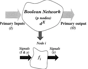
The algorithmic approach to multilevel logic optimization consists of defining an algorithm for each transformation type, including elimination, decomposition, extraction, factoring, and substitution. These transformations are manipulated based on the concept of Boolean networks[74J.
Definition 2.1. A Boolean network 'T/ for n-variable m-output functions is an
intercon-nection of p Boolean functions defined by a five-tuple (f, y, 1,0, dX), consisting of:
1.
f
= (fo,il," .
,fp-d,
a vector of completely specified logic functions. Each of them is a node in the network.2. Y = (Yo, Y1,'" ,Yp-1), a vector of logic variables (signals of the network) where Yi
has a one-to-one correspondence with
fi,
0 ::; i ::; p - 1. In other words, the output of anode can be an input for other nodes.
3. 1= (10,
h,' .. ,In-d,
a vector of externally controllable signals as primary inputs. 4. 0 = (0o, 01 , ... ,Om-d,
a vector of externally observable signals as primary out-puts.5. dX = (di, df,··· ,d~_d, a vector of completely specified logic functions that specify the set of don't care minterms on the outputs of'T/ where X
=
Yr.For combinational logic functions, a Boolean network is usually equivalent to a Directed Acyclic Graph (DAG) as show in fig.2.1. Elimination, collapsing or flattening of an internal node of a Boolean network is its removal from the network, resulting in a network with one less nodes. Decomposition is the process of re-expressing a node as a number of sub-nodes so that these sub-nodes may be shared by other nodes in the network. Extraction, related to decomposition, is the process of creating a new common sub-node for several interme-diate nodes in the network. Consequently, the structure of all these intermeinterme-diate nodes
Chapter 2. Conventional Multilevel Approaches Section 2.1
are simplified. The optimization problem associated with the extraction transformation is to identify a set of common sub-nodes such that the resulting network has minimum area, delay, power dissipation, maximum testability or routability[41]. If the sum-of-products form of Boolean functions are considered as polynomial expressions, rather than Boolean expressions, then factoring the common polynomial terms will lead to a simpler structure of the corresponding network. The factoring problem is how to find a factored form with the minimum number of literals. Substitution or resubstitution, is the inverse transforma-tion of eliminatransforma-tion. It creates an arc in the Boolean network connecting the node of the substituting function to the node of the substituted function[50, 100].
(p nodes)
d X
Nodei
Primary output
(0)
Figure 2.1: DAG representation of a combinational Boolean network
Among these transformations, division operation, the inverse process of product op-eration, plays a very important role to identify a common sub-expression. Given two expressions, F and P, find expressions Q and R, such that F
=
p. Q+
R, where Q and R'are quotient and remainder respectively. If "." and
"+"
are taken as algebraic operations, then this is algebraic division, or weak division; otherwise, if they are taken as Boolean operations, then this is Boolean division. Comparatively speaking, algebraic division is faster but neglects other useful properties of Boolean algebra except distribute law. How-ever, due to the lack of an efficient algorithm, Boolean division has rarely been applied[37]. A widespread concept of kernel is first proposed in 1982 based on algebraic division as follows[24].Definition 2.2. The kernels of an expression F for a Boolean function
f
are the set ofK(F),
Chapter 2. Conventional Multilevel Approaches Section 2.2
where
D(F) = {Fie I e is a eube}
and g is cube free means that there is no cube to divide it evenly and
"I"
is algebraic division.Example 2.1. A four-variable completely specified function f(x3x2x1xo) = ~{O, 1,2,5,8,
9, 10} has a minimal two-level expression F1 as follows,
(2.1) In equation (2.1), Xo +X1, X2 +X3XO are the kernels[24] so that F1 can be simplified to
F2 or F3 by algebraic division in equations (2.2) or (2.3).
(2.2) and
(2.3) Both equations (2.2) and (2.3) are not the minimal multilevel forms because this func-tion
f
can also be expressed by F4 using Boolean division in equation (2.4).(2.4) In addition to algebraic division technique, another facility that is extensively used is don't care method, including both satisfiability don't cares (SDC) and observability don't cares (ODC)[17, 130] in the logic level although there are more DCs in high level synthesis[20, 23]. These DCs are shown as dX in fig.2.1. Generally, SDCs and ODCs are quite large and complex[38]. Hence filters are needed to reduce the size so that only the useful portions are retained[125].
Within Mrs[27] that was further developed into Srs[134], there are many algorithms to compute the kernels and realize the previous five types of transformations. Additionally, some scripts are included in Srs to obtain good results for different kinds of functions. Extensive experimental results for Srs have been reported in [1].
Chapter 2. Conventional Multilevel Approaches Section 2.3
2.2
Rule-Based approach
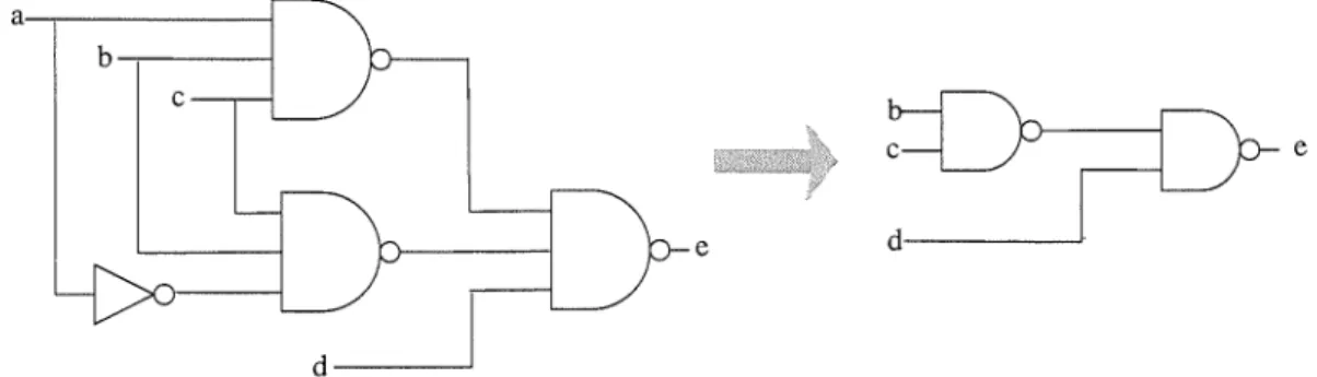
Rule-based systems are a class of expert systems that use a set of rules to determine the action to be taken to minimize a Boolean network[18, 47]. The network undergoes local transformations[48] that preserve its functionality by a stepwise refinement.
A rule-based system may consist of[100]:
I.-
A rule database that contains two types of rules: replacement rules and meta-rules. The former abstract the local knowledge about subnetwork replacement and the latter the global heuristic knowledge about the convenience of using a particular strategy(i.e. applying a set. of replacement rules).
I.-
A system for entering and maintaining the database.I.-
A controlling mechanism that implements the inference engine.A rule database contains a family of circuit patterns and the corresponding replacement for both replacement rules and meta-rules according to the overall goal, such as optimizing area, speed, power dissipation or testability. Several rules may match a pattern, and a priority scheme is used to choose the replacement. For example, a circuit pattern is shown in fig.2.2, when it is acknowledged by the rule-based system, it will be replaced by a smaller circuit. a - ; - - - / b - . - - - - i c e
d~
Figure 2.2: A circuit pattern and its replacement
A major advantage of this approach is that rules can be added to the database to cover all thinkable replacements and particular design styles. This feature plays a key role in the acceptance of optimization systems, because when a designer could outsmart the program, the new knowledge pattern could then be translated into a rule and incorporated into the database.
The major disadvantage in the rule-based system is the order in which rules should be applied and the possibility of look-ahead and backtracking. This is the task of the control algorithm, that implements the inference engine. Further discussion and experimental results can be found in [18, 47, 66].
Chapter 2. Conventional Multilevel Approaches Section 2.3
2.3 BDD approach
Binary Decision Diagrams (BDDs) were first proposed as Binary-Decision programs (BDPs) in 1959[91], which are further generalized by Akers in 1978 and represented them as diagrams[12]. Early research results can be found in [102]. Any Boolean function can be expressed by a BDD based on the following definition[31].
Definition 2.3. A BDD is a rooted directed graph with vertex set V containing two
kinds of vertices, terminal and nonterminal vertices. If a vertex is a terminal vertex, then it is associated a value of either 0 or 1 denoted as value( v) E {O, I}; otherwise, if it is a nonterminal vertex then it has as attribute an argument index, index( v) E
{a,
1, ... ,n -I}and two children, low(v), high(v) E V. An n-variable Boolean function
I
can be expressed by the value of the root vertex. Any vertex v corresponds with a Boolean functionIv
defined recursively as:
1) If v is a terminal vertex:
a) Ifvalue(v) =1, then
Iv
= 1; b) Ifvalue(v) =0, thenIv
= 0.2) If v is a nonterminal vertex with index(v) = i, then
Iv
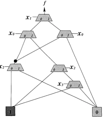
is the functionIv = xdzow(v)
+
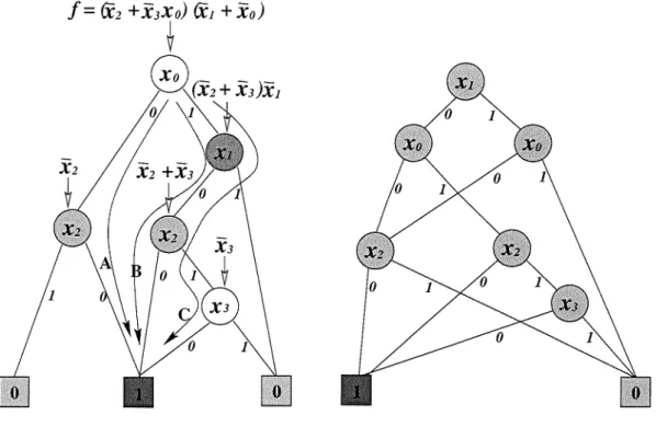
Xdhigh(v) (2.5)In example 2.1, a Boolean function I(X3X2XIXO) = I:{O, 1,2,5,8,9, 10} can also be ex-pressed by a BDD as in fig.2.3(a) corresponding with equation (2.4). Each path from the root vertex to any terminal vertex corresponds to either an on-set or off-set product term. In fig.2.3(a), there are three paths A, Band C, from the root vertex to "I" terminal ver-tex. They correspond to three on-set products, X2XO, X2XIXO, and X3X2XIXO respectively. Putting these products together leads to another form F5 of this function
f.
(2.6)
Notice there are two common edges between path Band C. Thus another multilevel form can be obtained as follows.
(2.7) There are several operations directly manipulated on BDDs, RESTRICTION, COMPOSI-TION, SATISFY, and ApPLY etc[31]. The most complex operation is ApPLY through which
Chapter 2. Conventional Multilevel Approaches Section 2.3
(a) with variable order (xO,xl,x2,x3) (b) with variable order (xl,xO,x2,x3)
Figure 2.3: BDD representation of the Boolean function in example 2.1
two BDDs, G1 and G2 are combined as one BDD, G
=
G1 <op> G2 where op is anyBoolean operation.
A BDD can be simplified by the following two rules: 1. If low(v) = high(v), then v can be deleted;
2. If the subgraphs rooted by v and Vi are isomorphic, then v and Vi can be merged to
one vertex.
A reduced BDD that has been simplified by these two rules is unique for any Boolean function if the variable order is fixed[31]. In fig.2.3(b), another BDD is shown for the same function as in fig.2.3( a) but with different variable order. It can be seen that fig.2.3(b) has one more vertex than fig.2.3(a). The unique BDD corresponding with a fixed variable order is called reduced ordered BDD(ROBDD). Therefore, the equivalence of two Boolean functions can be checked through ROBDDs. This technique has been incorporated into S18[134].
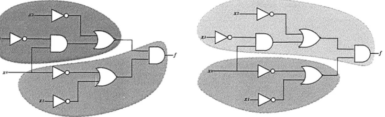
A logic circuit can be constructed from a BDD if each node is replaced by a multi-plexor(MUX). The circuit corresponding with fig.2.3(b) is shown in fig.2.4.
A BDD with less node number corresponds with a simpler logic circuit realized with MUXes. Hence the minimization of the number of nodes of a BDD is quite important[109].
Chapter 2. Conventional Multilevel Approaches Section 2.4
f
Figure 2.4: Logic circuit from fig.2.3(b)
Unfortunately, the size of a BDD, that is its node number, is very sensitive to the ordering of variables. There have been extensive research on the variable ordering of BDDs[7, 9-11, 16, 34, 55, 80, 110, 122, 159]. Furthermore, some functions do not produce efficient results when processed using BDDs. For example, the sizes of the BDDs for representing arithmetic functions such as multiplication are known to increase exponentially with the number of input variables[75]. Therefore, a lot of other formats of decision diagrams, such as reversed ROBDDs[32], hybrid DDs[40], output value array graphs(OVAG)[82], edge-valued BDDs[89] and partitioned ROBDDs [107]' have been proposed for different types of Boolean functions that were surveyed in [30, 52]. The research on testability for BDDs can be found in [33].
2.4 FPGA approach
The first type of user-programmable chip that could implement Boolean functions was the Programmable Read-Only Memory(PROM) introduced at the beginning of 1970s. Simple logic functions can be created using PROMs as a look-up table which stores the truth table of the function. The function inputs are connected to the address lines and the function truth table is programmed into the memory array for each function output. Field-Programmable Logic Array(FPLA) or simply PLA, shown as in fig.1.6(a), was later developed specially for implementing large logic circuits by Signetics in 1975, where both AND and OR planes are programmable. In section 1.3, it is discussed that multilevel
Chapter 2. Conventional Multilevel Approaches Section 2.4
logic networks usually offer more general structures and better solutions for large com-plex circuits. Therefore, Field-Programmable Gate Array (FPGA) was first introduced by the Xilinx company in 1985[139] to meet the general multilevel structures. FPGAs have much more density on a chip than PLAs with the technological evolution while the reprogramming time and cost are drastically reduced comparing with mask programmable gate arrays(MPGAs). The FPGA market has expanded dramatically with many differ-ent competing designs, developed by companies including Actel, Advanced Micro Devices, Algotronix, Altera, AT&T, Cypress, Intel, Lattice, Motorola, Quick Logic, and Texas In-struments etc. A generic FPGA architecture, shown in fig.2.5, consists of an array of logic elements together with an interconnect network which can be configured by the user at the point of application. This kind architecture has a very good correspondence with the definition of Boolean network in fig.2.1. Each node in the Boolean network is mapped into a logic block while the interconnection among the nodes can be configured inside a FPGA. Hence, user programming specifies both the logic function of each block and the connections between the blocks. The programming technologies used in commercial FPGA products include floating gate transistors, anti-fuses, and Static Random Access Memory (SRAM) cells. A brief comparison among these programming techniques is shown in table2.1[83].
Technique EPROM EEPROM Anti Fuse SRAM Configurable Block Configurable
Figure 2.5: Typical FPGA architecture
Volatile Series Relative
Storage Resistance(O) Capacitance
no 2K 10 no 2K 10 no 50-500 1.2-5.0 yes 1K 15 Relative Cell Area 1 2 1 5 Table 2.1: Brief comparison of FPGA programming techniques
Chapter 2. Conventional Multilevel Approaches Section 2.5
The design flow for FPGA chip is different from fig.1.5. Taking an example of Xilinx XACT design system, the description file after logic synthesis must first be translated into Xilinx Net-list Format (XNF), which is understood by Xilinx tools. Then in the technology mapping step, the XNF file is mapped into Xilinx Configurable Logic Blocks (CLBs). This step is very important because a Boolean network can be mapped into different CLBs based on different partitions. In fig.2.6, a Boolean network is partitioned into two different
CLBs that lead different structure and cost in FPGA realizations. There has been a lot of research in this area, merging logic optimization with technology mapping[41]. In the next
step, automatic placement assigns each CLB a physical location on the chip using simulated annealing algorithm. After the physical placement and routing (P&R) is completed, a BIT
file is then created which contains the binary programming data. The final step is to download the BIT file to configure the SRAM bits of the target chip. Since all the logic
blocks have been prefabricated on the chip, FPGA designs have been winning over ASICs with its time-to-market, low NRE(non-recurring engineering) fees, and reprogrammable features[14]' especially for small volume of products.
Figure 2.6: Different partitions for the same Boolean network
2.5
Several other approaches based on perturbation
There are some other methods for exploiting don't cares in Boolean networks. Muroga proposed transduction method, an acronym for transformation and reduction, based on the concept of permissible functions[105]. If replacing a node of function
f
in a Boolean network with another node of function 9 applying DCs of the network does not change the output, then 9 is called a permissible function forf.
After the replacement, the network can be transformed either locally or globally so that some redundant part in the network can be removed. These transformations and reductions are repeated until no further improvement is possible without changing the network outputs. These ideas were employed in the design. system, SYLON[106] for CMOS circuit design.The idea of logic perturbation by rearranging the structure of the network without affecting its behavior, has been further applied for both combinational and sequential
Chapter 2. Conventional Multilevel Approaches Section 2.5
circuits[45]. With the help of efficient automatic test pattern generation (ATPG) tech-niques, redundancy addition and removal method was proposed based on perturbation in [39]. Some other results about perturbation can be found in [160, 161].
Chapter 3
Multilevel Logic Minimization Using
Functional Don't Cares
3.1 Introduction
Multilevel logic synthesis is a known difficult problem although it can produce better re-sults than two-level logic synthesis methods. In [90], multilevel prime implicants are first generated from a Boolean function, then a minimal form of these prime implicants is selected by solving a covering problem using any method for conventional two-level min-imization. As an exact optimization method, it is only suitable for small functions due to the high computational complexity. In the last two decades, many heuristic methods have been proposed[24-25, 37, 50-51, 74, 100, 134, 160-161]. In most algorithmic methods, algebraic division plays an important role to decompose a function. Unfortunately, alge-braic division applies the distribute law only, neglecting other useful properties of Boolean algebra. Besides, DCs can not be used[100]. As for its counterpart, Boolean division, there is no effective algorithm to find a good divisor. To compute the quotient for a given divisor, a large amount of implicit don't cares, SDCs(satisfiability don't cares) and ODCs( observability don't cares) should be generated and then a two-level minimizer[50J is used. This approach has rarely been used because of its complexity[37, 51]. Moreover, both of these kinds of divisions depend largely on the initial expressions[25]. Consequently, there are different standard scripts, as used in Sr8[134], that can give quite different results for the same problem. Sometimes, further running a script may deteriorate the result. Other Boolean methods can be found in [25, 74, 87, 100, 160J.
Traditionally, the systematic approach to multilevel logic synthesis is known as func-tional decomposition[43J. The main problem with this approach is to find the minimum column multiplicity for a bound set of variables based on simple disjunctive decomposition, multiple disjunctive decomposition and some more complicated decomposition methods [112]. A renewed interest in functional decomposition is caused by the introduction of
Chapter 3. Functional DCs for Single Output Functions Section 3.2
Look-Up table FPGAs recently[41]. There, a given switching function is broken down into a number of smaller subfunctions so that it can be implemented by the basic blocks of the FPGAs.
The DCs discussed in this chapter are based on the functionality while the implicit SDCs and ODCs are based on the topology of a Boolean network. In addition, these functional DCs are different from the DCs generated on variable-entered Karnaugh maps[2, 71]. A new efficient method to apply these functional DCs for multilevel logic synthesis is proposed according to a criterion based on the number of literals.
3.2 Multilevel Karnaugh map technique
Any Boolean function can be decomposed by Shannon expansion as follows,
f =
xdlxi=l
+
xdlxi=O (Xi+
flxi=O)(Xi+
flxi=r)(3.1) (3.2) where flxi=O and flxi=l are the cofactors of f with respect to Xi and Xi. In the Karnaugh map, the effect of the decomposition of equation (3.1) is to split the map into two sub-maps of equal dimensions covered by cubes Xi and Xi. The split is applied recursively until no off-set is covered based on the different orders of variables. All these cubes of the sub-maps are linked by the OR operation which leads to the expression of the function. This is the traditional two-level Karnaugh map technique where no DCs are generated after the selection of a cube[2]. It is similar to the decomposition of equation (3.2). The main purpose for two-level logic minimization is to find the least number of cubes and literals in each cube, that is equivalent to the best order of variables to decompose the function. For example, f(X3X2XIXO) = 2:(2,3,5,7,11,13,15) is shown in fig.3.1(a), where the blank entries on the map are "0" outputs. Splitting this map recursively with respect to Xo and Xl leads to a cube XIXO, which covers no off-set but 4 on-set minterms. Similarly, splitting this map recursively with respect to
xo,
X2 and Xl, X2, X3 respectively leads to two cubesX2XO and X3X2XI, which covers no off-set but all the remaining on-set minterms. Therefore, this function can be expressed by linking these three cubes with the "OR" operation as in equation (3.3).
(3.3) In the previous two-level minimization, no DCs are generated. Actually, after the selec-tion of a cube, all the on-sets covered by this cube can be used as DCs for the subsequent minimization. This idea will be generalized to multilevel cubes as will be shown in
defini-Chapter 3. Functional DCs for Single Output Functions Section 3.2
tion 3.1 and will consequently lead to multilevel forms. In [93], a concept of pseudocube is presented that has a more general form than the two-level cube since the XOR operation is incorporated. Any arbitrary Boolean function can then be expressed as a three-level, AND-XOR-OR form that has less literal number than the standard two-level form of sum of products(SOP) in general. A pseudo cube enjoys some useful properties but still covers "I" entries only on a Karnaugh map. In this chapter, the concept of a cube on a Karnaugh map is generalized in the following definition.
Definition 3.1. A multilevel cube on a Karnaugh map is the same as a two-level cube
except that it can cover both "0" and "I" entries, where "DC" is used to indicate a don't care minterm which can be either "0" or "I".
Definition 3.2. A Karnaugh map M will produce its complemented Karnaugh map M'
by interchanging the entries of "0" and "I" while DCs remain the same.
Theorem 3.1. Given a Karnaugh map of an incompletely specified single output n-variable
k
function f(x n-l,xn-2,"'xo), and a multilevel cube c
=
ITxi=
XkXk-l"'XO, that may i=Ocover the entries of "1 ", "0" and "DC", 0 ::; k ::; n-1, Xi E {Xi, Xi}, Xi E {Xn-l, Xn-2, ... xo}, then f can be decomposed as in equation (3.4) or (3.5).
f
ch+12 Xk'" xlxoh+
12 Xk ... xlxo13+
12 f (c+
f4)f5 = (Xk'" XIXO+
f4)f5 = (Xk'" XIXO+
16)f5 (3.4) (3.5)In equation (3.4), h is a function of n-k-l variables whose Karnaugh map is exactly the n-k-l dimensional sub-map that is inside cube c; the Karnaugh map of 12 is the same as M except that any entry of "1" covered by cube c can be taken as "DC"; and the Karnaugh map of
13
is the complemented Karnaugh map of h. In equation (3.5), f4 is the function whose Karnaugh map is exactly the sub-map covered by cubec;
the Karnaugh map ofis
is the same as M except that any entry of "0" covered by cubec
can be taken as "DC"; and the Karnaugh map of f6 is the complemented Karnaugh map of f4·Proof. We will proof equation (3.4) only since equation (3.5) is the dual form of equation (3.4). Moreover, in equation (3.4) only f
=
Xk ... xlxoh+
12 needs proving on account of definition 3.2.Chapter 3. Functional DCs for Single Output Functions
Part A: entries that are inside cube c; Part B: entries that are outside cube c.
Section 3.2
If all these entries of "I" are covered, then
1
is realized. From the definitions of hand12,
all "I" entries in part A are covered bych,
all "I" entries in part B are covered by12.
Now we need to prove thath
doesn't include any variables in c.Because
°
AND x = 0, x E {O, 1, DC}, all the entries outside of cube c on the map can be used as DCs while minimizing functionh.
Suppose there is a term, xjF, in the two-level SOP expression of 11, X j is a literal of the variable x j, j E {O, 1, .. , ,k}, then there must be a cubexjF
that is outside cubexjF,
whose entries can be used as DCs on the Karnaugh map. Let all these DCs inside the cubexjF
be "I" so that we havexjF
+
xjF
=F.
Therefore, deletingXj
fromxjF
will not change the functionch.
From this point,h
doesn't include any variable in c. In other words, the Karnaugh map ofh
is exactly the n-k-l dimensional sub-map that is inside cube c.When all the "I" entries inside cube c have been covered by
ch,
they can be considered to be DCs for minimizing12
since 1+
x = 1, x E {O, 1, DC}.o
Example 3.1. Equation (3.3) is the minimal two-level expression without the aid of DCs
for the function shown in fig.3.1(a). Now, apply theorem 3.1 to obtain the multilevel expressions utilizing DCs of functional decomposition. Suppose a multilevel cube Xo is selected first that covers both "0" and "I" entries. Then
1
can be expressed as follows based on equation (3.4),1
=
xoh
+
12
(3.6)where
h,
as shown in fig.3.1(c), is a three variable function, independent of Xo. Further-more, all the "I" entries covered byxoh
can be used as DCs that are entries of" x" in fig.3.1(d) to minimize12.
Selecting a multilevel cube X2X1 that covers "0" entries only leads to the expressionh
=
X2X1=
X2+
Xl as in fig.3.1(c). Additionally, cube X3X2X1 in fig.3.1(d) covers the only on-set minterm. Therefore, we have(3.7) Alternatively, when the multilevel cube Xo is selected in fig.3.1(b), equation (3.5) can be applied to split the map. Hence,
Chapter 3. Functional DCs for Single Output Functions
10
(a) two-level K-map method
x2xl 10 (c) K-map for f1 x 3X-,-,,-0---,-_ DO * 01 11 10 *
(e) K-map for f4
x IXO
Iff
3X2 00 01 I 10 00 I I 01 I I II I I 10 I(b) select a multilevel cube
x
~
IXO 3X2 00 01 I 10 00 x I 01 x x II x x 10 x (d) K-map forf2 IxO x 3x_ 00 01 11 10 00 x 1 1 01 x 1 1 x 11 x 1 1 x 10 x 1 x (f) K-map for f5 Section 3.2Figure 3.1: Comparison between two-level and multilevel K-map methods
and all the "0" entries covered by
c
can be used as DCs for15.
Hence, the Karnaugh maps for14
and15
are shown in fig.3.1(e) and (f). Therefore we have another expression for1
as follows.1
(xo+
X3 X2Xl)X2 Xl(xo
+
X3X2Xl)(X2+
Xl)If the property of "containment" of cofactors, which will be discussed in the next section, is applied, two new "DC" entries for