INTERNATIONAL TELECOMMUNICATION UNION
ITU-T
V.90
TELECOMMUNICATION STANDARDIZATION SECTOR OF ITU(09/98)
SERIES V: DATA COMMUNICATION OVER THE
TELEPHONE NETWORK
Simultaneous transmission of data and other signals
A digital modem and analogue modem pair
for use on the Public Switched Telephone
Network (PSTN) at data signalling rates of
up to 56 000 bit/s downstream and up to
33 600 bit/s upstream
ITU-T Recommendation V.90
ITU-T V-SERIES RECOMMENDATIONS
DATA COMMUNICATION OVER THE TELEPHONE NETWORK
For further details, please refer to ITU-T List of Recommendations.
General V.1–V.9
Interfaces and voiceband modems V.10–V.34
Wideband modems V.35–V.39
Error control V.40–V.49
Transmission quality and maintenance V.50–V.59
Simultaneous transmission of data and other signals V.60–V.99
Interworking with other networks V.100–V.199
Interface layer specifications for data communication V.200–V.249
Control procedures V.250–V.299
ITU-T RECOMMENDATIONS SERIES
Series A Organization of the work of the ITU-TSeries B Means of expression: definitions, symbols, classification Series C General telecommunication statistics
Series D General tariff principles
Series E Overall network operation, telephone service, service operation and human factors Series F Non-telephone telecommunication services
Series G Transmission systems and media, digital systems and networks Series H Audiovisual and multimedia systems
Series I Integrated services digital network
Series J Transmission of television, sound programme and other multimedia signals Series K Protection against interference
Series L Construction, installation and protection of cables and other elements of outside plant Series M TMN and network maintenance: international transmission systems, telephone circuits,
telegraphy, facsimile and leased circuits
Series N Maintenance: international sound programme and television transmission circuits Series O Specifications of measuring equipment
Series P Telephone transmission quality, telephone installations, local line networks Series Q Switching and signalling
Series R Telegraph transmission
Series S Telegraph services terminal equipment Series T Terminals for telematic services Series U Telegraph switching
Series V Data communication over the telephone network
Series X Data networks and open system communications Series Y Global information infrastructure
Series Z Programming languages
Printed in Switzerland Geneva, 1999ITU-T RECOMMENDATION V.90
A DIGITAL MODEM AND ANALOGUE MODEM PAIR FOR USE
ON THE PUBLIC SWITCHED TELEPHONE NETWORK (PSTN)
AT DATA SIGNALLING RATES OF UP TO 56 000 bit/s
DOWNSTREAM AND UP TO 33 600 bit/s UPSTREAM
Summary
This Recommendation specifies the operation of a digital modem and analogue modem pair for use on the Public Switched Telephone Network (PSTN) at data signalling rates of up to 56 000 bit/s in the downstream direction and up to 33 600 bit/s in the upstream direction. The two modems are specified herein in terms of coding, start-up signals and sequences, operating procedures and DTE-DCE interface functionalities. The network interface of the digital modem and the signalling rate that is used to connect the digital modem locally to a digital switched network are considered to be national matters and are hence not specified herein.
Source
ITU-T Recommendation V.90 was prepared by ITU-T Study Group 16 (1997-2000) and was approved under the WTSC Resolution No. 1 procedure on the 25th of September 1998.
FOREWORD
ITU (International Telecommunication Union) is the United Nations Specialized Agency in the field of telecommuni-cations. The ITU Telecommunication Standardization Sector (ITU-T) is a permanent organ of the ITU. The ITU-T is responsible for studying technical, operating and tariff questions and issuing Recommendations on them with a view to standardizing telecommunications on a worldwide basis.
The World Telecommunication Standardization Conference (WTSC), which meets every four years, establishes the topics for study by the ITU-T Study Groups which, in their turn, produce Recommendations on these topics.
The approval of Recommendations by the Members of the ITU-T is covered by the procedure laid down in WTSC Resolution No. 1.
In some areas of information technology which fall within ITU-T’s purview, the necessary standards are prepared on a collaborative basis with ISO and IEC.
NOTE
In this Recommendation the term recognized operating agency (ROA) includes any individual, company, corporation or governmental organization that operates a public correspondence service. The terms Administration, ROA and public
correspondence are defined in the Constitution of the ITU (Geneva, 1992).
INTELLECTUAL PROPERTY RIGHTS
The ITU draws attention to the possibility that the practice or implementation of this Recommendation may involve the use of a claimed Intellectual Property Right. The ITU takes no position concerning the evidence, validity or applicability of claimed Intellectual Property Rights, whether asserted by ITU members or others outside of the Recommendation development process.
As of the date of approval of this Recommendation, the ITU had received notice of intellectual property, protected by patents, which may be required to implement this Recommendation. However, implementors are cautioned that this may not represent the latest information and are therefore strongly urged to consult the TSB patent database.
ITU 1999
All rights reserved. No part of this publication may be reproduced or utilized in any form or by any means, electronic or mechanical, including photocopying and microfilm, without permission in writing from the ITU.
CONTENTS
Page 1 Scope ... 1 2 References ... 1 3 Definitions ... 2 4 Abbreviations ... 4 5 Digital modem ... 55.1 Data signalling rates... 5
5.2 Symbol rate ... 5
5.3 Scrambler ... 5
5.4 Encoder ... 5
5.4.1 Mapping parameters ... 5
5.4.2 Input bit parsing ... 6
5.4.3 Modulus encoder ... 6 5.4.4 Mapper ... 7 5.4.5 Spectral shaping ... 7 5.4.6 Sign assignment... 10 5.4.7 Mux ... 10 6 Analogue modem... 10
6.1 Data signalling rates... 11
6.2 Symbol rates... 11 6.3 Carrier frequencies ... 11 6.4 Pre-emphasis ... 11 6.5 Scrambler ... 11 6.6 Framing ... 11 6.7 Encoder ... 11 7 Interchange circuits... 11
7.1 List of interchange circuits... 11
7.2 Asynchronous character-mode interfacing... 11
8 Start-up signals and sequences ... 11
8.1 Phase 1 ... 12
8.2 Phase 2 ... 12
8.2.1 A ... 12
8.2.2 B ... 12
8.2.3 INFO sequences ... 12
8.2.4 Line probing signals ... 16
8.3 Phase 3 signals for the analogue modem ... 16
8.3.1 Ja ... 17 8.3.2 MD ... 20 8.3.3 PP ... 20 8.3.4 S... 20 8.3.5 SCR ... 20 8.3.6 TRN... 20
8.4 Phase 3 signals for the digital modem... 20
8.4.1 DIL ... 20
8.4.2 Jd ... 21
8.4.3 Jd′ ... 21
8.4.4 Sd... 21
Page
8.5 Phase 4 signals for the analogue modem ... 22
8.5.1 B1 ... 22
8.5.2 CP ... 22
8.5.3 E ... 25
8.6 Phase 4 signals for the digital modem... 25
8.6.1 B1d ... 26 8.6.2 Ed ... 26 8.6.3 MP ... 26 8.6.4 R ... 27 8.6.5 TRN2d... 28 9 Operating procedures... 28
9.1 Phase 1 – Network interaction ... 28
9.1.1 Use of bits in Recommendation V.8... 28
9.1.2 Call modem ... 29
9.1.3 Answer modem... 29
9.2 Phase 2 – Probing/ranging ... 29
9.2.1 Digital modem... 30
9.2.2 Analogue modem ... 31
9.3 Phase 3 – Equaliser and echo canceller training and digital impairment learning ... 32
9.3.1 Digital modem... 32
9.3.2 Analogue modem ... 34
9.4 Phase 4 – Final training... 34
9.4.1 Digital modem... 35 9.4.2 Analogue modem ... 36 9.5 Retrains ... 36 9.5.1 Digital modem... 36 9.5.2 Analogue modem ... 36 9.6 Rate renegotiation ... 37 9.6.1 Digital modem... 37 9.6.2 Analogue modem ... 38 9.7 Cleardown ... 39 10 Testing facilities ... 39 11 Glossary ... 40 Appendix I – Overview ... 41
Recommendation V.90
Recommendation V.90 (09/98)
A DIGITAL MODEM AND ANALOGUE MODEM PAIR FOR USE
ON THE PUBLIC SWITCHED TELEPHONE NETWORK (PSTN)
AT DATA SIGNALLING RATES OF UP TO 56 000 bit/s
DOWNSTREAM AND UP TO 33 600 bit/s UPSTREAM
(Geneva, 1998)
1
Scope
This Recommendation specifies the operation between two different modems, one a digital modem and the other an analogue modem, both as defined in clause 3. The two modems are specified herein in terms of coding, start-up signals and sequences, operating procedures and DTE-DCE interface functionalities. The network interface of the digital modem and the signalling rate that is used to connect the digital modem locally to a digital switched network are considered to be national matters and are hence not specified herein. The principal characteristics of these modems are as follows:
a) duplex mode of operation on the PSTN;
b) channel separation by echo cancellation techniques;
c) PCM modulation in the downstream direction at a symbol rate of 8000;
d) synchronous channel data signalling rates in the downstream direction from 28 000 bit/s to 56 000 bit/s in increments of 8000/6 bit/s;
e) V.34 modulation in the upstream direction;
f) synchronous channel data signalling rates in the upstream direction from 4800 bit/s to 28 800 bit/s in increments of 2400 bit/s, with optional support for 31 200 bit/s and 33 600 bit/s;
g) adaptive techniques that enable the modems to achieve close to the maximum data signalling rates the channel can support on each connection;
h) negotiate full duplex V.34 operation if a connection will not support V.90 operation; i) exchange of rate sequences during start-up to establish the data signalling rate;
j) automoding to V-series modems supported by V.32 bis automode procedures and group 3 facsimile machines; k) use of V.8, and optionally V.8 bis, procedures during modem start-up or selection.
2
References
The following Recommendations contain provisions which, through reference in this text, constitute provisions of this Recommendation. At the time of publication, the editions indicated were valid. All Recommendations are subject to revision; all users of this Recommendation are therefore encouraged to investigate the possibility of applying the most recent editions of the Recommendations listed below. A list of currently valid ITU-T Recommendations is regularly published.
– CCITT Recommendation G.711 (1988), Pulse Code Modulation (PCM) of voice frequencies.
– ITU-T Recommendation T.30 (1996), Procedures for document facsimile transmission in the general switched
telephone network.
– ITU-T Recommendation V.8 (1998), Procedures for starting sessions of data transmission over the public switched
telephone network.
– ITU-T Recommendation V.8 bis (1996), Procedures for the identification and selection of common modes of
operation between Data Circuit-terminating Equipments (DCEs) and between Data Terminal Equipments (DTEs) over the public switched telephone network and on leased point-to-point telephone-type circuits.
– ITU-T Recommendation V.14 (1993), Transmission of start-stop characters over synchronous bearer channels. – ITU-T Recommendation V.24 (1998), List of definitions for interchange circuits between Data Terminal
Equipment (DTE) and Data Circuit-terminating Equipment (DCE).
– ITU-T Recommendation V.25 (1996), Automatic answering equipment and general procedures for automatic
calling equipment on the general switched telephone network including procedures for disabling of echo control devices for both manually and automatically established calls.
– CCITT Recommendation V.32 bis (1991), A duplex modem operating at data signalling rates of up to 14 400 bit/s
for use on the general switched telephone network and on leased point-to-point 2-wire telephone-type circuits.
– ITU-T Recommendation V.34 (1998), A modem operating at data signalling rates of up to 33 600 bit/s for use on
the general switched telephone network and on leased point-to-point 2-wire telephone-type circuits.
– ITU-T Recommendation V.42 (1996), Error-correcting procedures for DCEs using asynchronous-to-synchronous
conversion.
– ITU-T Recommendation V.43 (1998), Data flow control.
– ITU-T Recommendation V.80 (1996), In-band DCE control and synchronous data modes for asynchronous DTE .
3
Definitions
This Recommendation defines the following terms:
3.1 analogue modem: The analogue modem is the modem of the pair that, when in data mode, generates V.34
signals and receives G.711 signals that have been passed through a G.711 decoder. The modem is typically connected to a PSTN.
3.2 digital modem: The digital modem is the modem of the pair that, when in data mode, generates G.711 signals
and receives V.34 signals that have been passed through a G.711 encoder. The modem is connected to a digital switched network through a digital interface, e.g. a Basic Rate Interface (BRI) or a Primary Rate Interface (PRI).
3.3 downstream: Transmission in the direction from the digital modem towards the analogue modem.
3.4 nominal transmit power: Reference transmit power that is configured by the user.
3.5 Uchord: Ucodes are grouped into eight Uchords. Uchord1 contains Ucodes 0 to 15; Uchord2 contains Ucodes
16 to 31; …; and Uchord8 contains Ucodes 112 to 127.
3.6 Ucode: The universal code used to describe both a µ-law and an A-law PCM codeword. All universal codes are given in decimal notation in Table 1. The µ-law and A-law codewords are the octets to be passed to the digital interface by the digital modem and are given in hexadecimal notation. All modifications defined in Recommen-dation G.711 have already been made. The MSB in the µ-law PCM and A-law PCM columns in Table 1 corresponds to the polarity bit of the G.711 character signals. A linear representation of each PCM codeword is also given.
Table 1/V.90 – The universal set of PCM codewords Ucode µ-law PCM µ-law linear A-law PCM A-law linear Ucode µ-law PCM µ-law linear A-law PCM A-law linear 0 FF 0 D5 8 64 BF 1980 95 2112 1 FE 8 D4 24 65 BE 2108 94 2240 2 FD 16 D7 40 66 BD 2236 97 2368 3 FC 24 D6 56 67 BC 2364 96 2496 4 FB 32 D1 72 68 BB 2492 91 2624 5 FA 40 D0 88 69 BA 2620 90 2752 6 F9 48 D3 104 70 B9 2748 93 2880 7 F8 56 D2 120 71 B8 2876 92 3008 8 F7 64 DD 136 72 B7 3004 9D 3136 9 F6 72 DC 152 73 B6 3132 9C 3264 10 F5 80 DF 168 74 B5 3260 9F 3392 11 F4 88 DE 184 75 B4 3388 9E 3520 12 F3 96 D9 200 76 B3 3516 99 3648 13 F2 104 D8 216 77 B2 3644 98 3776 14 F1 112 DB 232 78 B1 3772 9B 3904 15 F0 120 DA 248 79 B0 3900 9A 4032 16 EF 132 C5 264 80 AF 4092 85 4224 17 EE 148 C4 280 81 AE 4348 84 4480 18 ED 164 C7 296 82 AD 4604 87 4736 19 EC 180 C6 312 83 AC 4860 86 4992 20 EB 196 C1 328 84 AB 5116 81 5248 21 EA 212 C0 344 85 AA 5372 80 5504 22 E9 228 C3 360 86 A9 5628 83 5760 23 E8 244 C2 376 87 A8 5884 82 6016 24 E7 260 CD 392 88 A7 6140 8D 6272 25 E6 276 CC 408 89 A6 6396 8C 6528 26 E5 292 CF 424 90 A5 6652 8F 6784 27 E4 308 CE 440 91 A4 6908 8E 7040 28 E3 324 C9 456 92 A3 7164 89 7296 29 E2 340 C8 472 93 A2 7420 88 7552 30 E1 356 CB 488 94 A1 7676 8B 7808 31 E0 372 CA 504 95 A0 7932 8A 8064 32 DF 396 F5 528 96 9F 8316 B5 8448 33 DE 428 F4 560 97 9E 8828 B4 8960 34 DD 460 F7 592 98 9D 9340 B7 9472 35 DC 492 F6 624 99 9C 9852 B6 9984 36 DB 524 F1 656 100 9B 10364 B1 10496 37 DA 556 F0 688 101 9A 10876 B0 11008 38 D9 588 F3 720 102 99 11388 B3 11520 39 D8 620 F2 752 103 98 11900 B2 12032
Table 1/V.90 – The universal set of PCM codewords (concluded)
4
Abbreviations
This Recommendation uses the following abbreviations: BRI Basic Rate Interface
DCE Data Circuit-terminating Equipment DIL Digital Impairment Learning sequence DTE Data Terminal Equipment
PRI Primary Rate Interface
PSTN Public Switched Telephone Network RMS Root Mean Square
RTDEa Round-Trip Delay Estimate – Analogue modem RTDEd Round-Trip Delay Estimate – Digital modem UINFO The Ucode given by bits 25:31 of INFO1a
Ucode µ-law PCM µ-law linear A-law PCM A-law linear Ucode µ-law PCM µ-law linear A-law PCM A-law linear 40 D7 652 FD 784 104 97 12412 BD 12544 41 D6 684 FC 816 105 96 12924 BC 13056 42 D5 716 FF 848 106 95 13436 BF 13568 43 D4 748 FE 880 107 94 13948 BE 14080 44 D3 780 F9 912 108 93 14460 B9 14592 45 D2 812 F8 944 109 92 14972 B8 15104 46 D1 844 FB 976 110 91 15484 BB 15616 47 D0 876 FA 1008 111 90 15996 BA 16128 48 CF 924 E5 1056 112 8F 16764 A5 16896 49 CE 988 E4 1120 113 8E 17788 A4 17920 50 CD 1052 E7 1184 114 8D 18812 A7 18944 51 CC 1116 E6 1248 115 8C 19836 A6 19968 52 CB 1180 E1 1312 116 8B 20860 A1 20992 53 CA 1244 E0 1376 117 8A 21884 A0 22016 54 C9 1308 E3 1440 118 89 22908 A3 23040 55 C8 1372 E2 1504 119 88 23932 A2 24064 56 C7 1436 ED 1568 120 87 24956 AD 25088 57 C6 1500 EC 1632 121 86 25980 AC 26112 58 C5 1564 EF 1696 122 85 27004 AF 27136 59 C4 1628 EE 1760 123 84 28028 AE 28160 60 C3 1692 E9 1824 124 83 29052 A9 29184 61 C2 1756 E8 1888 125 82 30076 A8 30208 62 C1 1820 EB 1952 126 81 31100 AB 31232 63 C0 1884 EA 2016 127 80 32124 AA 32256
5
Digital modem
5.1 Data signalling rates
Synchronous channel data signalling rates from 28 000 bit/s to 56 000 bit/s in increments of 8000/6 bit/s shall be supported. The data signalling rate shall be determined during Phase 4 of modem start-up according to the procedures described in 9.4.
5.2 Symbol rate
The downstream symbol rate shall be 8000 established by timing from the digital network interface. The digital modem shall support the upstream symbol rates 3000 and 3200. It may also support the optional upstream symbol rate 3429 as defined in Recommendation V.34.
5.3 Scrambler
The digital modem shall include a self-synchronizing scrambler as specified in clause 7/V.34, using the generating polynomial, GPC, in equation 7-1/V.34.
5.4 Encoder
The block diagram in Figure 1 is an overview of the encoder and represents one data frame. Data frames in the digital modem have a six-symbol structure. Each symbol position within the data frame is called a data frame interval and is indicated by a time index, i = 0, …, 5, where i = 0 is the first in time. Frame synchronization between the digital modem transmitter and analogue modem receiver is established during training procedures.
T1604730-98/d01 Ki Ui Mi Ci Ui tj(n) b0 : bK–1 s0 : sS–1 d0 : dD–1 pj(n) $0 : $5 Sr Modulus encoder Mi-point map Assign signs Mux Serial PCM octets Bit parser parse to shaping frames Differential encoder Spectral shaper
Figure 1/V.90 – Digital modem encoder block diagram
PCMi
FIGURE 1/V.90...[D01] = 3 CM 5.4.1 Mapping parameters
Mapping parameters, established during training or rate renegotiation procedures, are:
– six PCM code sets, one for each data frame interval 0 to 5, where data frame interval i has Mi members;
– K, the number of modulus encoder input data bits per data frame;
– Sr, the number of PCM code sign bits per data frame used as redundancy for spectral shaping; and
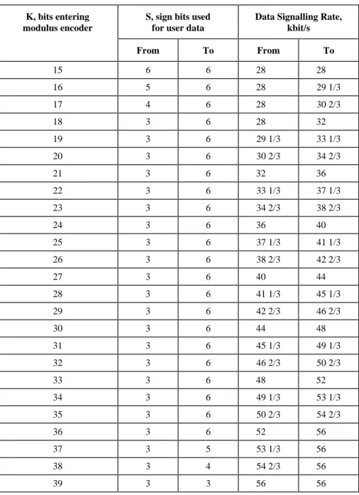
Table 2 shows the data signalling rates achieved by the valid combinations of K and S during data mode. Table 17 shows the valid combinations of K and S used during Phase 4 and rate renegotiation procedures.
Table 2/V.90 – Data signalling rates for different K and S
5.4.2 Input bit parsing
D (equal to S + K) serial input data bits, d0 to dD–1 where d0 is first in time, are parsed into S sign input bits and
K modulus encoder bits. d0 to dS–1 form s0 to sS–1 and dS to dD–1 form b0 to bK–1.
The K modulus encoder bits and the S sign bits are used as specified in 5.4.3 and 5.4.5 respectively.
5.4.3 Modulus encoder
K bits enter the modulus encoder. The data signalling rates associated with each value of K are tabulated in Table 2. There are six independent mapping moduli, M0 to M5, which are the number of members in the PCM code sets defined
for data frame interval 0 to data frame interval 5, respectively. Mi is equal to the number of positive levels in the
constellation to be used in data frame interval i as signalled by the analogue modem using the CP sequences defined in 8.5.2.
K, bits entering modulus encoder
S, sign bits used for user data
Data Signalling Rate, kbit/s From To From To 15 6 6 28 28 16 5 6 28 29 1/3 17 4 6 28 30 2/3 18 3 6 28 32 19 3 6 29 1/3 33 1/3 20 3 6 30 2/3 34 2/3 21 3 6 32 36 22 3 6 33 1/3 37 1/3 23 3 6 34 2/3 38 2/3 24 3 6 36 40 25 3 6 37 1/3 41 1/3 26 3 6 38 2/3 42 2/3 27 3 6 40 44 28 3 6 41 1/3 45 1/3 29 3 6 42 2/3 46 2/3 30 3 6 44 48 31 3 6 45 1/3 49 1/3 32 3 6 46 2/3 50 2/3 33 3 6 48 52 34 3 6 49 1/3 53 1/3 35 3 6 50 2/3 54 2/3 36 3 6 52 56 37 3 5 53 1/3 56 38 3 4 54 2/3 56 39 3 3 56 56
The values of Mi and K shall satisfy the inequality 2K Mi i ≤ =
∏
0 5The modulus encoder converts K bits into six numbers, K0 to K5, using the following algorithm.
NOTE – Other implementations are possible but the mapping function must be identical to that given in the algorithm described below.
1) Represent the incoming K bits as an integer, R0:
R0 = b0 + b1*21 + b2*22 + ... + bK–1*2K–1
2) Divide R0 by M0. The remainder of this division gives K0, the quotient becomes R1 for use in the calculation for the next data frame interval. Continue for the remaining five data frame intervals. This gives K 0 to K5 as:
Ki = Ri modulo Mi, where 0 ≤ Ki < Mi; Ri+1 = (Ri – Ki) / Mi
3) The numbers K0, …, K5 are the output of the modulus encoder, where K0 corresponds to data frame interval 0 and K5 corresponds to data frame interval 5.
5.4.4 Mapper
There are six independent mappers associated with the six data frame intervals. Each mapper uses a tabulation of Mi
PCM codes that make up the positive constellation points of data frame interval i denoted Ci. The PCM codes to be used
in each data frame interval are specified by the analogue modem during training procedures. The PCM code that is denoted by the largest (smallest) Ucode is herein called the largest (smallest) PCM code. The members of Ci shall be
labelled in descending order so that label 0 corresponds to the largest PCM code in Ci, label Mi – 1 corresponds to the
smallest PCM code in Ci. Each mapper takes Ki and forms Ui by choosing the constellation point in Ci labelled by Ki.
5.4.5 Spectral shaping
The digital modem output line signal spectrum shall be shaped, if spectral shaping is enabled. Spectral shaping only affects the sign bits of transmitted PCM symbols. In every data frame of 6 symbol intervals, Sr sign bits are used as
redundancy for spectral shaping while the remaining S sign bits carry user information. The redundancy, Sr, is specified
by the analogue modem during training procedures and can be 0, 1, 2 or 3. When Sr=0, spectral shaping is disabled.
NOTE – The initial state of the spectral shaper does not affect the performance of the analogue modem and is therefore left to the implementor.
5.4.5.1 Sr= 0, S = 6
The PCM code sign bits, $0 to $5 shall be assigned using input sign bits s0 to s5 and a differential coding rule:
$0 = s0 ⊕ ($5 of the previous data frame); and
$i = si ⊕ $i–1 for i = 1, ..., 5
where "⊕" stands for modulus-2 addition.
5.4.5.2 Sr= 1, S = 5
Sign bits s0 to s4 shall be parsed to one six-bit shaping frame per data frame according to Table3.
Table 3/V.90 – Parsing input sign bits to shaping frames
Table 4/V.90 – Odd bit differential coding
Finally, a second differential encoding shall be performed to produce the initial shaping sign bit assignment, tj(0) to tj(5) using the rule:
t (k) = p (k) tj ′j ⊕ j–1(k)
The spectral shaper converts each bit tj(k), to a PCM code sign bit $k as described in 5.4.5.5.
5.4.5.3 Sr= 2, S = 4
Sign bits s0 to s3 shall be parsed to two three-bit shaping frames per data frame as shown in Table 3.
The odd bit in each shaping frame shall be differentially encoded to produce differentially encoded outputs p′j
and pj+1′ according to Table 4.
Finally, a second differential encoding shall be performed on each shaping frame to produce the initial shaping sign bit assignments tj(0) to tj(2) and tj+1(0) to tj+1(2) using the differential encoding rule:
tj(k) = p (k)′j ⊕ tj–1(k)
tj+1(k) = p′j+1(k) ⊕ t (k)j
The spectral shaper converts each bit tj(k), to PCM code sign bit $k and each bit tj+1(k), to PCM code sign bit $k+3 as
described in 5.4.5.5.
5.4.5.4 Sr= 3, S = 3
Sign bits s0 to s2 shall be parsed to three two-bit shaping frames per data frame as shown in Table 3.
The odd bit in each shaping frame shall be differentially encoded to produce differentially encoded outputs p′j, p′j+1,
and pj+2′ as shown in Table 4. Data frame interval Sr= 1, S =5 Sr= 2, S =4 Sr= 3, S = 3 0 pj(0) =0 pj(0) =0 pj(0) = 0 1 pj(1) = s0 pj(1) = s0 pj(1) = s0 2 pj(2) = s1 pj(2) = s1 pj+1(0) = 0 3 pj(3) = s2 pj+1(0) =0 pj+1(1) = s1 4 pj(4) = s3 pj+1(1) = s2 pj+2(0) = 0 5 pj(5) = s4 pj+1(2) = s3 pj+2(1) = s2 Data frame interval Sr = 1, S = 5 Sr = 2, S = 4 Sr = 3, S = 3 0 p (0) ′j =0 p (0) j′ =0 p (0) ′j =0 1 p (1) p (1) pj′ = j ⊕ ′j –1(5) p (1) p (1) pj′ = j ⊕ ′j –1(1) p (1) p (1) pj′ = j ⊕ ′j –1(1) 2 p (2) p (2)′j = j p (2) p (2)′j = j p′j+1(0) =0 3 p (3)′j = p (3)j ⊕ ′p (1)j p′j+1(0) =0 p′j+1(1) = pj+1 (1) p (1)⊕ ′j 4 p (4) p (4)j′ = j p′j+1(1) = pj+1 (1) ⊕ ′ p (1)j p′j+2(0) = 0 5 p (5) = p (5)j′ j ⊕ ′p (3)j p′j+1(2) = pj+1(2) p′j+2(1) = pj+2(1) p⊕ ′j+1(1)
Finally, a second differential encoding shall be performed on each shaping frame to produce the initial shaping sign bit assignments tj(0) to tj(1), tj+1(0) to tj+1(1), and tj+2(0) to tj+2(1) using the differential encoding rule:
tj(k) = p (k)j′ ⊕ tj–1(k)
tj+1(k) = p′j+1(k) ⊕ t (k)j
tj+2(k) = p′j+2(k) ⊕ tj+1(k)
The spectral shaper converts each bit tj(k), to PCM code sign bit $k, each bit tj+1(k), to PCM code sign bit $k+2, and each
bit tj+2(k), to PCM code sign bit $k+4 as described in 5.4.5.5.
5.4.5.5 Spectral shaper
The spectral shaper operates on a spectral shaper frame basis. For the cases Sr= 2 and Sr= 3, there are multiple shaper
frames per six-symbol data frame. Spectral shaper operation for each shaper frame within a data frame (called shaping frame j in this subclause) is identical except that they affect different data frame PCM sign bits as shown in Table 5.
Table 5/V.90 – Shaping frame to data frame sign relationship
The spectral shaper shall modify the initial sign bits [tj(0), tj(1), …] to corresponding PCM code sign bits ($0, $1 …)
without violating the constraint described below, so as to optimize a spectral metric.
The constraint of the spectral shaper is described using the 2-state trellis diagram shown in Figure 2.
T1604740-98/d02 A D C B state 0 state 1
Figure 2/V.90 – Trellis diagram used to constrain the spectral shaper
FIGURE 2/V.90...[D02] = 3 CM
In a given spectral shaping frame j, the spectral shaper shall modify the initial sign sequence, tj(k), according to one of
the following four sign inversion rules: – Rule A: Do nothing;
– Rule B: Invert all sign bits in spectral shaping frame j;
– Rule C: Invert even-numbered [tj(0), tj(2), etc.] sign bits in spectral shaping frame j;
– Rule D: Invert odd-numbered [tj(1), tj(3), etc.] sign bits in spectral shaping frame j. Data frame interval Sr= 1, S =5 Sr= 2, S =4 Sr= 3, S = 3 Data frame PCM sign bit 0 tj(0) tj(0) tj(0) $0 1 tj(1) tj(1) tj(1) $1 2 tj(2) tj(2) tj+1(0) $2 3 tj(3) tj+1(0) tj+1(1) $3 4 tj(4) tj+1(1) tj+2(0) $4 5 tj(5) tj+1(2) tj+2(1) $5
The trellis diagram describes the sequence of sign inversion rules that are allowable. For example, when the spectral shaper is in state Qj= 0 at the beginning of frame j, only rules A and B are allowable in frame j. The current state Qj
together with the sign inversion rule selected for frame j determine the next state Qj+1 according to the trellis diagram. The look-ahead depth parameter, ld, is an integer between 0 and 3 selected by the analogue modem during training procedures. Id of 0 and 1 are mandatory in the digital modem. Id of 2 and 3 are optional.
To select the sign inversion rule for the jth spectral shaping frame, the spectral shaper shall use the PCM symbol
magnitudes produced by the mapper for spectral shaping frames j, j+1, ..., j+ld. It shall compute the spectral metric that would result if each of the allowable sequences of sign inversion rules for frames j through j+ld, starting from the current state Qj in frame j, were to be used. The shaper shall select the sign inversion rule for frame j that minimizes the spectral
metric, w[n], defined in 5.4.5.6 up to and including the final symbol of spectral shaping frame j+ld. The selection determines the next state Qj+1.
The shaper shall then set PCM code signs $i for shaping frame j according to the selected sign inversion rule for shaper
frame j.
5.4.5.6 Spectral shape filter
The analogue modem determines the spectral shape filter function used in the digital modem by selecting parameters of the following transfer function:
T z a z a z b z b z ( ) ( )( ) ( )( ) –1 = − − − − − − − 1 1 1 1 1 2 1 1 1 2 1
where a1, a2, b1 and b2 are parameters having absolute values less than or equal to 1. The parameters, a1, a2, b1 and b2
are specified by the analogue modem during training procedures and are represented in the 8-bit two’s-complement format with 6 bits after the binary point. The digital modem shall perform the spectral shaping according to the spectral shaping metric, w[n], characterised by the filter:
F z T z b z b z a z a z ( ) ( ) ( )( ) ( )( ) –1 = = − − − − − − − 1 1 1 1 1 1 2 1 1 1 2 1
The filter input, x[n], shall be a signed signal proportional to the linear value corresponding to PCM codes being transmitted. The relationship between PCM codes and corresponding linear values is given in Table 1. w[n] shall be computed as:
1) y[n] = x[n] – b1x[n–1] + a1y[n–1]
2) v[n] = y[n] – b2y[n–1] + a2v[n–1]
3) w[n] = v2[n] + w[n–1]
5.4.6 Sign assignment
Six sign bits, generated by 5.4.5, are attached to the six unsigned mapper outputs U0 – U5 to complete the mapping of
the data frame intervals. A sign bit of 0 means the transmitted PCM codeword will represent a negative voltage and a sign bit of 1 means it will represent a positive voltage.
5.4.7 Mux
The signed PCM codewords, PCMi, are transmitted from the digital modem sequentially with PCM0 being first in time.
6
Analogue modem
The characteristics of the analogue modem described herein apply when in V.90 mode. After fallback to V.34 mode, the analogue modem shall have characteristics as defined in Recommendation V.34.
6.1 Data signalling rates
The modem shall support synchronous data signalling rates of 4800 bit/s to 28 800 bit/s in increments of 2400 bit/s, with optional support for 31 200 bit/s and 33 600 bit/s. The 200 bit/s V.34 auxiliary channel is not supported. The data signalling rate shall be determined during Phase 4 of modem start-up according to the procedures described in 9.4.
6.2 Symbol rates
The analogue modem shall support the symbol rate 3200. It may also support 3000 and the optional symbol rate 3429 as defined in Recommendation V.34. The other V.34 symbol rates, 2400, 2743 and 2800, shall not be supported. The symbol rate shall be selected by the analogue modem during Phase 2 of modem start-up according to the procedures described in 9.2.
6.3 Carrier frequencies
The analogue modem shall support the carrier frequencies specified in 5.3/V.34 for the appropriate symbol rate. The carrier frequency shall be determined during Phase 2 of modem start-up according to the procedures specified in 9.2.
6.4 Pre-emphasis
The analogue modem shall support the pre-emphasis filter characteristics specified in 5.4/V.34. The filter selection shall be provided by the digital modem during Phase 2 of modem start-up according to the procedures specified in 9.2.
6.5 Scrambler
The analogue modem shall include a self-synchronizing scrambler as specified in clause 7/V.34, using the generating polynomial, GPA, in equation 7-2/V.34.
6.6 Framing
The analogue modem shall use the framing method specified for the V.34 primary channel in clause 8/V.34.
6.7 Encoder
The analogue modem shall use the encoder specified for the V.34 primary channel in clause 9/V.34.
7
Interchange circuits
The requirements of this clause apply to both modems.
7.1 List of interchange circuits
References in this Recommendation to V.24 interchange circuit numbers are intended to refer to the functional equivalent of such circuits and are not intended to imply the physical implementation of such circuits. For example, references to circuit 103 should be understood to refer to the functional equivalent of circuit 103 (see Table 6).
7.2 Asynchronous character-mode interfacing
The modem may include an asynchronous-to-synchronous converter interfacing to the DTE in an asynchronous (or start-stop character) mode. The protocol for the conversion shall be in accordance with Recommendation(s) V.14, V.42 or V.80. Data compression may also be employed.
8
Start-up signals and sequences
Table 6/V.90 – Interchange circuits
8.1 Phase 1
Recommendation V.8, and optionally Recommendation V.8 bis, is used in Phase 1. All signals in 9.1 are defined in either Recommendation V.25 or Recommendation V.8 and shall be transmitted at the nominal transmit power level.
8.2 Phase 2
During Phase 2, all signals except L1 shall be transmitted at the nominal transmit power level. If a recovery mechanism returns the modem to Phase 2 from a later phase, the transmit level shall revert to the nominal transmit power from the previously negotiated transmit power level.
8.2.1 A
As defined in 10.1.2.1/V.34.
8.2.2 B
As defined in 10.1.2.2/V.34.
8.2.3 INFO sequences
INFO sequences are used to exchange modem capabilities, results of line probing, and data mode modulation parameters.
8.2.3.1 Modulation
All INFO sequences are transmitted using binary DPSK modulation at 600 bit/s ± 0.01%. The transmit point is rotated 180 degrees from the previous point if the transmit bit is a 1, and the transmit point is rotated 0 degrees from the previous point if the transmit bit is a 0. Each INFO sequence is preceded by a point at an arbitrary carrier phase. When multiple INFO sequences are transmitted as a group, only the first sequence is preceded by a point at an arbitrary carrier phase.
INFO sequences are transmitted by the analogue modem with a carrier frequency of 2400 Hz ± 0.01%, at 1 dB below the nominal transmit power, plus an 1800 Hz ± 0.01% guard tone 7 dB below the nominal transmit power. INFO sequences are transmitted by the digital modem with a carrier frequency of 1200 Hz ± 0.01% at the nominal transmit power. The transmitted line signal shall have a magnitude spectrum within the limits shown in Figure 13/V.34.
Interchange circuit
No. Description Notes
102 103 104 105 106
Signal ground or common return Transmitted data
Received data Request to send Ready for sending 107
108/1 or 108/2 109
Data set ready Connect data set to line Data terminal ready
Data channel received line signal detector 1 125
133
Calling indicator
Ready for receiving 2
NOTE 1 – Thresholds and response times are not applicable because a line signal detector cannot be expected to distinguish received signals from talker echoes.
NOTE – It is highly desirable to design linear phase transmitter channel separation and shaping filters since there are no provisions for adaptive equaliser training.
8.2.3.2 INFO information bits
The CRC generator used is described in 10.1.2.3.2/V.34.
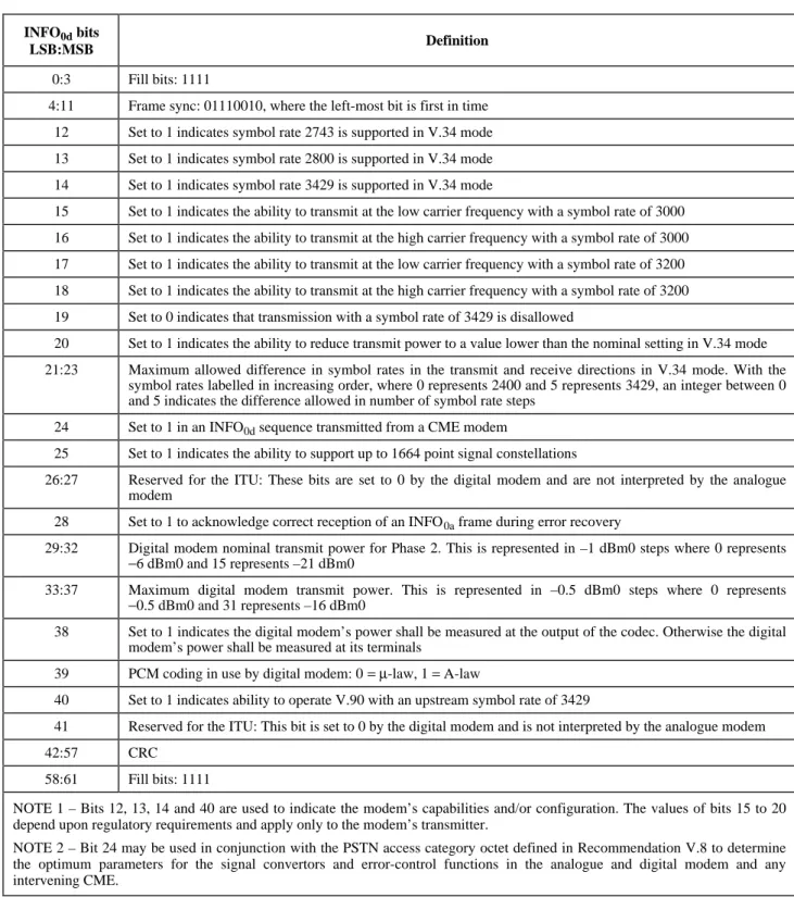
Table 7 defines the bits in the INFO0d sequence. Bit 0 is transmitted first in time.
Table 7/V.90 – Definition of bits in INFO0d
INFO0d bits
LSB:MSB Definition
0:3 Fill bits: 1111
4:11 Frame sync: 01110010, where the left-most bit is first in time 12 Set to 1 indicates symbol rate 2743 is supported in V.34 mode 13 Set to 1 indicates symbol rate 2800 is supported in V.34 mode 14 Set to 1 indicates symbol rate 3429 is supported in V.34 mode
15 Set to 1 indicates the ability to transmit at the low carrier frequency with a symbol rate of 3000 16 Set to 1 indicates the ability to transmit at the high carrier frequency with a symbol rate of 3000 17 Set to 1 indicates the ability to transmit at the low carrier frequency with a symbol rate of 3200 18 Set to 1 indicates the ability to transmit at the high carrier frequency with a symbol rate of 3200 19 Set to 0 indicates that transmission with a symbol rate of 3429 is disallowed
20 Set to 1 indicates the ability to reduce transmit power to a value lower than the nominal setting in V.34 mode 21:23 Maximum allowed difference in symbol rates in the transmit and receive directions in V.34 mode. With the
symbol rates labelled in increasing order, where 0 represents 2400 and 5 represents 3429, an integer between 0 and 5 indicates the difference allowed in number of symbol rate steps
24 Set to 1 in an INFO0d sequence transmitted from a CME modem
25 Set to 1 indicates the ability to support up to 1664 point signal constellations
26:27 Reserved for the ITU: These bits are set to 0 by the digital modem and are not interpreted by the analogue modem
28 Set to 1 to acknowledge correct reception of an INFO0a frame during error recovery
29:32 Digital modem nominal transmit power for Phase 2. This is represented in –1 dBm0 steps where 0 represents
−6 dBm0 and 15 represents –21 dBm0
33:37 Maximum digital modem transmit power. This is represented in –0.5 dBm0 steps where 0 represents
−0.5 dBm0 and 31 represents –16 dBm0
38 Set to 1 indicates the digital modem’s power shall be measured at the output of the codec. Otherwise the digital modem’s power shall be measured at its terminals
39 PCM coding in use by digital modem: 0 =µ-law, 1 = A-law
40 Set to 1 indicates ability to operate V.90 with an upstream symbol rate of 3429
41 Reserved for the ITU: This bit is set to 0 by the digital modem and is not interpreted by the analogue modem
42:57 CRC
58:61 Fill bits: 1111
NOTE 1 – Bits 12, 13, 14 and 40 are used to indicate the modem’s capabilities and/or configuration. The values of bits 15 to 20 depend upon regulatory requirements and apply only to the modem’s transmitter.
NOTE 2 – Bit 24 may be used in conjunction with the PSTN access category octet defined in Recommendation V.8 to determine the optimum parameters for the signal convertors and error-control functions in the analogue and digital modem and any intervening CME.
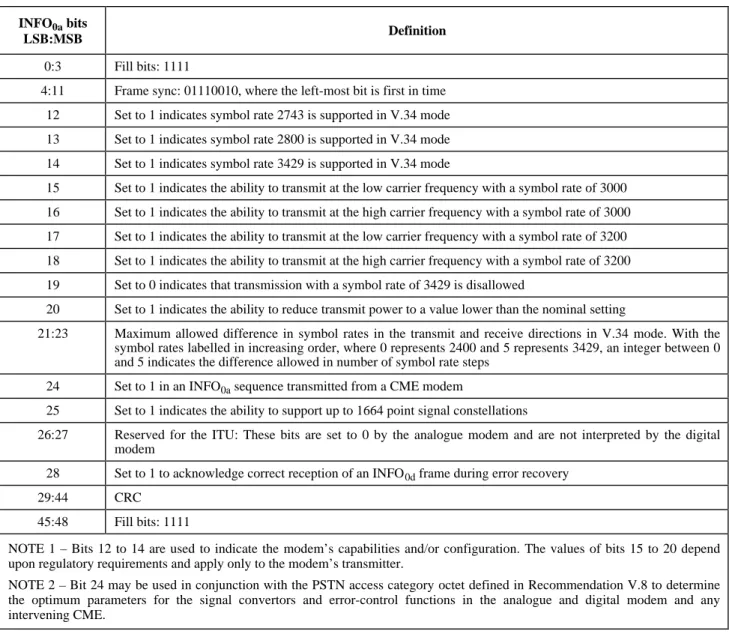
Table 8 defines the bits in the INFO0a sequence. Bit 0 is transmitted first in time.
Table 8/V.90 – Definition of bits in INFO0a
INFO0a bits
LSB:MSB Definition
0:3 Fill bits: 1111
4:11 Frame sync: 01110010, where the left-most bit is first in time 12 Set to 1 indicates symbol rate 2743 is supported in V.34 mode 13 Set to 1 indicates symbol rate 2800 is supported in V.34 mode 14 Set to 1 indicates symbol rate 3429 is supported in V.34 mode
15 Set to 1 indicates the ability to transmit at the low carrier frequency with a symbol rate of 3000 16 Set to 1 indicates the ability to transmit at the high carrier frequency with a symbol rate of 3000 17 Set to 1 indicates the ability to transmit at the low carrier frequency with a symbol rate of 3200 18 Set to 1 indicates the ability to transmit at the high carrier frequency with a symbol rate of 3200 19 Set to 0 indicates that transmission with a symbol rate of 3429 is disallowed
20 Set to 1 indicates the ability to reduce transmit power to a value lower than the nominal setting
21:23 Maximum allowed difference in symbol rates in the transmit and receive directions in V.34 mode. With the symbol rates labelled in increasing order, where 0 represents 2400 and 5 represents 3429, an integer between 0 and 5 indicates the difference allowed in number of symbol rate steps
24 Set to 1 in an INFO0a sequence transmitted from a CME modem
25 Set to 1 indicates the ability to support up to 1664 point signal constellations
26:27 Reserved for the ITU: These bits are set to 0 by the analogue modem and are not interpreted by the digital modem
28 Set to 1 to acknowledge correct reception of an INFO0d frame during error recovery
29:44 CRC
45:48 Fill bits: 1111
NOTE 1 – Bits 12 to 14 are used to indicate the modem’s capabilities and/or configuration. The values of bits 15 to 20 depend upon regulatory requirements and apply only to the modem’s transmitter.
NOTE 2 – Bit 24 may be used in conjunction with the PSTN access category octet defined in Recommendation V.8 to determine the optimum parameters for the signal convertors and error-control functions in the analogue and digital modem and any intervening CME.
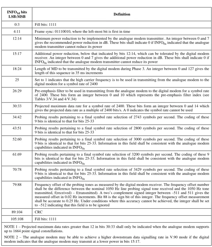
Table 9 defines the bits in the INFO1d sequence. The bit definitions are identical to those of INFO1c in
Recommenda-tion V.34 and are given here for convenience. Bit 0 is transmitted first in time.
Table 9/V.90 – Definition of bits in INFO1d
INFO1d bits
LSB:MSB Definition
0:3 Fill bits: 1111
4:11 Frame sync: 01110010, where the left-most bit is first in time
12:14 Minimum power reduction to be implemented by the analogue modem transmitter. An integer between 0 and 7 gives the recommended power reduction in dB. These bits shall indicate 0 if INFO0a indicated that the analogue
modem transmitter cannot reduce its power
15:17 Additional power reduction, below that indicated by bits 12:14, which can be tolerated by the digital modem receiver. An integer between 0 and 7 gives the additional power reduction in dB. These bits shall indicate 0 if INFO0a indicated that the analogue modem transmitter cannot reduce its power
18:24 Length of MD to be transmitted by the digital modem during Phase 3. An integer between 0 and 127 gives the length of this sequence in 35 ms increments
25 Set to 1 indicates that the high carrier frequency is to be used in transmitting from the analogue modem to the digital modem for a symbol rate of 2400
26:29 Pre-emphasis filter to be used in transmitting from the analogue modem to the digital modem for a symbol rate of 2400. These bits form an integer between 0 and 10 which represents the pre-emphasis filter index (see Tables 3/V.34 and 4/V.34)
30:33 Projected maximum data rate for a symbol rate of 2400. These bits form an integer between 0 and 14 which gives the projected data rate as a multiple of 2400 bits/s. A 0 indicates the symbol rate cannot be used
34:42 Probing results pertaining to a final symbol rate selection of 2743 symbols per second. The coding of these 9 bits is identical to that for bits 25-33
43:51 Probing results pertaining to a final symbol rate selection of 2800 symbols per second. The coding of these 9 bits is identical to that for bits 25-33
52:60 Probing results pertaining to a final symbol rate selection of 3000 symbols per second. The coding of these 9 bits is identical to that for bits 25-33. Information in this field shall be consistent with the analogue modem capabilities indicated in INFO0a
61:69 Probing results pertaining to a final symbol rate selection of 3200 symbols per second. The coding of these 9 bits is identical to that for bits 25-33. Information in this field shall be consistent with the analogue modem capabilities indicated in INFO0a
70:78 Probing results pertaining to a final symbol rate selection of 3429 symbols per second. The coding of these 9 bits is identical to that for bits 25-33. Information in this field shall be consistent with the analogue modem capabilities indicated in INFO0a
79:88 Frequency offset of the probing tones as measured by the digital modem receiver. The frequency offset number shall be the difference between the nominal 1050 Hz line probing signal tone received and the 1050 Hz tone transmitted, f(received) – f(transmitted). A two’s complement signed integer between –511 and 511 gives the measured offset in 0.02 Hz increments. Bit 88 is the sign bit of this integer. The frequency offset measurement shall be accurate to 0.25 Hz. Under conditions where this accuracy cannot be achieved, the integer shall be set to –512 indicating that this field is to be ignored
89:104 CRC
105:108 Fill bits: 1111
NOTE 1 – Projected maximum data rates greater than 12 in bits 30:33 shall only be indicated when the analogue modem supports up to 1664 point signal constellations.
NOTE 2 – The analogue modem may be able to achieve a higher downstream data signalling rate in V.90 mode if the digital modem indicates that the analogue modem may transmit at a lower power in bits 15:17.
Table 10 defines the bits in the INFO1a sequence that an analogue modem uses to request Phase 3 of this
Recommendation. Bits 37:39 represent the integer 6, indicating that V.90 operation is desired. Bit 0 is transmitted first in time.
Table 10/V.90 – Definition of bits in INFO1a when V.90 is selected
Table 11 defines the bits in the INFO1a sequence that an analogue modem uses to request Phase 3 of
Recommen-dation V.34. The bit definitions are identical to those of INFO1a in Recommendation V.34 and are given here for
convenience. Bits 37:39 represent an integer between 0 and 5, indicating that V.34 operation is desired. Bit 0 is transmitted first in time.
8.2.3.3 INFOMARKS
INFOMARKSd is created by the digital modem applying binary ones to the DPSK modulator described in 8.2.3.1.
INFOMARKSa is created by the analogue modem applying binary ones to the DPSK modulator described in 8.2.3.1.
8.2.4 Line probing signals
As defined in 10.1.2.4/V.34.
8.3 Phase 3 signals for the analogue modem
The analogue modem shall use the polynomial, GPA, in equation 7-2/V.34 when generating signals Ja, TRN and SCR.
INFO1a bits
LSB:MSB Definition
0:3 Fill bits: 1111
4:11 Frame sync: 01110010, where the left-most bit is first in time
12:17 Reserved for the ITU: These bits are set to 0 by the analogue modem and are not interpreted by the digital modem
18:24 Length of MD to be transmitted by the analogue modem during Phase 3. An integer between 0 and 127 gives the length of this sequence in 35 ms increments
25:31 UINFO: Ucode of the PCM codeword to be used by the digital modem for the 2 point train. The power of this
point shall not exceed the maximum digital modem transmit power. UINFO shall be greater than 66
32:33 Reserved for the ITU: These bits are set to 0 by the analogue modem and are not interpreted by the digital modem
34:36 Symbol rate to be used in transmitting from the analogue modem to the digital modem. An integer between 3 and 5 gives the symbol rate, where 3 represents 3000 and 5 represents 3429. The symbol rate selected shall be consistent with information in INFO1d. The carrier frequency and pre-emphasis filter to be used are those
already indicated for this symbol rate in INFO1d
37:39 Symbol rate of 8000 to be used by the digital modem: The integer 6
40:49 Frequency offset of the probing tones as measured by the analogue modem receiver. The frequency offset number shall be the difference between the nominal 1050 Hz line probing signal tone received and the 1050 Hz tone transmitted, f(received) – f(transmitted). A two’s complement signed integer between –511 and 511 gives the measured offset in 0.02 Hz increments. Bit 9 is the sign bit of this integer. The frequency offset measurement shall be accurate to 0.25 Hz. Under conditions where this accuracy cannot be achieved, the integer shall be set to –512 indicating that this field is to be ignored
50:65 CRC
Table 11/V.90 – Definition of bits in INFO1a when V.34 is selected
8.3.1 Ja
Sequence Ja consists of repetitions of the DIL descriptor detailed below. The modulation used for transmitting Ja is as
defined in 10.1.3.3/V.34. Transmission of sequence Ja may be terminated without completing the final DIL descriptor.
The DIL descriptor tells the digital modem what parameters to use when transmitting DIL. The bit fields in the DIL descriptor are given in Table 12. Definitions and interpretation of the parameters are given in 8.4.1. Due to the variability in the length of the sequences SP and TP the bit numbers are given using α = (LSP)/16*17 and β = α
+ (LTP)/16*17, where x is the smallest integer higher than or equal to x. When LSP is not a multiple of 16, zeroes
shall be used to pad SP to the next multiple of 16 bits so that the format of the Ja sequence is preserved. Similarly, when
LTP is not a multiple of 16, zeroes shall be used to pad TP to the next multiple of 16 bits. LSP – 1 = LTP – 1 = 0 when
N = 0. The values for SP and TP have no significance when N = 0.
The CRC generator used is described in 10.1.2.3.2/V.34. INFO1a bits
LSB:MSB Definition
0:3 Fill bits: 1111
4:11 Frame sync: 01110010, where the left-most bit is first in time
12:14 Minimum power reduction to be implemented by the digital modem transmitter. An integer between 0 and 7 gives the recommended power reduction in dB. These bits shall indicate 0 if INFO0d indicated that the digital
modem transmitter cannot reduce its power
15:17 Additional power reduction, below that indicated by bits 12:14, which can be tolerated by the analogue modem receiver. An integer between 0 and 7 gives the additional power reduction in dB. These bits shall indicate 0 if INFO0d indicated that the digital modem transmitter cannot reduce its power
18:24 Length of MD to be transmitted by the analogue modem during Phase 3. An integer between 0 and 127 gives the length of this sequence in 35 ms increments
25 Set to 1 indicates that the high carrier frequency is to be used in transmitting from the digital modem to the analogue modem. This shall be consistent with the capabilities of the digital modem indicated in INFO0d
26:29 Pre-emphasis filter to be used in transmitting from the digital modem to the analogue modem. These bits form an integer between 0 and 10 which represents the pre-emphasis filter index (see Tables 3/V.34 and 4/V.34) 30:33 Projected maximum data rate for the selected symbol rate from the digital modem to the analogue modem.
These bits form an integer between 0 and 14 which gives the projected data rate as a multiple of 2400 bits/s 34:36 Symbol rate to be used in transmitting from the analogue modem to the digital modem. An integer between 0
and 5 gives the symbol rate, where 0 represents 2400 and a 5 represents 3429. The symbol rate selected shall be consistent with information in INFO1d and consistent with the symbol rate asymmetry allowed as indicated in
INFO0a and INFO0d. The carrier frequency and pre-emphasis filter to be used are those already indicated for
this symbol rate in INFO1d
37:39 Symbol rate to be used in transmitting from the digital modem to the analogue modem. An integer between 0 and 5 gives the symbol rate, where 0 represents 2400 and a 5 represents 3429. The symbol rate selected shall be consistent with the capabilities indicated in INFO0a and consistent with the symbol rate asymmetry allowed as
indicated in INFO0a and INFO0d
40:49 Frequency offset of the probing tones as measured by the analogue modem receiver. The frequency offset number shall be the difference between the nominal 1050 Hz line probing signal tone received and the 1050 Hz tone transmitted, f(received) – f(transmitted). A two’s complement signed integer between –511 and 511 gives the measured offset in 0.02 Hz increments. Bit 49 is the sign bit of this integer. The frequency offset measurement shall be accurate to 0.25 Hz. Under conditions where this accuracy cannot be achieved, the integer shall be set to –512 indicating that this field is to be ignored
50:65 CRC
66:69 Fill bits: 1111
NOTE – Projected maximum data rates greater than 12 in bits 30:33 shall only be indicated when the digital modem supports up to 1664 point signal constellations.
Table 12/V.90 – Definition of bits in the DIL descriptor
LSB:MSB Definition
0:16 Frame sync: 11111111111111111 17 Start bit: 0
18:25 N
26:33 Reserved for ITU: These bits are set to 0 by the analogue modem and are not interpreted by the digital modem
34 Start bit: 0 35:41 LSP – 1
42 Reserved for ITU: This bit is set to 0 by the analogue modem and is not interpreted by the digital modem 43:49 LTP – 1
50 Reserved for ITU: This bit is set to 0 by the analogue modem and is not interpreted by the digital modem 51 Start bit: 0
52:67 SP
68 Start bit: 0
Possible continuation of SP with a start bit (0) every 16 bits 51+α Start bit: 0
52+α:67+α TP 68+α Start bit: 0
Possible continuation of TP with a start bit (0) every 16 bits 51+β Start bit: 0
52+β:58+β H1
59+β Reserved for ITU: This bit is set to 0 by the analogue modem and is not interpreted by the digital modem 60+β:66+β H2
67+β Reserved for ITU: This bit is set to 0 by the analogue modem and is not interpreted by the digital modem 68+β Start bit: 0
69+β:75+β H3
76+β Reserved for ITU: This bit is set to 0 by the analogue modem and is not interpreted by the digital modem 77+β:83+β H4
84+β Reserved for ITU: This bit is set to 0 by the analogue modem and is not interpreted by the digital modem 85+β Start bit: 0
86+β:92+β H5
93+β Reserved for ITU: This bit is set to 0 by the analogue modem and is not interpreted by the digital modem 94+β:100+β H6
101+β Reserved for ITU: This bit is set to 0 by the analogue modem and is not interpreted by the digital modem 102+β Start bit: 0
103+β:109+β H7
Table 12/V.90 – Definition of bits in the DIL descriptor (concluded)
LSB:MSB Definition
111+β:117+β H8
118+β Reserved for ITU: This bit is set to 0 by the analogue modem and is not interpreted by the digital modem 119+β Start bit: 0
120+β:126+β REF1
127+β Reserved for ITU: This bit is set to 0 by the analogue modem and is not interpreted by the digital modem 128+β:134+β REF2
135+β Reserved for ITU: This bit is set to 0 by the analogue modem and is not interpreted by the digital modem 136+β Start bit: 0
137+β:143+β REF3
144+β Reserved for ITU: This bit is set to 0 by the analogue modem and is not interpreted by the digital modem 145+β:151+β REF4
152+β Reserved for ITU: This bit is set to 0 by the analogue modem and is not interpreted by the digital modem 153+β Start bit: 0
154+β:160+β REF5
161+β Reserved for ITU: This bit is set to 0 by the analogue modem and is not interpreted by the digital modem 162+β:168+β REF6
169+β Reserved for ITU: This bit is set to 0 by the analogue modem and is not interpreted by the digital modem 170+β Start bit: 0
171+β:177+β REF7
178+β Reserved for ITU: This bit is set to 0 by the analogue modem and is not interpreted by the digital modem 179+β:185+β REF8
186+β Reserved for ITU: This bit is set to 0 by the analogue modem and is not interpreted by the digital modem 187+β Start bit: 0
188+β:194+β The Ucode of the training symbol used for the 1st DIL segment
195+β Reserved for ITU: This bit is set to 0 by the analogue modem and is not interpreted by the digital modem 196+β:202+β The Ucode of the training symbol used for the 2nd DIL segment
203+β Reserved for ITU: This bit is set to 0 by the analogue modem and is not interpreted by the digital modem 204+β Start bit: 0
Remaining Ucodes of training symbols with a start bit (0) every 16 bits and appropriate reserved bits including 9 reserved bits to fill the final 16 bits if N is odd
187+β+N/2*17 Start bit: 0 188+β+N/2*17:
203+β+N/2*17
CRC
204+β+N/2*17 Fill bit: 0
NOTE – It is highly desirable that the analogue modem requests a DIL that does not allow echo control devices in the switched digital network to re-enable. The analogue modem may also continuously transmit SCR during the reception of DIL to maintain line energy.
8.3.2 MD As defined in 10.1.3.5/V.34. 8.3.3 PP As defined in 10.1.3.6/V.34. 8.3.4 S As defined in 10.1.3.7/V.34. 8.3.5 SCR
Signal SCR is defined as binary ones modulated according to 10.1.3.9/V.34 except that neither the scrambler nor the differential encoder need be initialized at the beginning of its transmission. During Phase 3 and Phase 4 start-up procedures the constellation size depends on bit 47 of Jd. During rate renegotiation procedures the constellation size
depends on bit 48 of Jd.
8.3.6 TRN
As defined in 10.1.3.8/V.34 using a 4-point 2D constellation.
8.4 Phase 3 signals for the digital modem
The digital modem shall use the polynomial, GPC, in equation 7-1/V.34 when generating signals Jd, Jd′ and TRN1d.
Signals transmitted by the digital modem during Phase 3 are not spectrally shaped.
8.4.1 DIL
The parameters necessary for the digital modem to form the DIL are sent to it by the analogue modem using the DIL descriptor defined in 8.3.1.
The DIL consists of N DIL-segments of length Lc where:
0 ≤ N ≤ 255;
1 ≤ c ≤ 8; and
Lc = (Hc + 1) * 6 symbols.
Eight Hc values are used to calculate the length of the DIL-segments containing training symbols from each Uchord.
H1 shall be used to calculate the length of the DIL-segments containing training symbols from Uchord1, H8 shall be used
to calculate the length of the DIL-segments containing training symbols from Uchord8.
Eight Ucodes, REFc, define the PCM codeword used as a reference symbol in DIL-segments containing training
symbols from each Uchord. The PCM codeword given by the Ucode REF1 shall be used as a reference symbol in
DIL-segments containing training symbols from Uchord1, the PCM codeword given by the Ucode REF8 shall be used as
a reference symbol in DIL-segments containing training symbols from Uchord8.
A single Sign Pattern (SP) and Training Pattern (TP) is used for the entire DIL. An SP bit determines the sign of a transmitted symbol. 0 shall represent negative and 1 shall represent positive. A TP bit determines whether the reference symbol (REFc) or a training symbol is transmitted. 0 shall represent REFc and 1 shall represent a training symbol. The
LSB of each pattern applies to the first symbol of a DIL-segment. The lengths of these patterns are: 1 ≤ LSP ≤ 128; and
The patterns are restarted at the beginning of each DIL-segment. The patterns are repeated independently within DIL-segments whose lengths exceed that of LSP or LTP.
The entire sequence, not just the last DIL-segment, is repeated until either the analogue modem causes it to be terminated or a timeout occurs. The sequence shall be terminated on a DIL-segment boundary.
A set of N Ucodes determine the training symbol that is assigned to each DIL-segment. The first of the N Ucodes specifies the training symbol assigned to the first DIL-segment and so on.
When N = 0, DIL is not transmitted.
8.4.2 Jd
Sequence Jd consists of a whole number of repetitions of the bit pattern given in Table 13. Bit 0 is transmitted first. The
bits are scrambled and differentially encoded and then transmitted as the sign of the PCM codeword whose Ucode is UINFO. A sign of 0 represents a negative voltage, a sign of 1 represents a positive voltage. The differential encoder
shall be initialized with the final symbol of the transmitted TRN1d.
The CRC generator used is described in 10.1.2.3.2/V.34.
Table 13/V.90 – Definition of bits in Jd
8.4.3 Jd′
′
Jd is used to terminate Jd. Jd′ consists of 12 binary zeroes. The bits are scrambled and differentially encoded and then transmitted as the sign of the PCM codeword whose Ucode is UINFO. A sign of 0 represents a negative voltage, a sign of
1 represents a positive voltage. The differential encoder shall be initialized with the final symbol of the transmitted Jd.
8.4.4 Sd
Sd consists of 64 repetitions of the sequence {+W, +0, +W, –W, –0, –W} where W is defined to be the PCM codeword
whose Ucode is 16 + UINFO and 0 is the PCM codeword with Ucode 0. Sd consists of 8 repetitions of the sequence
{−W, –0, –W, +W, +0, +W}.
The first symbol of Sd is defined to be transmitted in data frame interval 0. The digital modem shall keep data frame alignment from this point on.
Jd bits
LSB:MSB Definition
0:16 Frame Sync: 11111111111111111 17 Start bit: 0
18:33 Data signalling rate capability mask.
Bit 18:28 000; bit 19:29 333; bit 20:30 666; …; bit 33:48 000. Bits set to 1 indicate data signalling rates supported and enabled in the transmitter of the digital modem
34 Start bit: 0
35:46 Data signalling rate capability mask (contd.).
Bit 35:49 333; bit 36:50 666; …; bit 39:54 666; bit 40:56 000; bits 41 to 46: Reserved for ITU. (These bits are set to 0 by the digital modem and are not interpreted by the analogue modem.) Bits set to 1 indicate data signalling rates supported and enabled in the transmitter of the digital modem
47 Size of constellation used to transmit CP, E and SCR during training sequences: 0 = 4-point constellation; 1 = 16-point constellation
48 Size of constellation used to transmit CP, E and SCR during rate renegotiation procedures: 0 = 4-point constellation; 1 = 16-point constellation
49:50 A number between 1 and 3 indicating the digital modem’s maximum lookahead for spectral shaping 51 Start bit: 0
52:67 CRC
8.4.5 TRN1d
Signal TRN1d is a sequence of the PCM codeword whose Ucode is UINFO with signs generated by applying binary ones
to the input of the scrambler described in 5.3. A sign of 0 represents a negative voltage, a sign of 1 represents a positive voltage. The scrambler is initialized to zero prior to the transmission of TRN1d. TRN1d shall be an integer multiple of
6 symbols long.
8.5 Phase 4 signals for the analogue modem
8.5.1 B1
As defined in 10.1.3.1/V.34.
8.5.2 CP
CP sequences consist of symbols chosen from a 4- or 16-point 2D constellation. During Phase 4 start-up procedures the constellation size depends on bit 47 of Jd. During rate renegotiation procedures the constellation size depends on bit 48 of Jd. CP is used by the analogue modem to pass constellation parameters to the digital modem. A CPt sequence is sent
to pass the parameters used by the digital modem in Phase 4 training. A CP sequence with the acknowledge bit set to 1 is denoted by CP′. A CP sequence with the request for silence bit set is denoted CPs. Due to the nature of the procedures
that use CPs, the constellation parameters contained in CPs are not used. The average power of the constellations that the
analogue modem requests the digital modem to use during data mode shall not be greater than 3 dB above the average power of the constellations it requests the digital modem to use during Phase 4.
CP sequences are modulated according to 10.1.3.9/V.34. The scrambler and differential encoder are initialized to zero prior to the transmission of the first CPt sequence. Bit fields for CP sequences are defined in Table 14. Bit 0 is
transmitted first.
The CRC generator used is described in 10.1.2.3.2/V.34.
CP sequences are defined to be of variable length. A constellation mask consists of 128 bits where a bit set to 1 indicates that the constellation includes the PCM code represented by the corresponding Ucode. Only the number of different constellations need to be sent. The constellations that are sent are indexed from 0 (in bits 136:271) to a maximum of 5 (in bits 816:951). If the constellations at the digital modem’s transmitter differ from those at the output to the codec’s D/A convertor, then bit 128 shall be set and the constellation at the output to the codec’s D/A convertor corresponding to each transmit constellation shall be sent. Due to the variability in the number of constellations, a parameter γ is defined to be 136* (the maximum constellation index given in bits 103:127) and a parameter δ is defined to be (2*γ)+136 if bit 128 is set and γ if bit 128 is clear.
When multiple CP and CP′ sequences are transmitted as a group, they shall all contain identical modulation and spectral shaping parameter information.
Table 14/V.90 – Definition of bits in CP
CP bits
LSB:MSB Definition
0:16 Frame Sync: 11111111111111111 17 Start bit: 0
18 Reserved for ITU: This bit is set to 0 by the analogue modem and is not interpreted by the digital modem 19 0 indicates CPt; 1 indicates CP
20:24 Selected digital modem to analogue modem data signalling rate, an integer, drn, between 0 and 22. drn = 0 indicates cleardown.
Data signalling rate = (drn+20)*8000/6 in CP and (drn+8)*8000/6 in CPt.
25:29 Reserved for ITU: These bits are set to 0 by the analogue modem and are not interpreted by the digital modem
30 Set to 1 indicates a silent period is requested. This may be used during rate renegotiation (see 9.6) 31:32 Sr: The number of sign bits used as redundancy for spectral shaping
33 Acknowledge bit: 0 = modem has not received MP from far end; 1 = received MP from far end 34 Start bit: 0
35 Codec type: 0 =µ-law; 1 = A-law
36:48 Analogue modem to digital modem data signalling rate capability mask:
Bit 36:4800; …; bit 47:31 200; bit 48:33 600. Bits set to 1 indicate data signalling rates supported and enabled in analogue modem transmitter
49:50 ld: Number of look-ahead frames requested during spectral shaping. This shall be consistent with the capabilities of the digital modem indicated in Jd
51 Start bit: 0
52:67 The RMS value of TRN1d at the transmitter output divided by the RMS value of TRN1d at the output to the
codec’s D/A convertor expressed in unsigned Q3.13 format (xxx.xxxxxxxxxxxxx) 68 Start bit: 0
69:76 Parameter a1 of the spectral shaping filter in signed Q1.6 format (sx.xxxxxx)
77:84 Parameter a2 of the spectral shaping filter in signed Q1.6 format (sx.xxxxxx)
85 Start bit: 0
86:93 Parameter b1 of the spectral shaping filter in signed Q1.6 format (sx.xxxxxx)
94:101 Parameter b2 of the spectral shaping filter in signed Q1.6 format (sx.xxxxxx)
102 Start bit: 0
103:106 An integer between 0 and 5 denoting the index of the constellation to be used in data frame interval 0 107:110 An integer between 0 and 5 denoting the index of the constellation to be used in data frame interval 1 111:114 An integer between 0 and 5 denoting the index of the constellation to be used in data frame interval 2 115:118 An integer between 0 and 5 denoting the index of the constellation to be used in data frame interval 3
119 Start bit: 0
120:123 An integer between 0 and 5 denoting the index of the constellation to be used in data frame interval 4 124:127 An integer between 0 and 5 denoting the index of the constellation to be used in data frame interval 5
![Figure I.1/V.90 – Example network configuration FIGURE I.1/V.90...[D11] = 3 CM](https://thumb-us.123doks.com/thumbv2/123dok_us/9594060.2837242/49.892.85.815.990.1102/figure-i-v-example-network-configuration-figure-cm.webp)
