R E S E A R C H
Open Access
An inter-FPGA communication bus with
error detection and dynamic clock phase
adjustment
LT Melo
1*†, SHC Santana
1, AG Silva-Filho
1†, ME Lima
1, VWC Medeiros
2†and MLM Marinho
2Abstract
Background: Nowadays, systems involving multiple FPGAs are used for various scientific applications. Such systems require a data bus dedicated to the communication between FPGAs, which could be done through a LVDS type. Another important factor is that the routing that interconnects the LVDS pins on the platform should be precisely developed to avoid instabilities in communication. Unfortunately, many platforms available in the market do not observe such restrictions, limiting the throughput of the bus.
Methods: This paper presents an inter-FPGAs communication channel based on a DDR interface directed to this kind of platform. This approach promotes a stable communication between these devices without the use of LVDS pins. An error detection module was also designed to ensure the sending integrity and correct any errors on the bus. A mechanism for dynamic and automatic clock phase adjustment used on the bus was also implemented to ensure that the developed modules were compatible with other platforms.
Results: The channel has been implemented in a PROCStarIII platform and rates of 4.76 Gbps were achieved. Conclusions: The channel has been validated on a commercial platform with success and the synthesis results, as well as the performance results obtained by using it in a real implementation of the RTM algorithm, are also presented.
Keywords: LVDS; FPGA; CRC; Communication inter-FPGAs
Background
Platforms that involve multiple field-programmable gate arrays (FPGAs) have been the target of several study fields such as prototyping of MPSoCs (multiprocessor system-on-chip), acceleration, and encryption algorithms [1, 2]. For these systems to work efficiently using exist-ing resources in FPGAs, an efficient communication must exist between the FPGAs available on the platform. This type of communication in next-generation FPGAs is usu-ally established through type interfaces low-voltage differ-ential signaling (LVDS) [3]. This type of signaling allows signal sending at high speed through a differential pair of parallel wire. The use of this feature enables data
*Correspondence: [email protected]
†Equal contributor
1Center for Informatics, Federal University of Pernambuco, Av. Jornalista Anibal Fernandes, s/n Cidade Universitaria, 50.740-560 Recife, Brazil Full list of author information is available at the end of the article
transmission between devices to be performed more effi-ciently, allowing a more secure communication when fac-ing electromagnetic interference [4, 5]. This configuration enables busses to achieve transfer rates of about 10 Gbps by using more advanced devices such as the Xilinx Virtex [6] family of FPGAs, Altera Stratix V [7] FPGAs.
Currently, many FPGAs support LVDS interfaces, and by being properly allocated on the platform, they can pro-vide data communication at a high transmission rate by using their transceivers. However, some platforms avail-able in the market were not designed to accommodate the LVDS FPGA pin resources in their communication lines, thus preventing the LVDS transceiver use and there-fore hindering the implementation of communication channels with high performance. Other factors such as distance between tracks, resistance, and capacitance bal-ance are important and need to be observed by this type
of platform manufacturers. Data transmission performed without these resources can lead to errors in data transfer when the transmission rate is high, as there is no guar-antee that data integrity is maintained. This is because of all FPGA I/O (Input/Output) pins that are generally subject to physical interference. Due to this possible low performance in data transmission, systems using these resources will have to reduce their logic module speed to suit the channel and thereby reduce the incidence of communication error.
This paper presents a bi-directional synchronized com-munication channel (full-duplex) regardless of LVDS interface use. To ensure a good transmission rate of the transmitter, it is based on a double data rate (DDR) inter-face, and to ensure data integrity, detection modules based on the generation and error checking cyclic redundancy check (CRC) were developed. Additionally, a module to fit automatically and dynamically the clock phase of the communication bus was also created. An example using the bus for reverse time migration (RTM) processing algorithm in a multi-FPGA platform is also presented.
After the introduction section, this paper is structured as follows: The section “Related work” discusses the work related to this article. In the section “GiDEL PROCStarIII platform”, the platform used in the experiments is shown. In the section “Methods”, the developed architecture is presented. In the section “Results”, the results of the experiments are shown. Finally, the section “Conclusions” contains the conclusion of this work.
Related work
In this section, some studies focusing on inter-FPGA communication are presented. The paper [8] presents an architecture for this purpose, and the work [9] proposes a solution for optimizing communication between different FPGA devices.
The work [8] presents an architecture for inter-FPGA full-duplex communication with 18 LVDS transmission tracks. The architecture is based on DDR interface and consists of a transmitter and a receiver. The authors demonstrate that it is possible to reach transfer rates of about 10 Gbps by using this approach. The architecture is designed to be implemented in a high-performance cluster (PARAMNet-3) [10]. The architecture comprises a network switch allowing package routing to be performed at high speed. Each board being part of the switch con-sists of four FPGAs from Xilinx Virtex-4 and transceivers (multi-gigabit transceivers) available inside each FPGA. These transceivers are used for communication with the other system boards.
The transmitter consists of a control unit, LVDS I/O buffers, and a serializer/deserializer (SERDES) module. These last two features are I/O already available in the Xilinx Virtex-4 FPGA. The SERDES module is a
serializer/deserializer that receives the application data in parallel and serializes it. The LVDS output buffers receive this serialized data and implement the output to 18 tracks of differential pairs. Each track has a transfer rate of 625 Mbps, summing up a total rate of about 10 Gbps.
The receiver has its clock generated by the transmitter. This allows synchronization of both sides. It consists of a control module, delays, SERDES I/O buffers, and LVDS module. The delay modules are responsible for introduc-ing a 5–10 ps jitter on the clock input from the transmitter. This strategy respects the valid data window and is nec-essary to ensure that signals are received in the receiver correctly. The clock used in the receiver is of 312.5 MHz and is synchronized with the transmitter.
Communication error detection is performed on the network layer of the switch, and the authors have devel-oped a test engine to generate errors in the communica-tion channel. This engine is responsible for testing each LVDS track, and two instances were implemented in each FPGA. The testing environment consists of a PowerPC processor executing an application that communicates with the architecture via a UART interface. It can be con-figured with test parameters and statistics view on the application.
In [9], a solution for optimizing inter-FPGA commu-nication using channel adaptation is shown. The work demonstrates that each platform has its own characteris-tics, and to migrate up the project to another platform, you often need to change the architecture to adapt to necessary changes. The communication bus width, point-to-point broadcast, or LVDS are some of the options that could be parameterized by abstracting from the users that need to change theirs. In that sense, the authors of the work propose a definable channel and one that is able to self-adapt the target architecture.
Initially, it seems to be an architecture that consists of a base control module, FIFOs (First In, First Out), and PHY modules transmit (TX) and receive (RX). The architecture supports SDR/DDR interfaces and point-to-point trans-mission or LVDS. It can therefore be used for SERDES modules, serialization/deserialization of data, and it can be defined whether the communication is unidirectional or bidirectional. Finally, the architecture allows the bus width to be configurable.
The channel adaptation, called chAdapt, consists of a hardware module that self-configures the transmission according to the platform characteristics. For this, a trans-mission of a bit sequence occurs repeatedly between the transmitter and receiver, initially to identify possible delays in the communication form. At that time, all the controls are optimized and clock alignment is performed by dynamically adjusting its phase.
platform allows the adaptation of different reconfigurable modules that consist of Xilinx FPGAs. The tests were per-formed with the following FPGAs: Spartan-3A, Spartan-6, Virtex-4, and Virtex-5. Several combinations were ana-lyzed in order to find possible optimizations in the communication. As a result, the authors demonstrate a comparative table between combinations used, highlight-ing the relative optimization after the addition of chAdapt module architecture. The tests performed with the com-munication between Virtex-4 and Spartan-6 are notewor-thy. A significant improvement in communication was observed after the introduction of chAdapt in these sce-narios. The results indicate that although it was not pos-sible to align the bus width for these tests, the channel offers a great way when implemented for the communi-cation link validation and identifying best parameters for data transfer.
GiDEL PROCStarIII platform
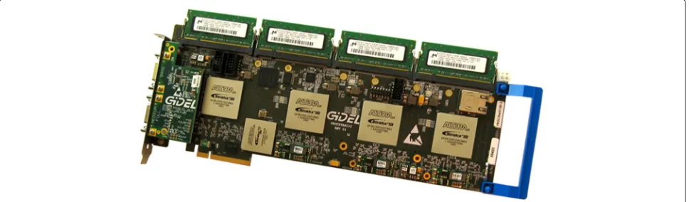
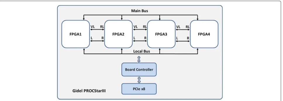
The communication channel presented in this work was implemented in a GiDEL PROCStarIII platform (Fig. 1) [12]. This platform consists of four Altera Stratix III 260E and has three memory banks: one of 512 MB DDR2 mem-ory and two banks composed of 8 DDR2 SODIMMs with up to 4 GB each.
Although the platform has four FPGAs, it is not possi-ble for the inter-FPGA communication to use differential pairs available in these devices. This occurs because the FPGA pins used in the platform, directly connected to the bus, are I/O common pins. Another aspect is that there are no guarantees related to the printed circuit board (PCB) layout of the platform. Characteristics like resis-tance, capaciresis-tance, and bus route length that connect the FPGAs are not guaranteed to obtain a stable communi-cation. For those reasons, the high-speed communication cannot be achieved. The local bus is responsible for con-necting all FPGAs to the host controller through PCIex8. The communication protocol for this bus is automati-cally generated in the ProcWizard [13] tool. The main bus
connects all the FPGAs and has a width of 40 bits. Figure 2 shows the internal architecture of the PROCStarIII plat-form.
For data communication, two busses are available: VL-RL bus and LR bus. Each bus connects the adjacent FPGAs available on the platform. The VL-RL bus has a width of 10 bits and is type I/O common pins. The sig-nals used in this bus have a voltage of 1.8 V. The LR bus has a width of 100 bits and is also type I/O com-mon pins. The LR bus, besides being the largest available, concentrates a single bank of pins that can be used in the communication channel. This minimizes the impact related to data skew since their paths are aligned. Thus, potential signal delay problems are decreased. Due to these characteristics, the proposed architecture in this paper uses the LR bus to implement the communication channel.
The platform also offers JTAG connectors that can be used for debugging and has PSDB connectors (PROC-StarIIIdaughterboards), which are high-speed interfaces used to connect other cards provided by the manufacturer (camera links, ethernet interfaces, etc.).
Methods
The communication system proposed by this work is defined as a parallel communication channel, synchro-nized and 32 bits wide. Each controller is comprised of two main modules: a transmitter and a receiver. A com-mon clock synchronizes the communication in the chan-nel. This system can then be coupled in each FPGA to allow data communication between these devices on the platform.
The entire system was designed to facilitate its adapta-tion to different projects. To make this possible, a FIFO input on the transmitter and a FIFO output on the receiver were used, making the design transparent to the user. The adjustments for each application should be made through few adjustments in the input and output parameters of each FIFO.
Fig. 2GiDEL PROCStarIII platform diagrams. Overview of the platform architecture
Figure 3 shows the communication channel between two FPGAs involving the main signals from the transmit-ter and receiver.
One signal of 33 bits (data_bus) was defined for trans-ferring data between devices. One bit ofdata_bussignal is intended for a valid signal, which indicates to the receiver that the data sent is valid and that it can be received and forwarded to the CRC check module and later to the FIFO output. Thus, the communication channel enables a data transfer with a width of 32 bits between the FPGAs.
The critical clk_bus signal is used to feed the clock signal to the receiver. The clock signal is generated in the transmitter through a PLL (Phase-Locked Loop) and sent to the receiver through a path reserved for this pur-pose. This ensures that both the transmitter and receiver are synchronized allowing the communication channel to operate stably. The synchronization and transmission fail-ure signals that also incorporate the bus will be discussed in the next sections.
Transmitter
The transmission module, called Transmitter, is respon-sible for sending the data correctly through the bus. It is also its responsibility to align the clock with the availabil-ity of data on the bus, thus increasing utilization of the
Fig. 3Main signals from the communication bus. Detailed signalization of the communication bus
data valid window, and to re-transmit the data if an error occurs in transmission. The transmitter also has a module for generating CRC for the data sent. After transmitting a data package, a checksum that validates the package is sent through the bus to be checked at the receiver. If errors are found during the verification, a request for retransmission is performed.
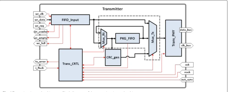
To perform these tasks, the Transmitter module is divided into five modules: a FIFO input (FIFO_INPUT), the retransmission circuit, the CRC generator (CRC_ GEN), the physical layer (TRANS_PHY), and the control transmitter (TRANS_CTRL), as shown in Fig. 4.
The moduleFIFO_INPUT is available in MegaWizard that goes along with the tool development Altera Quartus II. This input module aims to standardize the interface of the transmission module with the architecture in which it is inserted and receive the data to be transferred. Its architecture allows it to work internally with a differ-ent frequency from the transmitter module to which it is coupled. Commonly, its internal frequency is higher than the one used in the system, and thus, the speed of data removal from the FIFO may be greater than the speed at which it is inserted.
For greater flexibility in the transmission process, the data width that will be inserted and FIFO depth are adjustable as needed through the use of configuration parameters of the transmitter. By default, the data width is of 128 bits and the FIFO depth is of 256 words.
Fig. 4Transmitter internal architecture. Block diagrams of the transmitter internal architecture
into FIFO. Thewr_usedwsignal indicates to the internal architecture how many words there are in FIFO. Finally, the wr_empty signal indicates when FIFO is empty and
wr_fullsignal indicates when FIFO is full. All these signals have been made available so that the user can monitor the status of FIFO input and have full control of writing data for transmission.
The communication occurs on the bus through pack-ages. By default, the size of the package to be transferred is of eight words of 32 bits, as the bus only supports this data transmission width. In this case, two words of the input FIFO (256 bits) are required to form a package. Based on this example, the transmitter removes the data from FIFO input and divides it. The first division occurs at the out-put of FIFO inout-put. By default, the outout-put is of 64 bits. The second one is made within theTRANS_PHYmodule that divides each data of 64 bits into two of 32 bits.
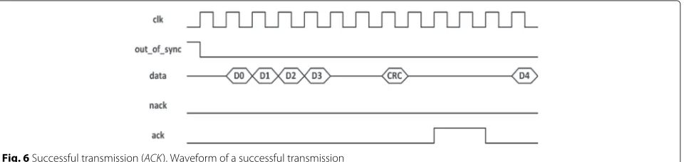
Each data package is sent to the bus, and then a check-sum is immediately sent to verify the integrity of the package at the receiver. If a match is found in the check-sum verification at the receiver, it sends anACK signal to the transmitter indicating that the package has been received successfully; otherwise, a NACK signal is sent and a retransmission occurs.
The retransmission circuit is highlighted in Fig. 4. This circuit is responsible for keeping the data package to be transmitted in its structure and, in case of failure, retrans-mit it in the fastest possible time. Because of that, this circuit has a FIFO (PKG_FIFO), which stores the pack-age to be transmitted, and two multiplexers (MUX_RT
andMUX_TX) that select the correct path for the data to be sent. The data package to be transmitted, after being required in theFIFO_INPUT, goes to the physical layer (TRANS_PHY) through theMUX_TXcomponent. Simultaneously, a copy of the package is temporarily
stored in the retransmission FIFO (PKG_FIFO) by the
MUX_RT component. If there is a problem in the trans-mission, and the NACK signal takes a high logic level, the data previously stored in PKG_FIFO will be read and transmitted to the receiver via the MUX_TX and
TRANS_PHY modules, respectively. A feedback loop ensures that this package can be retransmitted at other times, up to the value of MAX_RETX previously stipu-lated in the project. By default, this value is 10.
The CRC generation is implemented by using a web tool called CRC tool available in [12]. This tool provides code generation CRC in both Verilog and VHDL. It allows one to choose the polynomial, the type of CRC, the data width, and the target language. The authors have cho-sen the polynomial p = x16 + x15 + x2 + 1, default “CRC-16/USB Date” data width of 64 bits, and Verilog language.
The function generated by the tool has been adapted into theCRC_GENmodule that has a state machine capa-ble of generating the checksum of a data package. While the data package is transmitted, they will also be ana-lyzed byCRC_GENthat calculates the CRC of the package and then immediately provides a 16-bit checksum to be transmitted over the bus. Each package corresponds to two pieces of data input into the FIFO (256 bits) that will be internally divided into eight pieces of data to transfer (32 bits each). By default, for each package, one CRC veri-fication code is generated. It is also possible to modify the data package size to 4, 8, 16, or 32 words.
Fig. 5Transmission failure (NACK). Waveform of an unsuccessful transmission
the communication protocol developed for the proposed architecture.
Theout_of_syncsignal comes from the receiver, and it is intended to inform the transmitter when its internal clock is synchronized with the clk_bus signal. Therefore, the transmission only occurs when the signal is at low logic level.
The TRANS_PHY module is responsible for manag-ing and encapsulatmanag-ing solutions for the use of FPGA I/O pins. The use of a physical layer allows future changes in transmission patterns without major impacts on the project.
The data leaving theMUX_TX with 64 bits is broken into two blocks, thus forming the most significant part (data_high) and the least significant part (data_low). Soon after, the data are transmitted to the bus along with a valid signal.
The standard DDR interface was used for transmis-sion [14]. Thus, the data is sent in both high and low clock edge, allowing greater throughput on the commu-nication channel. Figure 7 shows TRANS_PHY internal architecture.
The ALTDDIO modules are also generated by the MegaWizard tool. They have the purpose to generate data in DDR standard, and its internal registers are imple-mented in silicon hard registers, i.e., directly on the FPGA microarchitecture, ensuring lower rates of skew in the data output.
The first moduleALTDDIOis used with two input con-stants, with data_high signal connected to VCC (logic
high) anddata_lowsignal connected to GND (logic low). This configuration generates a clock output that is in phase with the data, i.e., an alignment to the rising edge of the clock related to the data valid window.
The second moduleALTDDIO is used for data trans-mission, with its input signals (data_highanddata_low) receiving a distinct portion of the data: for data_high
signal, the most significant part of data (32 bits), and for data_low signal, the least significant part (32 bits).
TheTRANS_CTRLmodule encapsulates all the neces-sary logic that generates the control signaling for all other modules. This logic controls the data package generation, the CRC checksum, data input throughFIFO_INPUT, and retransmissions, if it is needed. It is also the responsibil-ity of this module to indicate to the architecture, through
tx_error signal, when there are any errors in data trans-mission. This is the case, for example, when the number of retransmissions has been achieved. Finally, thei_flush
control signal indicates the end of data input into the FIFO. Thus, it is possible to complete the data pack-age with zeros if necessary, maintaining the transmission pattern.
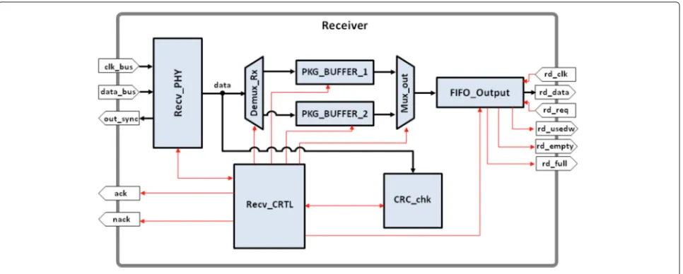
Receiver
The receiver is responsible for capturing the data bus. All signal degradation factors that interfere on the transmis-sion channel, if any, will have their effects reflected in this module’s input signals. Thus, most of the complexity in correcting these effects is located in it.
Fig. 7TRANS_PHYarchitecture. Physical interface of the transmitter
The internal architecture is composed of five modules: the physical layer (RECV_PHY), two FIFOs for receiving
the packages (PKG_BUFFER_1 and PKG_BUFFER_2),
the CRC checker (CRC_CHK), the FIFO output
(FIFO_OUTPUT), and the controller (RECV_CTRL) (Fig. 8).
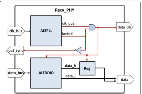
The RECV_PHY module is responsible for receiving the transmitted data and the clock signal from the bus. The entire circuit that implements the DDR standard syn-chronization is also included in this module. A PLL is instantiated internally, and it is responsible for receiving theclock_bussignal and feeding the whole receiver circuit. The PLL used is generated by the MegaWizard tool and is calledALTPLL. This PLL is configured as a synchro-nized source. This means that it guarantees the generated clock to be fully synchronized with the communication bus clock. Figure 9 shows theRECV_PHYarchitecture.
The PLL circuit feeds the receiver through thedata_clk
signal. A locked signal is used to indicate when the PLL reaches synchronism with the input clock. Thus, the
out_syncsignal ensures that transactions can only occur when both the transmitter and receiver are synchronized. In order to minimize the cross-talk effects, this signal was inverted.
The circuit that is responsible for receiving the data packages comprises a demultiplexer (DEMUX_RX), two
FIFOs (PKG_BUFFER_1 and PKG_BUFFER_2), and a
multiplexer (MUX_OUT). Initially, all received data is stored inPKG_BUFFER_1. When the first package is com-plete, its checksum is verified, and if the package is valid, the data may follow to the FIFO output (FIFO_OUTPUT) through MUX_OUT. While this process of transferring
data from the PKG_BUFFER_1 to the FIFO_OUTPUT
occurs,DEMUX_RXswitches and the next captured data begins to be stored in PKG_BUFFER_2. The received package is checked, and if it is valid, the data from this buffer is also transmitted to the same FIFO_OUTPUT
and the DEMUX_RX is switched again. This approach enables one to obtain a higher performance once there is no need to wait for onePKG_FIFO to be transferred to FIFO_OUTPUT to start receiving the next package. FIFOsPKG_BUFFER_1andPKG_BUFFER_2are of 64-bit width and 32-word depth each.
The CRC_CHK module is similar to the CRC_GEN
module in the transmitter. It has the same function and is responsible for calculating the CRC value of the received packages. At the end of each package trans-mission, the checksum value generated byCRC_CHK is compared with the checksum received (generated by the
CRC_GEN). In this structure, if the CRC check fails, the data is discarded before being inserted into FIFO output, and aNACK signal is sent to the transmitter requesting
Fig. 9RECV_PHYarchitecture. Physical interface of the receiver
a retransmission. If the CRC check is positive, the data is routed to FIFO output and an ACK signal is sent to the transmitter requesting the next package.
FIFO output is exactly the same as FIFO input, located in the Transmitter. It works in two different clock domains, and it has configurable depth and width. By default, it has an input data width of 64 bits and an out-put data width of 128 bits with a 256-word depth. The
rd_clksignal corresponds to the clock signal architecture that synchronizes the data readings. Therd_reqsignal is used to read data from FIFO. Therd_usedwsignal indi-cates the data amount inside FIFO to the architecture. The
rd_emptysignal indicates when the FIFO is empty, and the
rd_fullsignal indicates when the FIFO is full.
The RECV_CTRL module generates the control sig-naling to all other modules, thus controlling data pack-age reception, CRC verification, packpack-age transferring from the internal FIFO to the FIFO output, the internal FIFO cleaning in case of error in checksum verification, retransmission request throughNACKsignaling, package reception throughACK signaling, and the demultiplexer (DEMUX_RX) and multiplexer (MUX_OUT) switches.
Dynamic clock phase adjustment
The data captured from the data bus must be done on the most stable moment. This occurs exactly between data transitions. The simplest way to ensure this is by estab-lishing a phase shift in the clock bus to ensure that the clock transition occurs at the desired moment. Figure 10 illustrates that.
A fixed clock phase shift could ensure the timing of the bus clock transition to the data stability time. However, multiplatform FPGAs have particular characteristics -bus width, -bus length, and internal chip features - that generate different timing delays on signal propagation. Thus, it would be virtually impossible to ensure that the data was always captured at the best time. In order to
Fig. 10Data capture in the opposite border. Data capture in the most stable moment
create a flexible communication bus for use in different platforms, a system capable of dynamically configuring and reconfiguring the clock phase when necessary was developed. The configuration is made through the PLL interface that receives the bus clock. Thus, the communi-cation bus proposed in this work is able to self-adapt to the target platform without requiring manual configuration.
The process of identifying and dynamically adjusting the clock phase initiates after the PLL lock. After this step, the transmitter signals the receiver that the dynamic adjustment process has started by asserting high level to
of invalid transmissions, the dynamic adjustment of the clock phase runs again.
Results
The communication channel was tested on a GiDEL PROCStarIII platform connected to an Intel Xeon 3 GHz computer with 4 GB of DDR memory through a PCIex8 bus. Different clock rates and package sizes were tested. Each test was performed considering at least 1 h of continuous data transfer between the FPGAs on the platform.
The data to be transferred is generated by an applica-tion at high level and sent to the host platform through the PCIex8 bus. A specific memory controller from GiDEL (GiDEL PROCMultiPort [15]) is used to transfer the data sent from the application to the transmitter. For testing purposes and correct analysis, the data received by the receiver is sent back to the host, and there, it is compared to the previously sent data.
The times presented in the result tables refer only to the effective data transmission time on the bus. The time of sending data to the host platform, the time to transfer data from the DDR2 memory (located on the platform) to the FPGA transmitter, and the time of data transmission from the receiver on the FPGA to the host were not taken into account.
As a basis for testing, the amount of transferred data during 1 h and a package size of 8 words was adopted. With the data amount transferred in this configuration, it was possible to repeat the tests varying the package size and measuring the transfer time.
Tables 1, 2, 3, and 4 show the results obtained for trans-missions at frequencies of 50, 100, 120, and 150 MHz, respectively.
All the tests with the configurations presented in Tables 1, 2, 3, and 4 were successfully performed, and no transmission error was detected. For all results, a higher data rate was observed when the package size is increased from 8 to 16 words, and then from 16 to 32 words. This occurs due to the clock cycles required to generate and check the CRC at the transmitter and receiver. Once the data package becomes smaller, more cycles will be required to generate the CRC check, conse-quently increasing the overall transmission time. Figure 5 shows a transmission flow for a package size equal to 4 words. Note in the diagram that after sending the
Table 1Results at 50 MHz
Package Transfer rate Data amount Transmission
size (Gbps) (Gb) time (s)
8 0.7 316.65 3600
16 1.14 316.65 ∼2200
32 1.68 316.65 ∼1500
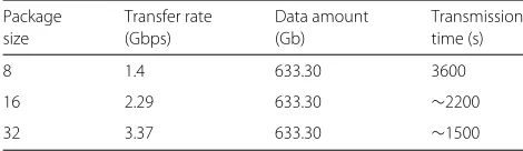
Table 2Results at 100 MHz
Package Transfer rate Data amount Transmission
size (Gbps) (Gb) time (s)
8 1.4 633.30 3600
16 2.29 633.30 ∼2200
32 3.37 633.30 ∼1500
effective data, some data cycles are required to send the CRC.
According to the presented tables, it is possible to see that the data amount transferred increases with the fre-quency. The tests conducted at a frequency of 150 MHz obtained the best transfer rates. For package transmis-sions with a size equal to 8, 16, and 32 words, transmission rates of 1.98, 3.24, and 4.76 Gbps were obtained, respec-tively.
It is important to mention that the same archi-tecture developed and tested in PROCStarIII may have different transmission rates when instantiated on other platforms. Inherent characteristics to the plat-form design can directly influence the communication performance.
Communication error test
In order to test the package retransmission, a module that forces errors in the communication bus was implemented in the architecture. This error generator is positioned at theTRANS_PHY module output and modifies some data bits according to an insertion error rate configured in mil-liseconds. Thus, it is possible to simulate transmission errors and test the operation of the communication bus under these conditions. Such testing ensures the commu-nication bus reliability in an unstable scenario.
In the presented test, one wrong bit was inserted in a period of 4 ms. The transfers were probed at 100 MHz, and the package size was equal to eight words. The amount of transferred data was of 633.30 Gb, the same amount used in the tests at 100 MHz and normal conditions. Table 5 presents the results.
The number of retransmissions performed in this test was of 849,871, indicating that this was the number of packages captured in the receiver that did not match the checksum. Despite the great number of errors, the
Table 3Results at 120 MHz
Package Transfer rate Data amount Transmission
size (Gbps) (Gb) time (s)
8 1.58 715.25 3600
16 2.6 715.25 ∼2200
Table 4Results at 150 MHz
Package Transfer rate Data amount Transmission
size (Gbps) (Gb) time (s)
8 1.98 894.06 3600
16 3.24 894.06 ∼2200
32 4.76 894.06 ∼1500
retransmitted data amount was of just 25.93 Mb, causing no major impacts in relation to the total communication time. The time required for these retransmissions was approximately 144 ms. This time was measured consider-ing the difference between the test with and without error insertion.
After the analysis of these test results, observations showed that the communication was successful despite the errors that had been deliberately inserted in the bus. Therefore, a stable communication between the FPGAs can be obtained under similar conditions.
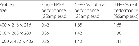
RTM algorithm results
The implemented communication bus was used for pro-cessing the RTM algorithm on the GiDEL PROCStarIII platform. The RTM algorithm is used in the oil and gas industry to generate images of the subsurface helping well exploration identification. This algorithm has high computational cost and therefore needs to be processed on multiple computing units, making it necessary to use four FPGAs of the GiDEL platform in this study case. Tests were performed aiming to validate the communi-cation bus and measure the overhead generated by the communication. As a consequence, the algorithm pre-sented the expected results and the execution time was very close to optimal, which confirms that the commu-nication did not become the bottleneck in the algorithm execution on multiple FPGAs. After that, Table 6 presents these results. The first column lists the size of selected problems, and the following ones are the performance of a single FPGA, optimal performance with four FPGAs, and the actual measured performance, respectively. The performance unit used is of GSamples/s, which corre-sponds to the number of points calculated every second of execution.
Discussion
The presented implementation obtained transfer rates on the order of magnitude of Gbps. At 150 MHz, the com-munication bus achieved transfer rates of up to 4.76 Gbps.
Table 5Error test at 100 MHz clock frequency and 633.3 GB of data transferred
Error insertion Amount of Amount of Retransmission
rate (error/ms) inserted errors retransmitted data (Mb) time (ms)
1/4 849,871 25.93 ∼144
Table 6Results of the RTM algorithm execution on GiDEL platform
Problem Single FPGA 4 FPGAs optimal 4 FPGAs real
size performance performance performance
(GSamples/s) (GSamples/s) (GSamples/s)
400×216×216 0.42 1.68 1.65
300×288×288 0.35 1.42 1.38
1000×432×432 0.35 1.42 1.41
Although the obtained data transfer rates were satisfac-tory, the use of LVDS pins would certainly provide higher data transfer rates. Taking the data presented in [6] as ref-erence, if it was possible to instantiate 32 lanes on the communication bus, each one with rates of 625 Mbps, it would be possible to obtain transfers up to 20 Gbps.
Most modern FPGAs have indicated transceivers for data transfers. Stratix V devices, from Altera, can reach transfer rates up to 28.05 Gbps [16]. However, it is essen-tial that the PCB track routing that will accommodate these devices is done carefully, avoiding communication instabilities.
Conclusions
The use of multi-FPGA platforms enables the applica-tion of performance increase, as multiple reconfigurable devices can be used to perform the same task or work in cooperation. The use of several FPGAs integrated on a single board demands the establishment of a communica-tion channel among such devices.
The presented work describes a bi-directional inter-FPGA communication bus using a DDR interface for data transmission. An architecture was designed as a reconfig-urable platform, requiring only few parameter settings on the transmitter and receiver to port for different configu-rations.
A detection error module was also implemented. It was based on the CRC method and has also a dynamic clock phase shift adjustment in order to ensure a stable communication. The proposed architecture has been tested and validated on the GiDEL PROCStarIII platform.
The proposed communication channel achieved an excellent performance on platforms that do not have advanced features like LVDS interfaces and transceivers. The next step will be to implement it in another plat-form, the GiDEL PROCStarIV. This platform is based on Altera Stratix IV FPGAs and more advanced fea-tures. Thus, the authors expect to achieve higher fre-quencies with the use of the presented communication channel.
Competing interests
Authors’ contributions
All authors have contributed to the different methodological and experimental aspects of the research. All authors read and approved the final manuscript.
Acknowledgements
The authors thank Petrobras for technical support and gratefully acknowledge the continuous support of Gidel, including the availability of prototype boards. The authors also thank FACEPE and CNPq (both Brazilian agencies) for partial financial support.
Author details
1Center for Informatics, Federal University of Pernambuco, Av. Jornalista
Anibal Fernandes, s/n Cidade Universitaria, 50.740-560 Recife, Brazil.2Statistics
and Informatics Department, Federal Rural University of Pernambuco, Rua Dom Manoel de Medeiros, s/n Campus Dois Irmaos, 52.171-900 Recife, Brazil.
Received: 12 March 2014 Accepted: 9 June 2015
References
1. Hammami O, Li X, Larzul L, Burgun L (2009) Automatic design methodologies for MPSOC and prototyping on multi-FPGA platforms. In: SoC Design Conference (ISOCC), International, Busan, Korea. pp 141–146 2. Melnikova O, Hahanova I, Mostovaya K (2009) Using multi-FPGA systems for ASIC prototyping. In: CAD Systems in Microelectronics, 2009. CADSM 10th International Conference - the Experience of Designing and Application of, Lviv-Polyana, Ukraine. pp 237–239
3. Instruments T (2008) LVDS owner’s manual. http://www.ti.com/lit/ml/ snla187/snla187.pdf. Accessed 11 Feb 2014
4. Tiwari A (2012) A low power high speed dual data rate acquisition system using FPGA. In: 2012 International Conference on Communication, Information Computing Technology (ICCICT), Mumbai, India. pp 1–4 5. Huixin Z, Qi H, Suhua L, Haiguang Y (2011) The design for LVDS
high-speed data acquisition and transmission system based on FPGA. In: IEEE 3rd International Conference On Communication Software and Networks (ICCSN), Xi’an, China. pp 383–386
6. Xilinx Inc. http://www.xilinx.com. Accessed 11 Feb 2014 7. Altera Corporation. http://www.altera.com. Accessed 11 Feb 2014 8. Godbole P, Batth A, Ramaswamy N (2010) High speed multi-lane LVDS
inter-FPGA communication link. In: IEEE International Conference OnComputational Intelligence and Computing Research (ICCIC), Coimbatore, India. pp 1–4
9. Inagi M, Takashima Y, Nakamura Y (2009) Globally optimal
time-multiplexing in inter-FPGA connections for accelerating multi-FPGA systems. In: International Conference On Field Programmable Logic and Applications , Prague, Czech Republic, FPL 2009. pp 212–217
10. PARAMNet-3. http://www.cdac.in/html/htdg/products.aspx. Accessed 11 Feb 2014
11. Raptor modules. http://www.ks.cit-ec.uni-bielefeld.de/projects/raptor-family/raptor-modules.html. Accessed 11 Feb 2014
12. GiDEL PROCStarIII. http://www.gidel.com/PROCStarIII.htm. Accessed 11 Feb 2014
13. GiDEL PROCWizard. http://www.gidel.com/procwizard.htm. Accessed 11 Feb 2014
14. Corporation L (2004) DDR interface design implementation. http://www. latticesemi.com/lit/docs/generalinfo/memory_ddr_interface_wp.pdf 15. GiDEL PROCMultiport. http://www.gidel.com/procmultiport.htm.
Accessed 11 Feb 2014
16. Stratix V transceivers. http://www.altera.com/devices/fpga/stratix-fpgas/ stratix-v/transceivers/stxv-transceivers.html. Accessed 11 Feb 2014
Submit your manuscript to a
journal and benefi t from:
7 Convenient online submission
7 Rigorous peer review
7 Immediate publication on acceptance
7 Open access: articles freely available online
7 High visibility within the fi eld
7 Retaining the copyright to your article