www.iosrjen.org
The Role of doping in the window layer on Performance of a InP
Solar Cells USING AMPS-1D
Dennai Benmoussa
1, Hassane Ben Slimane, Hamlaoui Abderrachid
Physics laboratory in semiconductor devices, Department of Physics,University of Bechar, Algeria.
ABSTRACT: - The efficiency of indium phosphide solar cells might be improved by a wide-band-gap window layer. In this work we was simulated using the one dimensional simulation program called analysis of microelectronic and photonic structures (AMPS-1D). In the simulation, hole doping concentration of Ga0.1In0.9P window was varied fro1018 to1020(𝑐𝑚−3). The rest of layer’s doping were kept constant, By varying thickness of window layer the simulated device performance was demonstrate in the form of current-voltage (I-V) characteristics and quantum efficiency (QE).
Keywords: GaInP, AMPS-1D, simulation, conversion, efficiency, quantum efficiency
I. INTRODUCTION
Indium Phosphide has an electronic velocity higher than Silicon but even than GaAs; for this reason it has possible applications in the high frequency range and power electronic devices. It is also characterized by a direct band gap, which encourages its use in optoelectronic devices. It has moreover the highest carriers lifetime among Zinc-blend structures based on III-V [1].
Window layers are quite important in improving the solar cell energy conversion efficiency. They help in effectively reducing the surface recombination at the emitter surface of the solar cell without absorbing the useful light required for the device. Unlike silicon, solar cells based on III-V compound semiconductors and related materials suffer from the lack of native passivating oxides and/or wide choice of suitable large bandgap energy window materials. Various window layer materials have been investigated for III-V compound semiconductor based solar cells [2].
The ternary compound GaxInx-1P is a candidate window layer for InP solar cells, The steep slope of the band gap with change in lattice parameter for Ga0.1In0.9P suggests that a significant increase in window layer transparency could be achieved by only a small eviation of the lattice parameter from the lattice-matched value of 5.86 A.
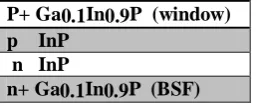
In this present work, a one dimensional simulation program called a analysis of microelectronic and photonic structures (AMPS-1D) [3] is used to simulate the Ga0.1In0.9P window for indium phosphide solar cell structure. Fig. 1 shows the schematic of solar cell design studied in this work. The aim of the simulation of InP solar cell structure was to check the device performance by varying the thickness of the Ga0.1In0.9P window layer. The device performance is mainly based on the material parameters, optical parameters, and electrical parameters of each layers used in the structure. In this simulation the required parameters of Ga0.1In0.9P window having a hole doping concentration1020(𝑐𝑚−3). Twere taken from the elsewhere [4]. For the rest of the
layers the standard parameters were used.
P+ Ga0.1In0.9P (window) p InP
n InP
n+ Ga0.1In0.9P (BSF)
Fig. 1 – InP solar cell structure used for the simulation
II. MODEL DISCRIPTION
function of device length, x. The three main equations are: the Poisson’s equation, continuity equation for free holes, and continuity equation for free electrons. Generally, the Poisson’s equation is [6]:
𝑑
𝑑𝑥 −𝜀 𝑥 𝑑𝜓
𝑑𝑥 = 𝑞 𝑝 𝑥 − 𝑛 𝑥 + 𝑁𝐷
+ 𝑥 − 𝑁
𝐴− 𝑥 + 𝑝𝑡 𝑥 − 𝑛𝑡(𝑥) (1)
Where, ψ is the electrostatic potential, n, p are the concentrations of free electrons and holes, 𝑛𝑡, 𝑝𝑡
are the concentrations of trapped electrons and holes𝑁𝐷+, 𝑁𝐴−are the concentrations of ionized donors and
acceptors, ε is the dielectric permittivity of semiconductor, and q is the electron charge.
The transport characteristics of an electronic device may be derived by the continuity equation for the holes and electrons. The continuity equations in steady state conditions are:
1 𝑞
𝑑𝑗𝑛
𝑑𝑥 = 𝑅𝑛 𝑥 − 𝐺 𝑥 , (2) 1
𝑞 𝑑𝑗𝑝
𝑑𝑥 = 𝐺 𝑥 − 𝑅𝑛𝑝 𝑥 3
Where, 𝐽𝑛, 𝐽𝑝 are electron and hole current density, 𝑅𝑛, 𝑅𝑝 are electrons and holes recombination
velocities for direct band-to-band and indirect transitions, and G is the optical generation rate which is expressed as a function of 𝑥 is,
𝐺 𝑥 = − 𝑑 𝑑𝑥 𝜙𝑖
𝐹𝑂𝑅 𝜆 𝑖 +
𝑑 𝑑𝑥 𝜙𝑖
𝑅𝐸𝑉 𝜆 𝑖 𝑖
𝑖
(4)
where, 𝜙𝑖𝐹𝑂𝑅and 𝜙𝑖𝑅𝐸𝑉 are, respectively, the photon flux of the incident light and the light reflected
from the back surface at a wavelength, λ of 𝑖 at some point 𝑥, depending on the light absorption coefficient, and the light reflectance in the forward and reverse direction. In our simulation, the reflection indices for the forward and reverse directions are 0 and 0.6, respectively. The governing equations (1), (2), and (3) must hold at every position in a device, and the solution to these equations involves determining the state variables 𝜓(𝑥), the 𝑛 -type quasi-Fermi level 𝐸𝑓𝑛, and the 𝑝 -type quasi-Fermi level 𝐸𝑓𝑝 or, equivalently, 𝜓(𝑥), 𝑛(𝑥),and 𝑝(𝑥),, which
completely defines the system at every point 𝑥. Because the governing equations for 𝜓(𝑥), 𝐸𝑓𝑛, and 𝐸𝑓𝑝 are
non-linear and coupled, they cannot be solved analytically. There must be boundary conditions imposed on the set of equations.
The Newton-Raphson technique is used in AMPS-1D. To be specific, the solutions to equations (1), (2), and (3) must satisfy the following boundary conditions:
𝜓 0 = 𝜓0− 𝑉;
𝜓 𝐿 = 0;
𝑗𝑝 0 = −𝑞𝑆𝑃0 𝑝0 0 − 𝑝 0 ; (5)
𝑗𝑝 𝐿 = −𝑞𝑆𝑃𝐿 𝑝 𝐿 − 𝑝0 𝐿 ;
𝑗𝑛 0 = −𝑞𝑆𝑛0 𝑛 0 − 𝑛0 0 ;
𝑗𝑛 𝐿 = −𝑞𝑆𝑛𝐿 𝑛0 𝐿 − 𝑛 𝐿
𝑆𝑃0, 𝑆𝑝𝐿, 𝑆𝑛0 𝑎𝑛𝑑 𝑆𝑛𝐿 appearing in those conditions are effective interface recombination speeds for holes and
electrons at 𝑥 = 0, and 𝑥 = L.
AMPS-1D solves three coupled differential equations each subject to boundary conditions (equation. 5) and then calculates the electrostatic potential and the quasi-Fermi level for holes and electrons at all point in the solar cell. Once these values are known as a function of depth, it is straightforward to calculate the carrier concentrations, electric fields and currents, and device parameters like the open-circuit voltage(𝑉𝑜𝑐), short-circuit current density (𝐽𝑠𝑐), fill-factor (𝐹𝐹), and the efficiency (𝜂). These parameters define the performance of a solar cell.
Front Contact Windows
Back Contact BSF
PHIBO SNO
1.36 1.00E+07
PHIBL SNL
0.035 1.00E+03 SPO
RF
1.00E+07 0
SPL RB
1.00E+03 1
III. EXPERIMRNTAL
In this study, a one-dimensional numerical analysis tool, AMPS-1D, is used to create various solar cell models and obtain its results. In AMPS-1D, four different layers are required for the modeling. More layers can be added as long as the grid points do not exceed the limitation, viz. 200-grid points. The four layers that are used in this modeling is the P+ Ga0.1In0.9P (window), p - InP, n-InP and n+ Ga0.1In0.9P (BSF). Table 1 and table 2 show the description for the parameters used in the simulation and the base parameter that are used throughout the study [10].
Layers Parameters
P+ Ga0.1In0.9P p - InP n-InP n+ Ga0.1In0.9P
Thickness(nm) 100 200 500 100
Dielectricconstant,ε 12.36 12.50 12.50 12.36
Electron mobility 𝜇𝑛
(cm²/Vs)
1100 4000 4000 1100
Hole mobility 𝜇𝑝
(cm²/Vs)
35 150 150 35
Carrier density, 𝑛 𝑜𝑟 𝑝 (𝑐𝑚−3)
P:1E18-1E20 P:5E16 n:5E16 n:1E19
Optical band gap,𝐸𝑔
(eV)
1.39 1.35 1.39
Effective density,𝑁𝑐
(𝑐𝑚−3)
3.89E+19 5.7E17 5.7E17 3.89E+19
Effective density,𝑁𝑣
(𝑐𝑚−3)
2.93E+19 1.1E19 1.1E19 2.93E+19
Electron affinity ,χ(eV) 4.33 4.38 4.38 4.33
Table 1:AMPS-1D parameters InP solar cell
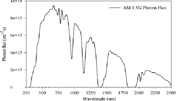
The AM 1.5 G photon flux was used for the illumination (Fig. 2). The number of incident photons / (cm²/s) was entered for wavelengths between 0.320 (µm) to 940 (µm), with a step size of 2 nm. The front panel of AMPS-1D simulation for InP solar cell structure is shown in Fig. 3.
Fig. 3 – AMPS simulation front panel contains the device and layer grid parameters, and general layer parameters
IV. RESULTS AND DISCUSSIONS
For that presented simulation, we have chosen a range of hole doping concentration between 1018
to1020(cm−3) for window layer. The figure 4 schematizes the illuminated characteristics J-V of InP solar cell.
According to these results, we notice a maximal density of current (30.303mA/cm2) for a value of the doping of the window layer Na = 1018 (cm−3) but for a maximal voltage (1.104V) for a value of the doping of the
Window layer1020(cm−3).
Fig. 4: The effect of doping of the window on the characteristics J-V
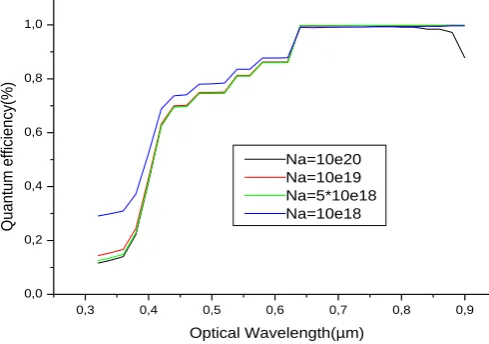
The spectral response (QE) for different thicknesses window from AMPS-1D simulation is shown in fig. 4; the cell with window layers of the doping 1020(cm−3).maintains almost above 99% of QE for the whole
visible range of spectra where it is confirmed better energy conversion performance of the cell.
0,3 0,4 0,5 0,6 0,7 0,8 0,9
0,0 0,2 0,4 0,6 0,8 1,0
Q
uant
um
ef
ficienc
y(%)
Optical Wavelength(µm) Na=10e20 Na=10e19 Na=5*10e18 Na=10e18
0,0 0,2 0,4 0,6 0,8 1,0 1,2
0 5 10 15 20 25 30
Cu
rre
nt De
nsity
(mA/
cm²)
voltage(V) Na=10e+20
The effect of the doping window layer on cell performance such as effect on general performance parameters, quantum efficiency (QE), shunt and series resistance, light and dark I-V characteristics. Characteristics of each cell with window a thickness are shown in the Table
Thickness of window 𝐽𝑠𝑐(𝑚𝐴 𝑐𝑚²) 𝑉𝑜𝑐(𝑉) 𝐹𝐹% 𝐸𝑓𝑓%
Na=10e+18 30.303 0.850 85.8 22.114
Na=5*10e+18 29.795 0.897 87.0 23.257
Na=10e+19 29.744 0.928 87.5 24.156
Na=10e+20 29.489 1.104 89.0 28.986
V. CONCLUSIONS
We used AMPS-1D to investigate the dependence of the thickness window layer(Ga0.1In0.9P ) for InP solar cells. We demonstrated the effect of doping in window layer on the parameters of solar cells as open-circuit voltage (Voc), the short-open-circuit current density (𝐽𝑠𝑐), the conversion efficiency 𝐸𝑓𝑓 the quantum
efficiency (QE). The conversion efficiency increased until hole doping concentration of Ga0.1In0.9P reaches around 1020(𝑐𝑚−3). Further increase of doping shows no improvement in efficiency. Similarly QE response is
almost overlapping after the 1020(𝑐𝑚−3)toping layer window. These observations led to the conclusion that for
the optimal performance of the solar cell device the hole doping concentration of layer plays a role.
Acknowledgements
We would like to acknowledge the use of AMPS-1D program that was developed by Dr. Finish’s group at Pennsylvania State University (PSU).
REFERENCES
[1] M. Yamaguchi, C. Uemura and A. Yamamoto, J.Appl. Phys., 55, pp. 1429, 1984.
[2] J. Lammasniemi, R. K. Jain, M. Pessa, “Status of Window Layers for III-V Semiconductor Cells”,Proceedings 14th European Photovoltaic Solar Energy Conference (1997) p. 1767.
[3] S.J. Fonash, A manual for One-Dimensional Device Simulation Program for the Analysis of Microelectronic and Photonic Structures (AMPS-1D), (The Center for Nanotechnology Education and Utilization, The Pennsylvania State University, University Park, PA 16802).
[4] M. J. Ludowise, W. T. Dietze, R. Boettcher and N. Kaminar, “High-Efficiency (21.4%) Ga0.75In0.26As/GaAs (Eg=1.15 eV) Concentrator Solar Cells and the Influence of Lattice Mismatched on Performance”, Appl. Phys. Lett., Vol. 43, p. 468 (1983). [5]. S.M. Sze Physics of semiconductor devices (New York: John Wiley & Sons Press: (1981).