Generation and performance of localised surface plasmons utilising
nano-scale structured multi-layered thin films deposited upon
D-shaped optical fiber
T. Allsop
*a, R. Neal
b, C. Mou
a, M. Dvorak
c,
A. Rozhin
aK. Kalli
d, D.J. Webb
a aAston Institute of Photonic Technologies, Aston University, Aston Triangle, Birmingham, B47ET,
UK;
b
Dept of Maths and Computing, and the Faculty of Science and Technology, University of
Plymouth, Plymouth, PL4 8AA, U.K;
c
Institute of Physical Engineering/CEITEC, Brno University of Technology, Technická 2/10, Brno
616 69, Czech Republic;
d
Cyprus University of Technology, 31 Archbishop Kyprianos, Lemessos 3036, Cyprus
ABSTRACT
A new generation of surface plasmonic optical fibre sensors is fabricated using multiple coatings deposited on a lapped section of a single mode fibre. Post-deposition UV laser irradiation using a phase mask produces a nano-scaled surface relief grating structure, resembling nano-wires. The overall length of the individual corrugations is approximately 14 m with an average full width half maximum of 100 nm. Evidence is presented to show that these surface structures result from material compaction created by the silicon dioxide and germanium layers in the multi-layered coating and the surface topology is capable of supporting localised surface plasmons. The coating compaction induces a strain gradient into the D-shaped optical fibre that generates an asymmetric periodic refractive index profile which enhances the coupling of the light from the core of the fibre to plasmons on the surface of the coating. Experimental data are presented that show changes in spectral characteristics after UV processing and that the performance of the sensors increases from that of their pre-UV irradiation state. The enhanced performance is illustrated with regards to change in external refractive index and demonstrates high spectral sensitivities in gaseous and aqueous index regimes ranging up to 4000 nm/RIU for wavelength and 800 dB/RIU for intensity. The devices generate surface plasmons over a very large wavelength range, (visible to 2 μm) depending on the polarization state of the illuminating light.
Keywords: Keywords: Structured thin films, Nano-scale, Localised surface plasmons, Optical fibre,
Optical fibre sensing
*[email protected]; phone 44 (0) 0121 204 3484
1.
INTRODUCTION
Optical fibre has become one of the preferred optical platforms to conduct research into optical sensing [1] due to ease of interrogation along with integration with other optical components, which has been driven by the telecoms industry. Various kinds of optical mechanisms have been investigated with one of the motivations being to produce environmental sensing capabilities [2], including potential applications in chemistry, biochemistry and biology [3-5]. One of these
physical phenomena that is being used commercially and continues to be a topic for research is surface plasmons and
their spectral resonances [6-9], which have been found to be very sensitivity to localized environmental changes (change
in refractive index of the surrounding material). The surface plasmon resonance is an important optical phenomenon that
surface Plasmon (LSP) [11]. More recently there has been a focus on localized surface plasmons being generated by various surface topologies and materials (structured thin films) which in turn govern the optical and physical characteristics of the plasmons being generated. The complex spectral behaviour of these LSPs is determined by many physical dependencies, for example on the size, topology and geometries of the plasmon-supporting nanostructures. Examples of the effects of surface topology on the spectral behaviour of plasmons can easily be found in the literature [11]. The optical properties and characteristics of structured thin film can be comprehensively tuned by nano-engineering the structure parameters, such as using periodically arranged nanopores or microporous and nanoporous metal structures [11, 12, 13, 14].
We report on the fabrication and characterisation of SPR fibre devices that use a lapped, D-shaped single-mode optical fibre on which is deposited multiple thin film layers of materials consisting of metals, semiconductors and oxides. Using UV laser irradiation along with a phase mask produces a nano-scaled surface relief grating structure, which resembles an array of nano-wires on the flat of the D-shape fibre. This nano-scaled surface relief grating corrugation is the result of structure compaction of the multi-layered coating. Evidence will be presented to support the suggestion that this structural compaction induces a periodic strain gradient into the D-shaped optical fibre that generates an asymmetric refractive index profile which enhances the coupling of the light from the core of the fibre to plasmons on the surface of the coating. Furthermore, experimental data are presented that show changes in spectral characteristics after and during UV processing and that there is an resultant enhancement in their spectral sensitivity. The enhanced performance is illustrated with regards to change in external refractive index and demonstrates high spectral sensitivities in gaseous and aqueous index regimes ranging up to 4000 nm/RIU for wavelength and 800 dB/RIU for intensity. The devices generate surface plasmons over a very large wavelength range (visible to 2 μm), depending on the polarization state of the illuminating light.
2.
FABRICATION OF THE ST
5
UCTURED THIN FILM COATING
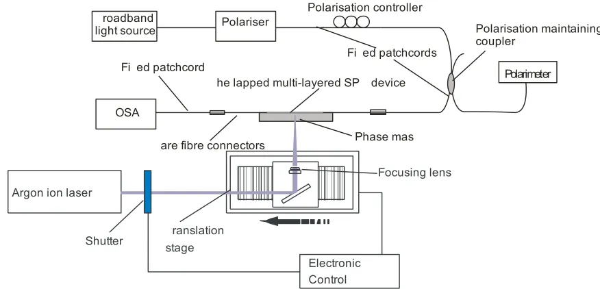
The device is constructed in three stages [15]. Firstly, a standard single mode optical fibre (SMF-28) is mechanically lapped down to within 5m ±0.5m from the core-cladding interface. This distance is large enough to minimise the evanescent field strength at the flat of the lapped fibre surface and to stop the coated flat of the D-shaped acting as a “mode sink” which would affect the overall dynamic range (optical power) of the sensor, see figure 1.Secondly, vacuum RF plasma sputtering is used to deposit a series of thin film coatings onto the flat region of the lapped fibre. The materials used for these coatings were germanium (48nm), silicon dioxide (48nm) and either gold, silver or platinum (32nm for platinum, 36nm for silver, 34m for gold), seefigure 2. The various thicknesses were estimated by means of a witness plate. The third stage is to expose the D-shaped fibre to a UV light interference pattern generated from a commercial uniform phase mask with a period of 1.018m along the length (typical 2.2cm) of the fibre with the coating with the flat of the D-shape fibre facing the phase mask, see figure 2. The UV irradiance is produced by an argon ion laser (Innova® Sabre® FRED) operating at 244nm. Typical fabrication parameters used are a scanning velocity of 0.05mms-1 and a UV optical power on the fibre itself of approximately 84mW. The surface plasmon resonances were monitored during the fabrication of the structured thin film on the fibre; a schematic of the apparatus is shown in figure 1. A polariser and polarisation controller are used to maximise coupling to the surface plasmon.Light from a broadband light source was passed through the polariser and a polarisation controller before illuminating the sample, with the transmission spectrum being monitored using an optical spectrum analyser. The change in polarisation of the illuminating light was monitored with a polarimeter (Tektronix, PAT 9000B) through a polarisation maintaining coupler, see figure 1.
that of nano-wires are surrounded by dielectric materials; the supporting SiO2 layer beneath the metal layer and the surrounding environment elsewhere..
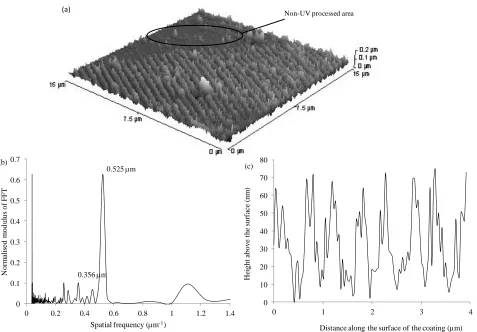
The dimensions of the structures vary with UV dosage, exposure and materials used in the construction of the coating; figure 4 shows results obtained with a platinum metal overlay. The overall length of the individual corrugations with this sample is approximately 14 m with an average FWHM of 100 ± 20 nm, thus the length of the uniform perturbation is again approximately 2 orders of magnitude greater in size than the width and there appears to be a more uniform structure. The dimensions of these Pt nano-wires are determined from the AFM data and have an approximate base length of 73nm ± 14 nm and a height of the 32nm± 2 nm.
Polarisation controller Broadband
light source Polariser
OSA
Fixed patchcord
Fixed patchcords
Bare fibre connectors
The lapped multi-layered SPR device Polarimeter
Phase mask
Argon ion laser
Electronic Control Shutter Translation
stage
Focusing lens
Polarisation maintaining coupler
Figure 1. Schematic of the apparatus used to fabricate the structured thin film coating
7
3
.1
3
m
Gold
Germanium Silica
Combinations of multi-layers used
(C)
(B)
(A)
Lapped cladding region of fibre Multi coatings
Phase mask UV (244nm) light
(a)
(c)
(b)
Core location
Image of a lapped
SMF fibre
0.525 m
0.356 m
0 0.1 0.2 0.3 0.4 0.5 0.6 0.7
0 0.2 0.4 0.6 0.8 1 1.2 1.4
N
or
m
al
is
ed
m
od
ul
us
of
F
F
T
Spatial frequency (m-1)
0 10 20 30 40 50 60 70 80
0 1 2 3 4
H
ei
ght
a
bov
e t
he
s
ur
fa
ce
(
nm
)
Distance along the surface of the coating (m)
(b) (c)
Non-UV processed area
(a)
Figure 3 (a) Three dimensional view of the AFM data showing the surface topology of the flat of the D-shaped fibre with a gold metal overlay coating, showing a section of UV processed and non-processed coating .. (b) A line profile across the surface of the device that has been UV processed. (c) A fast Fourier transform (FFT) of the typical AFM line profile of the post-UV processed coating.
0 5 10 15 20 25 30 35
0 1 2 3 4 5 6
H
ei
ght
a
bove
t
he
s
ur
fa
ce
(
nm
)
Distance along the surface of the coating (m)
Figure 4. Typical line profile across the surface of the device with a platinum metal overlay that has been UV processed. Data obtained from AFM analysis.
illumination of the Ge and SiO2 layers in our device produces a surface corrugation due to this compaction. X-ray
photoelectron spectroscopy (XPS) is a quantitative spectroscopic technique that analyses the surface of a material,
measuring the elemental composition and chemical state of the elements that exist in the surface region by determining the binding energies of their electrons. This technique was used to investigate the coating material and detected the presence of germanium oxides which are known to produce the structural change in the material [15, 17]. Therefore the generation of the observed surface topology suggests that the compaction creates a quasi-periodic strain field in the coating and the fibre substrate that extends into the core, which then acts to couple light from the core into the surface
plasmon mode. This can be understood as an asymmetric radial refractive index profile and can be visualised as the
equivalent of a fibre subjected to bending.
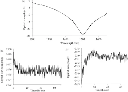
To look for evidence that a quasi-periodic strain field is generated by these coatings, the gold metal overlay
device was annealed at 80oC. The response of the device in transmission is shown in figure 5 for a constant temperature
of 80oC (for a polarisation tuneable resonance at 1500nm, shown in figure 5(a)). Initially the spectral feature red shifted
by 19.5±0.5nm, as the temperature increased. This spectral behaviour was followed by a slower annealing process with a blue wavelength shift of approximately 3.7nm and a reduction in the optical strength of 3dB. It is known that the strength
of the grating is given by 1-tanh2(n/B), where represents the fraction of fibre mode power contained by the fibre’s
core and can be estimated using the normalised V parameter andB= 2neffwhere neff is mainly caused by composition of the fibre core along with a small but significant change in refractive index generated from the residual stress after inscription. This low temperature annealing is characteristic of the behaviour of a standard type I UV inscribed grating and provides evidence of a grating structure in the core [17].
-25 -20 -15 -10 -5 0
1200 1300 1400 1500 1600
O
pt
ic
al
s
tr
eng
th (
d
B
)
Wavelength (nm)
(a)
1493 1494 1495 1496 1497 1498 1499 1500
0 20 40 60
Ce
n
tra
l
w
a
v
el
e
n
g
th
(n
m
)
Time (Hours) (b)
-24.5 -24.3 -24.1 -23.9 -23.7 -23.5 -23.3 -23.1 -22.9 -22.7 -22.5
0 20 40 60
O
p
ti
c
a
l
st
re
n
g
th
(d
B)
Time (hours) (c)
3.
SENSING SPECTRAL CHARACTERISICS
The spectral sensitivity to refractive index and polarisation of the transmission spectral features of the fibre devices were investigated before, during and after formation of this structure. Figure 1 shows the experimental set-up used for polarisation characterisation both during fabrication and when the fibre devices were submerged into various liquids with different refractive indices. Light from a broadband light source was passed through a polariser and a polarisation controller before illuminating the sample, with the transmission spectrum being monitored using an optical spectrum analyser. The change in polarisation of the illuminating light was monitored with a polarimeter (Tektronix, PAT 9000B) through a polarisation maintaining coupler, see Figure 1.The noise and spectral artifacts exhibited in the transmission spectra in Figure 6 are due to the detection limits of the optical spectrum analyser and the spectral profile of the associated broadband light source.
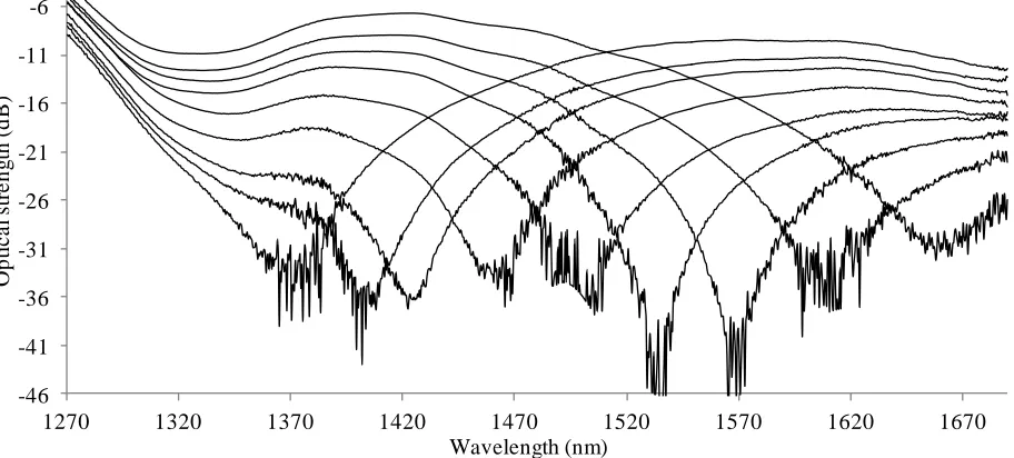
After UV processing, the first observation is that many more LSP resonances can exist, and by varying the polarization state of the illuminating light they can be tuned over an extremely broad wavelength range from 1000nm to 2000nm, depending upon the metal overlay used. This spectral tuning ability is shown in figure 6 for platinum each transmission spectra observed is a given polarisation state..
-46 -41 -36 -31 -26 -21 -16 -11 -6
1270 1320 1370 1420 1470 1520 1570 1620 1670
O
p
ti
c
a
l
st
re
n
g
th
(d
B)
Wavelength (nm)
Figure 6. The observed surface plasmon resonances obtained at different wavelengths by varying the polarization state of the illuminating light for the device consisting of Pt-SiO2-Ge.
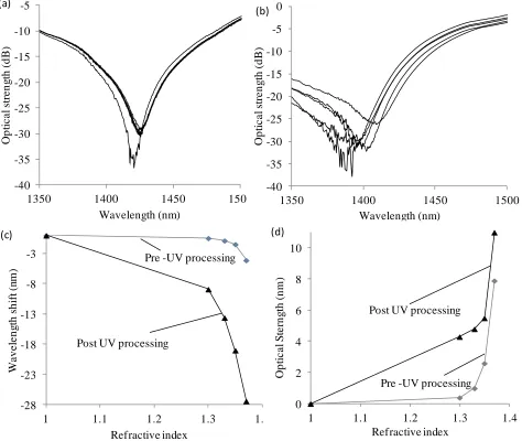
aqueous index regime are achievable. Secondly, the main spectral feature occurs at a different wavelength after UV processing; this suggests from the theory of SPR [10] that the coating topology has changed and/or the overall thickness has changed. Effectively the UV process transforms the initially planar surface supporting conventional surface plasmons into effectively an array of metallic nano-rods lying along the tops of the surface grooves. Such a structure supports localised surface plasmons that have different dispersive properties and hence different resonance conditions, which accounts for the increased sensitivity and its different sign for wavelength shift.
-40 -35 -30 -25 -20 -15 -10 -5
1350 1400 1450 1500
O p ti c a l st re n g th (d B) Wavelength (nm) (a) -40 -35 -30 -25 -20 -15 -10 -5 0
1350 1400 1450 1500
O p ti c a l st re n g th (d B) Wavelength (nm) (b) -28 -23 -18 -13 -8 -3
1 1.1 1.2 1.3 1.4
W a v e le n g th s h ift (n m ) Refractive index (c)
Post UV processing
Pre -UV processing
0 2 4 6 8 10
1 1.1 1.2 1.3 1.4
O p ti c a l S te rn g th (n m ) Refractive index Pre -UV processing Post UV processing (d)
Figure 7. The spectral transmission profiles for increasing index of the surrounding medium (a) Au-SiO2-Ge SPR fibre device as a function of index prior to UV processing and (b) post-UV processing. (c) Shift in central wavelength and (d) optical strength as a function of refractive index of the spectral feature before and after UV processing
4.
CONCLUSION
the platinum and 180nm for the gold overlay metallic layer withheights of 32nm and 70nm respectively. We have presented annealing data that gives evidence that these surface structures result from material compaction created by the silicon dioxide and germanium layers in the multi-layered coating and the surface topology is capable of supporting localised surface plasmons. Therefore this change in surface topology fundamentally changes the spectral characteristics of the surface plasmons being generated. This fact is supported by experimental data presented that shows the increase in spectral sensitivity to environmental parameters following UV exposure.
5.
ACKNOWLEDGMENT
This work is funded by EPSRC Joint Research Grant: EP/J010413/1 Title: Grating and waveguide plasmonic sensors. Also we would like acknowledge that some funding came from European Regional Development Fund (CEITEC-CZ.1.05/1.1.00/02.0068) and the EU 7th Framework Programme (SYLICA and 280566 - UnivSEM).
REFERENCES
[1] Lee, B., "Review of the present status of optical fiber sensors." Optical Fiber Technology 9(2), 57-79 (2003). [2] Bhamber, R. Allsop, T. Lloyd, G. Webb, D. J. Ania-Castanon, J. D., “Arbitrary real-time three dimensional
corporal object sensing and reconstruction” Optics Letts. 37(17), 3549-3551 (2012).
[3] Wolfbeis, O. S., “Fibre-optic sensors in biomedical sciences” Pure and Applied Chemistry 59(5), 663-672 (1987).
[4] Allsop, T. Zhang, L. Bennion, I. "Detection of organic aromatic compounds in paraffin by a long period fiber grating optical sensor with optimised sensitivity" Opt. Comm. 191(3), 181-190 (2001).
[5] Vasilev, S. Medvedkov, O. I., “Long-period refractive index fibre gratings: properties, applications and fabrication techniques” Proc. SPIE 4083, 212-223 (2000).
[6] Slavík, H.Homola, J., “Ultrahigh resolution long range surface plasmon-based sensor” Sensors and Actuators B 123(1), 10-12 ( 2007).
[7] Allsop, T. Neal, R. Mou, C. Saied, S. Rehman, S. Kalli, K. Webb, D. J. Sullivan, J. Mapps, D. Bennion, I., “The exploitation of multilayer coatings for infra-red surface plasmon resonance fibre sensors” Appl. Optics 48(1), 276–286 (2009).
[8] Brolo, A. R. Gordon, R. Leathem, B. Kavanagh, K. L., “Surface plasmon sensor based on the enhanced light transmission through arrays of nanoholes in gold films,” Langmuir 20, 4813 (2004).
[9] Dhoa, X. Kirk, A. G. Tabrizian, M., "Towards integrated and sensitive surface plasmon resonance biosensors: a review of recent progress," Biosensors and Bioelectronics 23(2), 151-160 (2007).
[10] H. Raether, [Surface Plasmons on smooth and Rough Surfaces and on Gratings], Academic, New York, (1997).
[11] E. Hutter, H. Eliza, J. Fendler, H. J.,. "Exploitation of localized surface plasmon resonance," Advanced Materials 16(19), 1685-1706 (2004).
[12] Haes, A. J. Van Duyne, A. R., “Unified view of propagating and localized surface plasmon resonance biosensors,” Anal. Bioanal. Chem. 379, 920-925 (2004).
[13] Skigin D. C., M. Lester, M, “Study of resonant modes of a periodic metallic array near a dielectric interface: evanescent-to-propagating coupling via surface plasmon excitation,” J. Opt. A: Pure Appl. Opt. 8, 259–267 (2006).
[14] Kucheyev, S. O. Hayes, J. R. Biener, J. Huser, T. Talley, C. E. Hamza. A. V., "Surface-enhanced Raman scattering on nanoporous Au," Applied physics letters 89(5), 053102-053102 (2006).
[15] Allsop, T. Neal, R. Mou, C. Saied, S. Rehman, S. Kalli, K. Webb, D. J. Culverhouse, P. F. Sullivan, J. Mapps, D. Bennion, I., “Formation and characterisation of ultra-sensitive surface plasmon resonance sensor based upon a nano-scale corrugated multi-layered coated D-shaped optical fibre,” Jn. Quantum Electron. 48(3), 394 – 405 (2012).
[16] Williams, D. J. Davey, S.T. Kashyap, R. Armitageand, J.R. Ainslie, B.J., “ UV spectroscopy of optical fibres and performs,” Proc. Soc. Photo. Opt. Instrum. Eng. 1516, 29 (1991).