IJIRT 100044
INTERNATONAL JOURNAL OF INNOVATIVE RESEARCH IN TECHNOLOGY11
Comparative Analysis of Vedic Multiplier by Using
Different Adder Logic Style at Deep Submicron
Technology
Er. Mandeep Singh, Er. Candy Goyal
Deptt. Electronics & Communication Eng.
Yadwindra College of Engg. Talwandi Sabo Bathinda
Abstract- In the recent years growth of the portable electronic is forcing the designers to optimize the existing design for better performance. Multiplication is the most commonly used arithmetic operation in various applications like DSP processor, math processor and in various scientific arithmetic circuits. Overall performance of the VLSI system is strongly depends on the performance of arithmetic circuits like multiplier. Different types of multiplier are available in the literature depending on the requirement. Designer used different type of multiplier. Power consumption in a multiplier is more prominent design factor in addition with the performance, because portable equipment needs larger battery backup which is only possible through low power design. This work focuses on the reduction of the power dissipations which is showing an ever-increasing growth with the scaling down of the technologies. The power consumption is an important issue that has lead to multiplier designer to adopt different technique to reduce power dissipations. In this thesis work, a Vedic algorithm is used to reduce the power consumption in multiplier used. This work focus on the analysis of power dissipation, delay, area of Vedic Multiplier using different adder logic style at 180nm technology by using tanner EDA tool.
I.
INTRODUCTIONDigital multiplication is one of the most basic functions in arithmetic circuits. The ubiquity of this operation in computing has given rise to a large number of multiplier implementations, each with different specifications and goals. Some applications require wide dynamic range, others need high precision, while in some cases, neither of these characteristic is very tightly specified. Digital multiplication is used as
Opposed to analog when high precision is an issue; it is fairly straightforward to make digital
Multipliers are accurate as the application requires. Precision required for multiplication
Varies by function. The basic operation in these designs is integer multiplication. In floating
Point multipliers, integer multiplication units are sub-blocks of the greater floating point unit. Signed versus unsigned techniques have an impact on the design, and some other techniques have been suggested for manipulating the bit representation of
numbers to generate power savings. However, the primary consideration in multipliers has been and continues to be delay. The demand for high speed processing has been increasing as a result of expanding computer and signal processing applications. Higher throughput arithmetic operations are important to achieve the desired performance in many real-time signal and image processing applications [1]. One of the key arithmetic operations in such applications is multiplication and the development of fast multiplier circuit has been a subject of interest over decades. Reducing the time delay and power consumption are very essential requirements for many applications. This work presents Vedic multiplier with different circuit style of adder. Multiplier based on Vedic Mathematics is one of the fast and low power multiplier.
Need for Vedic Mathematics:-
It consumes the less time.
It reduces the scratch from finger.
It is magical tool for the calculations.
It provides the one line answer.
It gives the more concentrations to works.
II. PRESENT WORK
Vedic Mathematics: - The proposedVedic multiplier
is based on the Vedic multiplications formulae (Sutras). This Sutra has been traditionally used for the multiplications of two numbers in the decimal number system. In this work we apply the same ideas to the binary number system to make the proposed algorithm compatible with the digital hardware. Vedic multiplications based on some algorithm, one of them is discussed below:
IJIRT 100044
INTERNATONAL JOURNAL OF INNOVATIVE RESEARCH IN TECHNOLOGY12
done with the concurrent additions of these partialproducts. The parallelism in generations of partial products and their summations is obtained using Urdhava Triyakbhyam in fig 1. Since the partial products and their sum are calculated in parallel, the multiplier is independent of the clock frequency of the processor. The net advantage is that it reduces the need of microprocessor to operate at increasingly high clock frequency. While a higher clock frequency generally results in increased processing power, its disadvantage is that it also increases power dissipations which results in higher device operating temperature. By adopting the Vedic multiplier, microprocessors designer can easily circumvent these problem to avoid catastrophic device failures.
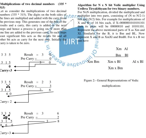
Multiplications of two decimal numbers (335 * 315)
Let us consider the multiplications of two decimal numbers (335 * 315). The digits on the both sides of the lines are multiplied and added with the carry from the previous step. This generates one of the bits of the results and a carry, this carry is added in the next steps and hence a process is going on. If more than one line are added to the previous carry. In each steps least significant bits acts as the results bit and all other bit acts as carry for the next step. Initially the carry is taken to be zero.
3 3 5 Result = 3 0
Pre Carry = 0
3 1 5 3 0
0
Carry=3
3 3 5 Result = 2 3
Pre Carry = 3
3 1 5 2 6
6 0
Carry= 2
3 3 5 Result = 3 6
Pre Carry = 2
3 1 5 3 8
8 6 6
Carry=3
3 3 5 Result = 1 2
Pre Carry = 3
3 1 5 1 5
5 8 6 0
Carry=1
3 3 5 Result = 0 9
Pre Carry = 1
3 1 5 10
10 58 60
Fig.1:- Multiplications of two decimal numbers by Urdhva Tiryakbhyam
Algorithm for N x N bit Vedic multiplier Using Urdhva Tiryakbhyam for two binary numbers. For NxN multiplication, divided the multiplicand and multiplier into two parts, consisting of (N to N/2-1) bits and (N/2) bits. For example for multiplications of X and B, of 16 bits each, if X=0000001010101101 then its parts will be 00000010 and 10101101. Represent the above mentioned parts of X as Xm and Xl. Similarly for the B, it is Bm and BL. Now represent X and B as XmXl and BmBl. For A x B we can have
Xm Al
Bm Bl
Xm Bm Xm x Bl Al x Bl
Xm x Bm
Figure 2:- General Representations of Vedic
IJIRT 100044
INTERNATONAL JOURNAL OF INNOVATIVE RESEARCH IN TECHNOLOGY13
Fig 3:- Complete block diagram for n x n bit Vedicmultiplier
III. MULTIPLIER DESIGN
Schematics of different blocks of multiplier design: - The schematics of different blocks of multiplier design are designed on the TANNER tool by using 180um technology.
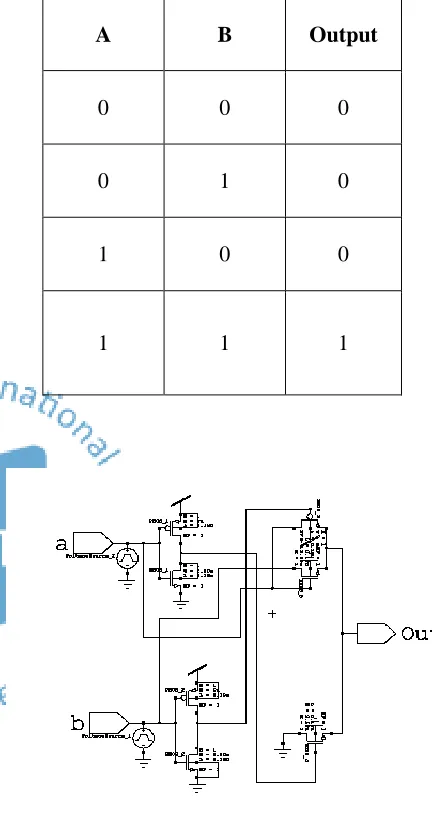
Schematic of AND Gate:- In multiplier design, first
of all product terms will be generated using AND gates and then these product terms will be added using adders to get the result as explained in earlier chapters. Product term is an AND operation between A bit of one number and the B bit of a second number. If both the inputs to the AND gate are HIGH (1), then a HIGH output (1) results. A LOW output results, if neither or only one input to the AND gate is HIGH. In another sense, the function of AND effectively finds the minimum between two binary digits, just as the OR function finds the maximum. Thus, the output is always 0 except when all the inputs are 1s. The operational truth table of an AND gate is shown in table 4.1 where A, B are the inputs of AND gate and while its schematic is shown in figure 4.3.
Table 1: Truth Table of AND Gate
A
B
Output
0
0
0
0
1
0
1
0
0
1
1
1
Figure 4:- Schematic of AND Gate
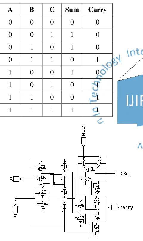
Schematic of Full adder
Basically the Full Adder is type of combinational circuit. The Full Adder are used to overcome the disadvantage of half adder. It will perform the full additions of numbers. The addition of the partial product terms is done with full adder which are generated by AND Gate. The full adder adds binary numbers. A one-bit full adder adds three one-bit numbers, often written as A, B, and Cin; A and B are
the operands, and Cin is a bit carried in from the next
IJIRT 100044
INTERNATONAL JOURNAL OF INNOVATIVE RESEARCH IN TECHNOLOGY14
by the circuit. A full adder can be constructed fromtwo half adders by connecting A and B to the input of one half adder, connecting the sum from that to an input to the second adder, connecting Cin to the other
input and OR the two carry outputs [22]. The operational truth table of Full adder is shown in table 4.2 where A, B and C are the inputs of full adder and sum and carry are the outputs of full adder while its schematic is shown in figure 4.
Table 2: Truth Table of Full Adder
A
B
C
Sum
Carry
0
0
0
0
0
0
0
1
1
0
0
1
0
1
0
0
1
1
0
1
1
0
0
1
0
1
0
1
0
1
1
1
0
0
1
1
1
1
1
1
Figure 5:- Schematic of Full Adder
Schematic of Buffer: - Buffer has2-state logic
effectively removes the output from the circuit by
allowing an output port to assume a high impedance state in addition to the 0 and 1 logic levels. This allows multiple circuits to share the same output line or lines. Buffer can be thought of as a switch. If B is on, the switch is closed. If B is off, the switch is open. The operational truth table of tri-state buffer is shown in table where A is the data input and Y (output) schematic is shown in figure 5.
Table 3: Truth Table of Buffer
A (In)
Output
0
0
1
1
Figure 6: Schematic of Buffer
Schematic of 4 bit ripple carry adder: - The block
IJIRT 100044
INTERNATONAL JOURNAL OF INNOVATIVE RESEARCH IN TECHNOLOGY15
Figure 7: Schematic of 4 bit Ripple Carry AdderSchematic of NOT: - In digital logic, NOT gate is a
logic gate which implements logical negation. An inverter circuit outputs a voltage which represents the opposite logic-level to its input. NOT gate is a logic gate having one input and one output and is also known as inverter. The operational truth table of NOT gate is shown in table while its schematic is shown in figure 7.
Table 4: Truth Table of NOT gate
Input
Output
0
1
1
0
Figure 8:- Schematic of NOT Gate
Schematic of XOR Gate:-The operational truth table of XOR gate is shown in table 4.6 where A, B are the inputs of XOR gate. If two input of XOR gate are low then output will be low and if the two input of XOR gate are high then output is also low. If one input is low and other input is high then output will be high. While its schematic is shown in figure 4.8.
Table 6: Truth Table of XOR gate
A
B
Output
0
0
0
0
1
1
1
0
1
1
1
0
Figure 9: Schematic of XOR gate
Schematic ofHalf Adder (A + B):-Half adder is a combinational logic circuit with two inputs and two outputs. It is the basic building block for addition of two single bit numbers. Two one-bit binary numbers A and B is added by the half adder. It has two outputs namely “carry” and “sum”. The half-adder design incorporates an XOR gate for S and an AND gate for C. With the addition of an OR gate to combine their carry outputs, two half adders can be combined to make a full adder. The operational truth table of half adder is shown in table where A, B are the inputs and sum and carry are the outputs of half adder while its schematic shown in figure 9.
Table 7: Truth Table of Half Adder
A
B
Sum
Carry
0
0
0
0
0
1
1
0
1
0
1
0
IJIRT 100044
INTERNATONAL JOURNAL OF INNOVATIVE RESEARCH IN TECHNOLOGY16
Figure 10: Schematic of half adderSchematic of 2 – bit Vedic Multiplier
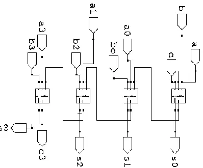
The Schematic of 2 – bit Vedic Multiplier design is shown in Figure 4.12. In the 2 bit Multiplier there are basically 2 half adder is used which is combinations of XOR Gate, AND gate is used and four AND Gate is used. In the 2-bit Vedic multiplier a0, b0, a1, b1 are the input of multiplier and s0, s1, c2, s2 are the output of Vedic Multiplier which is shown in
fig:-Figure 11: Schematic of 2 bit Vedic Multiplier
The Schematic of 4-bit Vedic Multiplier is shown in figure
IJIRT 100044
INTERNATONAL JOURNAL OF INNOVATIVE RESEARCH IN TECHNOLOGY17
Figure 13: Schematic of 4 – bit Vedic Multiplier using SERF AdderIJIRT 100044
INTERNATONAL JOURNAL OF INNOVATIVE RESEARCH IN TECHNOLOGY18
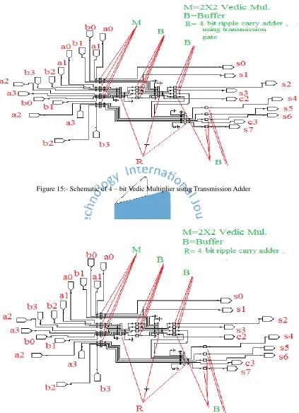
Figure 15:- Schematic of 4 – bit Vedic Multiplier using Transmission AdderFigure 16:- Schematic of 4 – bit Vedic Multiplier using 1-bit full Adder
IJIRT 100044
INTERNATONAL JOURNAL OF INNOVATIVE RESEARCH IN TECHNOLOGY19
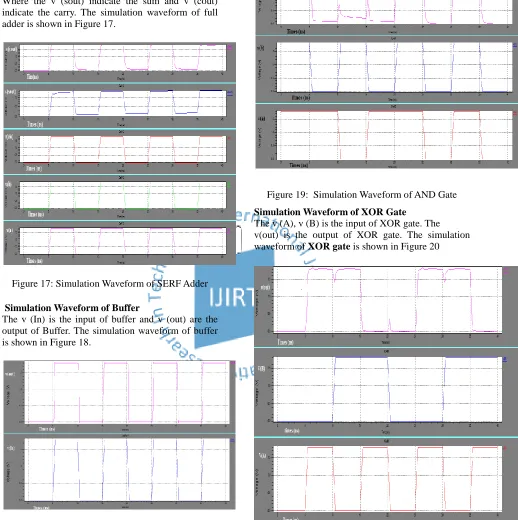
The v (a), v (b), v (cin), are the input of full adderand v (sout), v (cout) are the output of Full Adder. Where the v (sout) indicate the sum and v (cout) indicate the carry. The simulation waveform of full adder is shown in Figure 17.
Figure 17: Simulation Waveform of SERF Adder
Simulation Waveform of Buffer
The v (In) is the input of buffer and v (out) are the output of Buffer. Thesimulation waveform of buffer is shown in Figure 18.
Figure 18: Simulation Waveform of buffer
Figure 19: Simulation Waveform of AND Gate
Simulation Waveform of XOR Gate
The v (A), v (B) is the input of XOR gate. The v(out) is the output of XOR gate. The simulation waveform of XOR gate is shown in Figure 20
IJIRT 100044
INTERNATONAL JOURNAL OF INNOVATIVE RESEARCH IN TECHNOLOGY20
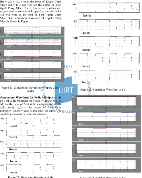
Simulations Waveform of Ripple Carry AdderThe v (a), v (b), v(c) is the input of Ripple Carry Adder and v (s1) and v(c) are the output of 4 bit Ripple Carry Adder. The v(c) is the carry which will be generated at the end of Ripple Carry Adder and v (s1) will work as the sum of 4-bit Ripple Carry Adder. The simulation waveform of Ripple Carry Adder is shown in Figure
Figure 21:-Simulations Waveform of Ripple Carry Adder
Simulations Waveform for Vedic Multiplier:- In the 2 bit Vedic multiplier the v (a0) ,v (a1)and v(b0),v (b1) are the input of 2-bit Vedic multiplier and v (s0), v(s1), v(s2), v(c2) is the output of 2-bit Vedic multiplier. Where v (c2) is indicates the carry. The simulations waveform is shown follows:-
Figure 22: Simulation Waveform of S0
Figure 23: Simulation Waveform of S1
IJIRT 100044
INTERNATONAL JOURNAL OF INNOVATIVE RESEARCH IN TECHNOLOGY21
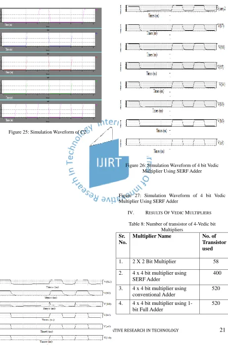
Figure 25: Simulation Waveform of C2Figure 26: Simulation Waveform of 4 bit Vedic Multiplier Using SERF Adder
Figure 27: Simulation Waveform of 4 bit Vedic Multiplier Using SERF Adder
IV. RESULTS OF VEDIC MULTIPLIERS
Table 8: Number of transistor of 4-Vedic bit Multipliers
Sr.
No.
Multiplier Name
No. of
Transistor
used
1.
2 X 2 Bit Multiplier
58
2.
4 x 4 bit multiplier using
SERF Adder
400
3.
4 x 4 bit multiplier using
conventional Adder
520
4.
4 x 4 bit multiplier using
1-bit Full Adder
IJIRT 100044
INTERNATONAL JOURNAL OF INNOVATIVE RESEARCH IN TECHNOLOGY22
5.
4 x 4 bit multiplier using
DPL Adder
616
6.
4 x 4 bit multiplier using
Transmissions gate Adder
445
Figure 28:- No. of transistor vs. Name of Multiplier
S1= 2x2 Vedic Multiplier.
S2 = 4 x 4 bit multiplier using SERF Adder. S3=4 x 4 bit multiplier using conventional Adder.
S4=4 x 4 bit multiplier using 1-bit Full Adder. S5=4 x 4 bit multiplier using DPL Adder.
S6=4 x 4 bit multiplier using Transmissions gate Adder.
Table 9: Power dissipations of 4-Vedic bit Multipliers
Sr.
No.
Multiplier Name
Power
Dissipations
At 500 MHz
1.
2 X 2 Bit Multiplier
0.21µw
2.
4 x 4 bit multiplier using
SERF Adder
2.11µw
3.
4 x 4 bit multiplier using
conventional Adder
9.55µw
4.
4 x 4 bit multiplier using
1-bit Full Adder
9.07µw
5.
4 x 4 bit multiplier using
DPL Adder
4.470µw
6.
4 x 4 bit multiplier using
Transmissions gate
Adder
0.3.11µw
Fig 29:-Average Power vs. Name of Multiplier
S1= 2x2 Vedic Multiplier.
S2 = 4 x 4 bit multiplier using SERF Adder. S3= 4 x 4 bit multiplier using conventional Adder. S4= 4 x 4 bit multiplier using 1 –bit full adder S5= 4 x 4 bit multiplier using DPL Adder.
S6=4 x4 bit multiplier using transmission gate adder.
Table 10: Propagations Delay of 4-Vedic bit Multiplier
Sr.
No.
Multiplier Name
Propagations
Delay
1.
2 X 2 Bit Multiplier
0.09ns
2.
4 x 4 bit multiplier using
SERF Adder
1.23ns
3.
4 x 4 bit multiplier using
conventional Adder
0.39ns
4.
4 x 4 bit multiplier using
1-bit Full Adder
1.45 ns
5.
4 x 4 bit multiplier using
DPL Adder
2.31ns
6.
4 x 4 bit multiplier using
Transmissions gate
Adder
IJIRT 100044
INTERNATONAL JOURNAL OF INNOVATIVE RESEARCH IN TECHNOLOGY23
Figure 30:- Delay vs. Name of MultiplierS1= 2x2 Vedic Multiplier.
S2 = 4 x 4 bit multiplier using SERF Adder. S3= 4 x 4 bit multiplier using conventional Adder. S4= 4 x 4 bit multiplier using 1 –bit full adder S5= 4 x 4 bit multiplier using DPL Adder.
S6=4 x4 bit multiplier using transmission gate adder.
V. CONCLUSION
This works focus on optimization of power and high performance of CMOS Vedic multiplier. The comparative analyses of Low power Vedic Multiplier using different adder logic style are done in this thesis. Result shows that the power consumed by the 2 bit Vedic multiplier is 0.21µw and the delay is 0.09ns. The average power consumed by the 4 bit Vedic multiplier using SERF Adder is 2.11µw and the delay 1.23ns. The power consumed by the 4 bit Vedic multiplier by using DPL Adder is 4.470µw and the 4 bit Vedic multiplier using DPL Adder is 2.31ns. The power consumed by the 4 bit Vedic multiplier by using transmission gate is 3.11µw and the delay is 3.01ns. The power consumed by the 4 bit Vedic multiplier using Conventional Adder is 9.55µw and the delay is 0.39ns. The power consumed by the 4 bit Vedic multiplier using 1-bit full Adder is 9.07µw and the delay is 1.45ns. Vedic Multiplier when used by using SERF adder is having lesser power dissipation.
VI. FUTURE SCOPE
Only one aspect of Vedic mathematics is touched in this work but there are so many other algorithms can be explored for multiplication. There is further scope
of improve implementation of the multiplier presented in this thesis to optimize the area & static power dissipations. Multiplication and divisions have innumerable application which can be implemented using Vedic mathematics. Floating point Vedic processor could be the extensions of this work.
REFERENCES
[1] K. Roy and S. C. Prasad, “Low-Power CMOS VLSI Circuit Design”, John Wiley & Sons, 1999. [2] A. P. Chandrakasan and W. Brodersen, “Minimizing Power Consumption in Digital CMOS Circuits”, Proceedings of the IEEE, vol. 83, no. 4, pp. 498-523, 1995.
[3] Shamim Akhter “Vhdl implementations of fast nxn multiplier based on Vedic mathematics” IEEE, 2007.
[4] Parth Mehta, Dhanashri Gawali “Conventional versus Vedic mathematical method for Hardware implementation of a multiplier” International Conference on Advances in Computing, Control, and Telecommunication Technologies, 2009.
[5] M.E.Paramasivam, Dr.R.S.Sabeenian “An Efficient Bit Reduction Binary Multiplication Algorithm using Vedic Methods” IEEE, 2010. [6] Asmita Haveliya “A Novel Design for High Speed Multiplier for Digital Signal Processing Applications” International Journal of Technology and Engineering System (IJTES), Vol2 .No1, 2011 [7] Manoranjan Pradhan, Rutuparna Panda, Sushanta Kumar Sahu “Speed Comparison of 16x16 Vedic Multipliers” International Journal of Computer Applications (0975 – 8887) Volume 21– No.6, 2011. [8] Prabir Saha, Arindam Banerjee, Partha Bhattacharyya, Anup Dandapat “High Speed ASIC Design of Complex Multiplier Using Vedic Mathematics” Proceeding of the 2011 IEEE Students' Technology Symposium, 2011.
[9] Pushpalata Verma, K. K. Mehta “Implementation of an Efficient Multiplier based on Vedic Mathematics Using EDA Tool” International Journal of Engineering and Advanced Technology (IJEAT) ISSN: 2249 – 8958, Volume-1, Issue-5,2011.
[10] V.Jayaparkash, S Vijayakumar, V.S. Kanchana Bhaaskaran,”Evealuation of the Conventional vs. Ancient Computations methodology for energy efficient arithemati architecture”, IEEE, 2011. [11] Sang-Mo Kang and Yusuf Leblebici, “CMOS
Digital Integrated Circuits”, Tata MCGRAW-HILL, Third Edition, 2003.
IJIRT 100044
INTERNATONAL JOURNAL OF INNOVATIVE RESEARCH IN TECHNOLOGY24
[13] D. Wang, M. Yang, W. Cheng, X. Guan, Z. Zhuand Y. Yang, “Novel Low Power Full Adder Cells in 180nm CMOS Technology”, Industrial Electronics and Applications, 4th IEEE Conference on Digital Object Identifier, pp. 430-433, 2009.
[14] Neil H.E. Weste, “CMOS VLSI Design”, Pearson Education Asia, Third Edition, 2006.
[15] C.J. Nicol, P. Larsson, “Low Power Multiplication for FIR Filtering,” Bell laboratories, Lucent Technologies, Holmdel, NJ 07733.
[16] R. Fried, “Minimizing Energy Dissipation in High-Speed Multipliers,” International Symposium on Low Power Electronics and Design, pp. 214-219, 1997.
[17] Shivshankar Mishra, V. Narendar, Dr. R. A. Mishra, “On the Design of High-Performance CMOS 1-bit Full Adder Circuits”, International Conference on VLSI, Communication & Instrumentation (ICVCI), IEEE Proceedings Published by International Journal of Computer Applications, pp.1-4, 2011.
[18] P. G. Parate, P. S. Patil and S. Subbaraman, “ASIC Implementation of 4 Bit Multipliers”, First International Conference on Emerging Trends in Engineering and Technology, IEEE, pp. 408-413, 2009.
[19] P. C. H. Meier, “Analysis and Design of Low Power Digital Multipliers”, Ph.D. Thesis, Carnegie Mellon University, Department of Electrical and Computer Engineering, Pittsburgh, Pennsylvania, 1999.