Design and Implementation of Multi-Rate
Encryption Unit Based on Customized AES
Ashraf D. Elbayoumy, Haitham Eldemerdash
Egyptian Armed Forces
Email:
[email protected]
Abstract — The demand for security in wireless
communication channels is rapidly growing. In this exertion a proposed encryption unit which adopts the AES (Advanced Encryption Standard) as the encryption algorithm is presented. In previous work a customized version of the “AES” block cipher to suit proprietary data encryption applications is introduced [1]. In this paper, a hardware implementation of the algorithm, using Field Programmable Gate Arrays (FPGA) is presented. Furthermore, the structure of Encryption unit, the implemented micro-architecture, the simulation, and implementation results will be discussed. In addition, the detailed description of the various micro-architecture modules is included.
Index Terms — Advanced Encryption Standard (AES), Field
programmable gate arrays (FPGA), Very high speed integrated circuit Hardware Description Language (VHDL), Micro-Architecture, Encryption, and Algorithm.
I. INTRODUCTION
T
he AES algorithm can be efficiently implemented byhardware and software [2], [3]. Software implementations cost the smallest resources, but they offer only limited physical security. Because of the growing requirements for high-speed, high-volume secure communications combined with physical security, hardware implementation of cryptography takes place. Customizing the AES algorithm attracted attention of researchers to provide proprietary security. Moreover, the proposed customized AES is incorporated in an encryption unit that is implemented using FPGA. The customization of the AES is designed to cover three main AES cryptographic functions, these are: S-box Generation, Mix Column Transformation, and Key Expansion Function. The S-Box generation process results in a new S-Box. The new S-Box is tested to be sure of satisfying the required cryptographic features: algebraic degree, non linearity, propagation criteria, correlation immunity, and balancedness. The customized AES is tested also against statistical randomness properties [1]. Using FPGA, the architecture of the encryption unit is composed of two main units. The first unit is the Proposed Encryption Unit which divided into four main functional block, these are the loop controller module, the encryption and decryption round module, key expansion function module, and the ram module. The second unit is Multi-Rate Unit which composed of four main modules UART module, Clock divider module, Signal Compression module, and Decision module. In the next sections the Multi-rate Encryption unit structure and performance testing the building blocks of the
architecture of the encryption unit will be discussed. Also the details of the simulation results are provided.
II.FPGADESIGN ARCHITECTURE
A. FPGA Design Architecture for Proposed Encryption Unit
In this section, a detailed description of the proposed FPGA architecture for the Customized AES Algorithm is provided [4], [5]. The design consists of four main units; the first unit is loop controller module which responsible for controlling the encryption and decryption processes by receiving an external interrupt and mode select signals which are used to control the data processing during the round operations in the second module, the second unit is AES Encryption & Decryption Round module this module performs the encryption and decryption operations during round functions by receiving data, round keys, and control signals from other modules. It consists of four main components, four mix column units to perform mix column function, 32 Rom units which contain S-box and inverse S-S-box values. Four inverse mix column units to perform inverse operation of mix column function and the last component is add _round _key to make XOR operation of data and round key.
Figure 1Top Level of a Customized Unit
seed key (128 bits) based on the AES key expansion algorithm. It produces a linear array of 44 words (176 bytes) [8] by expanding the four words (16 bytes) key input. Key Expansion Function module consists of three components, the key controller unit which is used for fully controlling the round keys generation function, 4 units of Rom unit which contain S-box values, the third component is Rcon unit which used to make XOR operation between round constant and substituted word. The last main unit is Ram module; it is responsible for generating the output sequence of (128) output round key. All the four basic units are illustrated in Figure 1. All modules are designed using VHDL design Entry .The used tools is FPGA advantage 5.2 from Mentor Graphics [9]. In the following subsections every module will be described in details.
A.1 Loop controller module
In this module both 128-bit of AES input data and round key data are saved into internal round register. The controller module must receive control signals to start operate; this signals are the incoming data interrupt which comes with input data. Mode select signal to mange between encryption and decryption process called (enc_dec), (key_rdy) signal to confirm that the key expansion process was completed and the desired key are ready to use, round ready signal to determine that the round functions was finished and give the round output data (128 bits) as shown in Figure 2.the module responsible also to generate control signals to the next module such as mix column Function activation to control its status during the last round , key interrupt signal for adding a new round key, round address and round interrupt signal to control the round processing.
Figure 2 The AES loop controller module
A.2 AES encrypt decrypt round module
The Encryption/Decryption module consists of four main components, four mix column units to perform mix column function by receiving (mixcol_activation) signal as shown in Figure 3 to perform this function for whole rounds except the last round, 32 units of Rom unit which contain S-box and inverse S-box values. Four inv mix column units to perform inverse operation of mix column function and the last unit is add round key to make XOR operation between data and
round key, and this module also applies shift row function
with its inverse operation to the data entry. Finally when all of
these operations completed the module generates a round output with 128-bits and control signal called round output ready.
Figure 3 AES encrypt decrypt round module
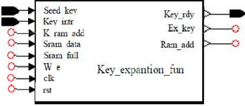
A.3 Key expansion function module
The Key expansion function module consists of three main components, the key controller unit which used for fully control the round keys generation function and internal S-box processing by generating and control a memory addressees as Figure 4 and also make Rotate Word function as a one-byte circular left shift on a word. The result after both functions rotation and substitution word is XORed with a round constant in the second component the Rcon unit.
Figure 4 key expansion function module
A.4 Ram_11x128 bits module
This module was written by standard (RAM) memory structure in (VHDL) coding for saving the hardware resources. There are control signals to mange read/write process as w_e, address control signals which receive the ram address from the key expansion function and data input bus (128 bits) which registers the expanded key from the key expansion module as shown in Figure 5.
Figure 5 Ram_11x128 bits module
(128 bits) which is important for two other modules which is AES loop controller module and encrypt decrypt round module.
B. FPGA Design Architecture for Multi-Rate Unit
The multi rate module responsible for dealing with three different bit rates 600, 1200 and 2400 bps in transmission or reception process form/to serial data port and convert this variable bit rates from serial port to the standard FPGA clock board speed which is 50 Mbps for Spartan-3A/3AN FPGA starter kit board which used for downloading our design [8]. This unit was designed in 10 modules which will be explained in next sections see Figure 6. The fist three modules are UART modules which are receive or transmit 128 bits input data from/to serial ports. The second three modules are frequency divider modules which are responsible for converting three variable bit rates to desired clock. The third three modules are signal compression modules which used for compressed the interrupt signals which comes from UART modules and decision module to be adapted with 50 Mbps. the fourth module are decision module which decide which UART module will be operate according to selected data rate.
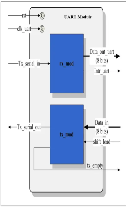
B.1 UART module
A UART is a Universal Asynchronous Receiver Transmitter device which utilizes an RS232 serial protocol and is used in all personal computers to provide the interface between the CPU and the serial port [9].
This module is responsible for interfacing with the serial port RS-232 on the FPGA Board to communicate through it with the serial port in the computer (data source); on the other hand it is used to send the serial data to the multi rate unit through the Tx serial port.
A typical UART consists of a transmitter partition and a receiver partition as shown in Figure 7 the UART consists from two sub modules rx_mod and tx_mod modules. As shown in Figure 6, Serial data input (Sin) signal loads an eight bit word into the UART module. The UART (tx_mod) frames the word with a START bit (logic '0') at the beginning, and a STOP bit (logic 'l') at the end of the word and sends the framing information along with the data in a serial manner from the Least Significant data Bit (LSB) to the Most Significant Bit (MSB). The reverse operation is done in the receiving by removing the START bit and the STOP bit by the rx_mod module and collecting the data in the output port (Sout) accompanied with the interrupt.
From PC F re q _ d iv _ 3 UART_1
UART_2
UART_3 G G RST CLK F re q _ d iv _ 2 F re q _ d iv _ 1 Sig_comp_1 Sig_comp_2 Sig_comp_3D
ec
id
e
m
o
d
u
le
S er ia l d at a I/ P To PC F ro m R es et S w it ch F ro m C lo ck S o u rc e Intr_uart_out2 Intr_uart_out3 Intr_uart1 Intr_uart2 Intr_uart3 Clkuart_out1 Clkuart_out2 Clkuart_out3Decision (0, 0)
Dout_uart3 Dout_uart2 Dout_uart1 Data_in_uart3 From Top Data_in_uart2 Data_in_uart1 S er ia l d at a O /P Intr_uart_out1
The implemented UART is operated without parity, eight data bits and one stop bit. The clock speed is adjustable depending on the input clock to the UART module (clk_uart), in the proposed system the serial port speed is 600, 1200 and 2400 bps hence the clk_uart will be change according selected data rate that is why we design three UART modules. The tx_empty signal is for indication that the tx_mod has finished transmitting the byte on the data_in port and ready to accept new data to transmit. The rx_mod and tx_mod modules are described in VHDL.
Figure 7 UART module internal structure
B.2 Clock divider module
As shown in Figure 6, the clk_divider module inputs are two main signals (clk , rst), while it has one output which is new clock signal called clk_uart. This module is responsible for generating the UART needed clock for its operation as the UART has specific baud rates must operate with (600, 1200 and 2400), and usually these frequencies will not be available on the FPGA board clock sources, therefore there will be a need for generating them by dividing the available clock source. In the proposed system, the main clock source available on the FPGA board equals to 50 MHz hence the dividing value will be change to get the needed data rate.
B.3 Signal Compression module
The Signal Compression module responsible for generating interrupt signals with master clock board 50 Mbps to be adapted with decision module clock. the Signal Compression module inputs are clk, rst, and intr_uart_out (output interrupt from UART module), while it has one output which is intr_uart., hence we have 3 sig_comp modules to deal with 3 UART modules with different clock and one sig_comp module connected with decision module. As shown in Figure 6.
B.4 Decision module
The Decision module inputs are three UART interrupts (intr_uart1, intr_uart2, and intr_uart3) coming from Signal Compression module that initiate data bus generating from UART modules to Decision module, while it has two outputs decision signal which select between 3 UART modules according to selected data rate this done by checking on the received pattern coming in data out from UART module and comparing this data with Preamble data (2E12AB34CD56) to detect the modification happened with data rate. Hence if we received this preamble data from any of UART modules we can know which one is working at this moment and also which data rate was selected. Table 1 indicates the relation between decision signal combinations and selected data rate.
Table 1 decision signal combinations
Data rates (bps) decision signal
600 (1,0)
1200 (0,1)
2400 (1,1)
IV.SIMULATION
A. Customized AES Encryption unit simulation
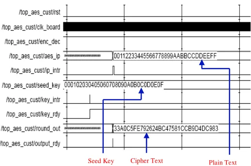
The simulation result of the top design of customized AES encryption unit is shown in Figure 8. The data with length of 128-bit is received on port (aes_ip) in AES controller module and then encrypted using the (seed_key) with its sub rounds keys to get the ciphered data output 128-bit denoted as (round_out). The Figure shows the five main control signals produced by the loop controller module and key controller module. The enc_dec signal is used for mode selection between encryption and decryption process, both (ip_intr) and (key_intr) interrupt signals are used to apply input data and seed key data, (key_rdy) and (output_rdy) that give the information that both key generation in key expansion function and encryption operation are completed.
Figure 8 Timing diagram of encryption process
Figure 9, shows the simulation waveforms for decryption process to be confirm that the plain data will be recovered again from ciphered data. From simulation results we find that the key expansion process finished and generated all round keys in (112 m sec) and also the encryption process take (8300 n sec) till the cipher output is ready. For decryption process, the overall operation takes (20200 n sec) [1]. The clock speed used is 50 MHz this mean that the design clock duration is 20 n sec. From Figure 9 we observe that the value of enc_dec control signal changed according to the process selection between encryption and decryption operations.
Figure 9 Timing diagram of decryption process
B. Multi rate unit simulation
The simulation results of the test bench illustrated in Figure 10 will be discussed for the Multi rate unit by tracking the data flow inside it. The UART_Tx and UART_Rx module read the serial data with name dout_uart1 then transmits these data serially through the serial port to the customized AES
unit. The clk and rst signals are also generated with appropriate rates needed to simulate the real case. The data enter the multi_rate unit serially through Sin port to be converted to bytes removing the start and stop bits according to the RS-232 protocol by the UART_Rx reception module on the dout_uart port accompanied with an interrupt on intr_uart_out1 port as shown in Figure 10.
Figure 10 Timing diagram of multi-rate unit
The decide module comparing the received data with the preamble sequence (2E12AB34CD56) to detect the change of bit rate and generate decision signal as shown in Figure 11 related to selected data rate.
Figure 11 Timing diagram of UART
In Tx mode UART_Tx module takes 10 bits for transmission 8 bits containing serial data entry as (2A) shown in Figure 11 and 1 bit as start and 1 bit as stop. The Tx empty signal called xmitmt and shift_load signal changed together with rising edge of the clock to indicate that transmission process was finished and waiting new serial data. When decision signal changed, init signal was generated to erase all saved data in
Plain Text
Seed Key Cipher Text
Cipher Text
Seed Key Plain Text
Preamble sequence Decision Signal
Empty Signal UART I/P Data
Cust AES unit and make it clear to received a new serial I/P with new data rate.
III.HARDWARE TEST
A. Testing procedures
To begin the testing procedure, the design must pass through the synthesis, place and route, and downloading phases. These steps are the basic steps needed to translate the VHDL code describing any system into a real hardware depending on the available resources (tools, FPGA chips).
The design synthesis and downloading procedures is carried out using Xilinx software ISE 9.1i on the FPGA board Spartan-3 Micromodule that contains Xilinx Spartan-3A/3AN FPGA XC3S700AN-4FG484 [8] and Xilinx Platform-Flash XC2C256. After the synthesis step is done the user define the inputs and outputs ports locations in the user constrains file (ucf) before the Place and Route step to identify the data entrance into the designed system and the data capturing method after the processing is done. Then the design completes the downloading sequence as recommended by Xilinx Vendor of Project Navigator ISE, Release 9.1i.
The synthesis results and reports will be introduced first then the hardware testing procedure and results will be discussed.
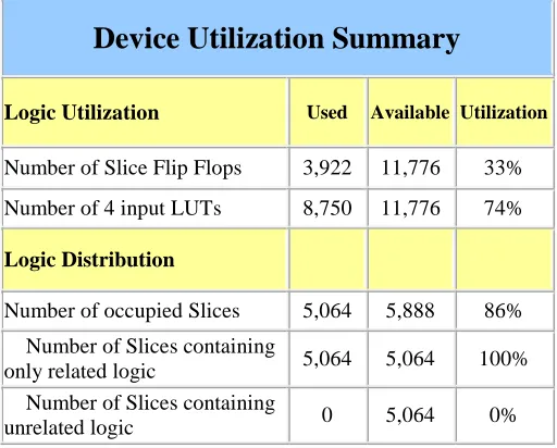
Table 2 illustrates the device utilization report generated from the ISE 9.1i software describing the percentage of chosen chip XC3S700AN-4FG484 occupied by the Multi-rate Encryption unit and as noticed from this table that the transmitter unit didn't occupy more than 86 % from any of the chip resources.
Table 2 Utilization summary for the Multi-rate Encryption unit
Device Utilization Summary
Logic Utilization Used Available Utilization
Number of Slice Flip Flops 3,922 11,776 33%
Number of 4 input LUTs 8,750 11,776 74%
Logic Distribution
Number of occupied Slices 5,064 5,888 86%
Number of Slices containing
only related logic 5,064 5,064 100%
Number of Slices containing
unrelated logic 0 5,064 0%
Total Number of 4 input
LUTs 8,849 11,776 75%
Number used as logic 8,750
Number used as a route-thru 99
Number of bonded IOBs 19 372 5%
IOB Flip Flops 2
Number of GCLKs 4 24 16%
Number of RAMB16BWEs 4 20 20%
Total equivalent gate count
for design 98,271
Additional JTAG gate count for
IOBs 912
B. Hardware setup and results
The main objective of the hardware test is testing the designed system after downloading to make sure that the downloaded hardware function properly and its results are identical to the simulation results. The setup is as illustrated in Figure 12; the computer is the data source and the data destination according to the selected operation between encryption and decryption. The computer and Multi-rate unit are connected serially via RS-232 as shown in Figure 12. The switch (SW0) in FPGA board must be put in position logic "1" or "0" according to required operation "Encryption" or "Decryption" respectively. The data is sent from computer to the Multi-rate unit which receives the data through the serial port then applies customized encryption algorithm processes to received data, then it retransmit the resulted data again to the computer through a serial connection.
Figure 12 Testing setup connection
Special software is developed to test the transmission and reception by sending and receiving data through the serial port (RS-232) using the Visual Basic 6 programming language. The software interface is illustrated in Figure 13. It simply works by adjusting the port setting then writing the data in the text box found in the Send Data panel and finally pressing the send button. The reception part is done automatically after pressing the Receive data button in the Receive Data panel. The received data is displayed in the text, HEX, ASCII, and
Computer
Serial Port RS-232
Multi-rate Encryption Unit
binary formats also the sent data can be written in text, HEX, ASCII, and binary formats.
Figure 13 The Software interface
After several trials of sending and receiving data frames to and from the computer and Multi-rate unit and comparing the results with the simulation outputs illustrated previously to be sure of the correct functioning of the downloaded system. It was clear of that the downloaded design operates correctly in encryption and decryption operation with different bit rates after applying the customized encryption unit.
V.CONCLUSION
This paper provides a detailed description of a hardware implementation for proposed multi-rate encryption unit using FPGA technology. It goes into more details in the design of the building blocks of the architecture of this unit. And also provide the details of the simulation results and hardware testing. All the main system components are described in VHDL. All interfaces and interconnect modules used for interfacing, processing and controlling are described in
VHDL.
REFERENCES
[1] N.Hamdy, K.Shehata, H.El-demerdash. “Design and Implementation of Encryption Unit Based on Customized AES Algorithm” IJVIPNS International Journal of Video & Image Processing and Network Security, Vol: 11 No: 01, February 2011.
[2] National Institute of Standards and Technology (NIST),
Advanced Encryption Standard (AES), Federal
Information Processing Standards Publications (FIPS) PUBS #197, 2001.
[3] J. Daemen, V. Rijmen, AES proposal: Rijndael Document version 2, 1999.
[4] Douglas L. Perry, "VHDL: Programming by Example", Fourth Edition, 2002.
[5] Volnei A. Pedroni, “Circuit Design with VHDL” Fourth Edition, 2004.
[6] William Stallings, "Cryptography and Network Security Principles and Practices", Fourth Edition, 2005.
[7] Clive “Max” Maxfield, “The Design Warrior’s Guide to FPGAs” 2004.
[8] Spartan-3A/3AN FPGA Starter Kit Board User Guide UG334 (v1.1) June 19, 2008
[9] Ben Cohen, “VHDL Coding Styles And Methodologies”, Kluwer Academic publishers, United States, 1995.