e-ISSN: 2278-067X, p-ISSN: 2278-800X, www.ijerd.com
Volume 11, Issue 12 (December 2015), PP.01-09
Synchronous Micro pipelined 32-Bit Multiplier
Using Hybrid Array
Priya Barange, Sunil Malviya, Paresh Rawat, Saima Ayub
Department of Electronics and Communication Engineering TCST, Bhopal, (MP), India
Abstract:- In this paper, design of two different multipliers are presented, one by introducing Carry Select Adder (CSLA) in partial product lines and another by synchronous Micro pipeline multiplier. The multipliers presented in this paper were all modelled using Very High Speed Integration Hardware Description Language. The design employs the modified Booth algorithm. A 2-phase micro-pipelined latch controller is used which controls the 4-phase pipeline with standard transparent latches. The comparison is done on the basis of three performance parameters i.e. Area, Speed and Power consumption. Previously in the literature, performance analysis was carried out between multiplier.
Keywords:-Multiplier, Carry Select Adder, pipelining, synchronous clock, VHDL modelling, Xilinx14.4.
I.
INTRODUCTION
Synchronous pipeline multiplier has some important advantages such as increased computational ability, reduced dynamic power dissipation, increased data-density, Therefore with the help of synchronous pipeline multiplier we have designed synchronous pipeline multiplier architecture. The performance of multiplier architecture is compared based on Carry select Adder [7] based Multiplier and Micro-pipelined [14] based multiplier.
In many practical application such as arithmetic processor, FIR filter, digital signal processing, multiplier plays important role. In digital system, the performance is basically estimated by the performance of the multiplier. Many researchers with progress in technology have endeavored to implement the multipliers which offer high speed, low power consumption, regularity of layouts. The Arithmetic processors represent important example, where multi-valued data representation provides additional theoretical and design flexibility.
Alternatively, for the multi- valued [1][5] representation, the system represents the multi-valued segments,
which in turns it may have the binary parts.
In VLSI design, researchers mainly concentrate on speed, power dissipation and area. The kinds of high speed multipliers are Parallel-multiplier [11], Booth multiplier, Braun-multiplier. In the conventional type multiplier, the numbers of partial products to be added are determined by number of bits, the multiplier or multiplicand are being used. While the number of bits in the multiplicand or the multiplier increases, the longer time it takes to produce the product. Digital multiplication is the processes where two binary numbers, the multiplier and multiplicand are integrate into the result forming a series of bit-shift and bit-additions algorithm. There are different type multipliers obtainable depending upon the implementation in which they are used.
Conventional array multiplier is based on efficient full adder in which the multiplication is obtained by the
partial product method. In digital system, an array multiplier [8] includes the parallel multiplication, is done in the following three steps:
1. Initiation of the partial product bits.
2. The collection of partial product bits into two rows. 3. The computation of endmost product using a Full adder.
The multiplicand and multiplier of partial product bits are produced by partial product generation. Partial product depletion is used to shorten the partial product bits. In Multiplication, product of two bits produces the output which results twice than that of the real bit. For the reduction of area costs, it is needed to shorten the partial-product bits to the necessitate precision. This paper is organized as first part consists of basic circuit design of quaternary logic which is used to implement multiplier. Second part is based on the designing of multiplier architecture. Third part is based on the examination of multiplier design & conclusion.
Suppose the register size for product be 64 bits and the registers size of multiplicand is 32 bits. Save the multiplier in the least-significant half of the product register then Clear the most significant half of the product register. Repeat for 32 times, the following steps:
1. If the least significant bit of the product registers is one then add the multiplicand to the most-significant half of the product registers.
3. Shift-in, carry bit into the most significant bit of product register. Figure 1 shows block diagram for such type of multiplier. Multiplicand Shift right Multiplier
Figure 1 Multiplier of two n-bit values
II.
PIPELINE
OPERATION
Pipeline operation: A key attribute of this pipeline is unlike all synchronous latch-based pipelines, the latches are generally transparent that is data passes directly through them. Therefore, initially the whole pipeline forms a flow through the combinational route. Basically, after the data progresses through the individual stages of latches, the transition on the control input makes these latches be opaque; thereby the protecting and storing the data from some further changes on the stages input media.
Once the data advances through the upcoming stages of latches, the transition on the control input, communicated from the next stage, makes the present stages of latches transparent, thus it safely allowing the next data item to enter.
1. Important characteristic of array multipliers is to allow the Pipelining process. 2. The long-term delay of carry-propagating addition must be minimized.
3. Achieved by replacing CPA with several additional rows allow the carry-propagation of only one position between the consecutive rows.
4. To support pipelining all cells must include latches, each row handles a discrete multiplier and multiplicand pair. Registers are needed to propagate multiplier bits to their destination, and then propagate completed product bits.
III.
PIPELINED
HANDSHAKE
ARRAY
MULTIPLIER
Array multipliers [15][12] and tree multipliers are rather fast but, or hardware hungry. Serial multipliers need less area but have a very low throughput. The Iterative multipliers are better choice in considering the tradeoff between the silicon area and speed. The synchronous circuit, which is based on four- phase handshaking protocol, cans simply uses the transparent latches in the form of pipeline without two-to-four phase signaling converters. While the two-phase hand-shaking protocol is faster and costs the low power because it eliminates the redundant return-to-zero transitions. The determination of commissioning the hybrid hand-shaking protocol is combines the benefits of both four-phase protocol and two-phase protocol.
With pipelining [14] techniques used, there are iterative multipliers can obtain an equal throughput as similar of parallel multipliers if we ignore the delay of registers or latches. The multiplier of uses a synchronous pipeline structure clocked by an inverter oscillator. Compared to synchronous pipeline, the self-timed pipeline has the main advantages is higher speed: synchronous pipeline method uses handshaking protocol and its operating speed is determined by definite combinational logic block remission of each stage rather than the analytic delay of all stages. Less silicon area: Standard transparent latches are used in synchronous pipeline whereas synchronous pipeline must employ the edge-trigged registers to hold the stages. The Edge-trigged
registers occupy the double silicon space a
s
compared to transparent latches. Furthermore, transparent latchesare twice times faster than edge-trigged registers, which further self-timed the pipeline’s advantage in high speed.
Mn-1 M0
n- Bit Adder Shift and Add Control Logic
An-1 A0 AA A0
IV.
MICROPIPELINE
MULTIPLIER
ARCHITECTURE
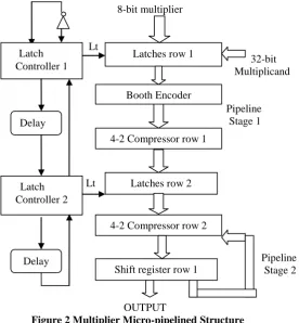
Basic multiplication can be realized by the shift adder algorithm by generating partial products and adding successive then properly shifts the partial products. Thus, the multiplication is directly proportional to the number of partial products to be added. In all multiplier circuits, two types of adders are present. They are full adder and half adder. The multiplier designed in this paper, uses the modified booth algorithm method and supports 32-bit integer multiplication for both signed and unsigned operands. The multiplier architecture is shown in Figure 2. This is a two-stage synchronous pipeline structure using bundled-data protocol. In synchronous the bit-sleep is negligible bit-sleep error is also called data miscommunication error because data error chances are minimum. The first stage includes a booth encoder; a pipeline latches row and a four-to-two compressors row. The second stage including a pipeline latches row, a four to two compressors row and a shift registers row. 8-bit multiplier Lt 32-bit Multiplicand Pipeline Stage 1 Lt Pipeline Stage 2 OUTPUT
Figure 2 Multiplier Micro-pipelined Structure
The booth MUX: The booth multiplier is composed of 4 transmission gates. With elegant control signals, the Booth MUX can minimize the short circuit currents for low power reasons. Figure3 shows the Booth MUX (BOOTH MLTIPLEXER)
Figure 3 the booth MUX
V.
CARRY
SECLECT
ADDER
BASED
MULTIPLIER
The select adder [8][10] is straightforward however rather quick. As shown in figure 4; the carry-select adder typically consists of two ripple carry adders and an electronic device. Adding two n-bit numbers with a carry-select adder is finished with two adders (therefore two ripple carry adders) so as to perform the
Mi
+2* −2* −1* +1*
Outi
+1 −1 +2 −2 0
Mi+1
Latches row 1
Booth Encoder
4-2 Compressor row 1
Latches row 2
4-2 Compressor row 2
Shift register row 1
A3/B3 A2/B2 A1/B1 A0/B0
FA FA FA FA
Cout
FA FA FA FA
Cin
S3 S2 S1 S0 Figure 4 Computation diagram of Carry Select Adder
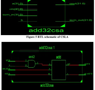
Figure 5 RTL schematic of CSLA
Figure 6 RTL schematic of implemented CSLA
In Carry select adder scheme, blocks of bits are added in two different ways: First by assuming a carry-in of bit- 0 and the Second with a carry-carry-in of bit- 1.This results carry-in two pre-computed carry-out and sum signal pairs (s0i-1: k, c0i; s1i-1: k, c1i), later the block’s real carry-in (ck) becomes known and the correct signal pairs are then selected. Basically, multiplexers are used to propagate carries.
In CSLA (Carry select adder), because of multiplexers larger area is needed. And as comparisons with Ripple Carry adder, carry select adder have less delay Hence we always take the Carry Select Adder as working with the smaller number of bits.
Logic equations: si-1: k = ck s0i-1: k + ck s1i-1: k ci = ck c0i + ck c1i
C0
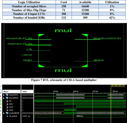
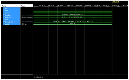
Figure 5 and Figure 6 shows the RTL schematic diagram of CSLA Adder based multiplier. Hence from figure 7 and figure8, the implemented CSLA multiplier is design which shows the output in the form of clock representation in which the product of multiplier and multiplicand simulation waveform is carried out. Table 1 show the device utilization summary which is used to implement the CSLA based 32-bit multiplier.
Table 1 Device utilization summary (estimated values) of CSLA based multiplier
Logic Utilization Used Available Utilization
Number of occupied Slices 198 16640 1%
Number of Slice Flip Flops 71 33280 0%
Number of 4 input LUTs 308 33280 0%
Number of bonded IOBs 132 309 42%
Figure 7 RTL schematic of CSLA based multiplier
Figure 8 Clock representation of CSLA based 32-bit multiplier
VI.
MICROPIPELINED
MULTIPLIER
Serial multiplication is the process of data processing of the partial product and summing the partial product together. Quaternary ripple carry adder based multiplier consists of multiplicand Shift-in Shift-out shift register, multiplier Shift-in Shift-out (SISO) shift register, and product. The speed of operation of serial multiplier is slow because of operand entering serially. In carry adder based multiplier, the partial product
accumulation operation is serial, because after n iterations final product is obtainable where’ n’ is the maximum
number of digits in each operand.
the partial product and the partial product is then stored in partial product register and partial product shift register shifts the partial product after every clock cycle.
Multiplier structure is then implemented with carry select- adder as shown in Fig 8 .Then the comparative analysis and Simulation results of micro pipelined based 32-bit multiplier & carry select adder based 32-bit multiplier simulation results waveform is carried out which is shown in figure 8 and figure 10.
The micro-pipelined[12]multiplier is design synchronously which uses global clock which controls the data flow in the data path. The RTL schematic diagram of micro-pipelined based multiplier is shown in Figure 9.
Table 2 Device utilization summary (estimated values) of micro-pipelined multiplier
Logic Utilization Used Available Utilization
Number of occupied Slices 121 16,640 1%
Number used as Flip Flops 47
Number used as Latches 37
Number of 4 input LUTs 185 33,280 1%
Total Number Slice Registers 84 33,280 1%
Figure 9 RTL schematic of micro-pipelined multiplier
The clock implementation of the implemented micro-pipelined based multiplier is shown in figure 10 and Table 2 show the device utilization summary which is used to implement the micro-pipelined based 32-bit multiplier.
VII.
RESULTS
&
CONCLUSION
In this Section, the results obtained from the Synthesis and Simulations reports are presented. Here we are proposed the comparison between Synchronous micro-pipelined based 32-bit multiplier architecture and CLSA based 32-bit multiplier pipelined multiplier in terms of power, area and time. The micro-pipelined multiplier circuits have low dynamic power dissipation features and improved the time performance. The micro-pipelined multiplier circuits have low dynamic power dissipation features and improved the time performance
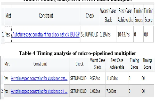
Table 3 Timing analysis of CSLA based multiplier
Table 4 Timing analysis of micro-pipelined multiplier
Table 3 and Table 4 are the snapshots of the timing constraints results and Table 5 and Table 6 are the snapshots of Supply Power results are taken from the Xilinx (14.4) software, Synthesis tool XST (VHDL/VERILOG) family SPARTAN-3A DSP. Table 3 and Table 4 show the performance of timing analysis in which auto time for net clock whose best case achievable time with no errors for CSLA based multiplier is 10.437ns and for micro-pipelined based multiplier is 7.686ns.
Table 5 Power analysis of CSLA based multiplier
Table 5 and Table 6 show the performance of power analysis in which total power used for CSLA based multiplier is 0.123w and total power used for micro-pipelined based multiplier is 0.121w. The total power is evaluated by using the general formula:
Power (Watt) = Voltage (Volt) × Current (Ampere)
Hence to calculate the power dissipation the general equation is expressed as: P = f × Ceff × V2dd
Where, f is the switching frequency, Ceff is the effective capacitance, the average capacitance (dis)charged in
one cycle and Vdd is the supply voltage.
From the area analysis graph as shown on Figure 11, it is concluded that as compared to CSLA[7][8][9] based multiplier, micro-pipelined[15] multiplier is fast in speed performance and it gives low power consumption and less area required. This type of multiplier can be used for the design of ALU (Arithmetic Logical unit). The analysis result is concluded on the basis of Table 1 and Table 2 which shows that area required for CSLA based multiplier is more than the area required for micro-pipelined based multiplier. Area Analysis is defined as:
Area (aout) = number of LUTs i.e Logic units (bluts) used + number of occupied slices(bsl).
Area Occupied for CSLA based multiplier: aout = bluts+ bsl
aout =308+198
aout =506
Area Occupied for Micro-pipelined based multiplier: aout = bluts+ bsl
aout =185+121
aout =306
Figure11 Area Analysis chart of CSLA and micro-pipelined based multiplier
From all this analysis it is found that less area required therefore low power consumption because area reduction is directly proportional to Power and inversely proportional to high efficiency. Furthermore, this
multiplier is more robustbecause the handshaking protocol can match the exact latency of each pipeline stage.
REFERENCES
[1]. K. C. Smith, “Multiple-valued logic: a tutorial and appreciation,” IEEE Computer, vol.21, April 1988.
[2]. Ricardo Cunha, Henri Boudinov and Luigi Carro “Quaternary Look-up Tables Using Voltage-Mode CMOS Logic Design” Proceedings of the 37th International Symposium on Multiple-Valued Logic (ISMVL'07), 13-16 May, 2007.
[3]. Ricardo Cunha G. da Silva , “A Novel Voltage Mode CMOS Quaternary Logic Design” , IEEE Transactions on Electron Devices , vol.53, no. 6 , June 2006.
[4]. Satyendra R.P.RajuDatla, Mitchell A. Thornton Quaternary Voltage-Mode Logic Cells and Fixed-Point Multiplication Circuits ISMVL.2010.
[5]. J.T. Butler, (editor), Multiple-Valued Logic in VLSI Design, IEEE Computer Society Press, 1991.
[6]. Z. Navabi, VHDL Modular Design and Synthesis of Cores and systems, 3rd ed., McGraw-Hill Professional, USA, 2007. ISBN: 9780071508926.
[7]. V.Vijayalakshmil, R.seshadri, Dr. S. Ramakrishnan , “Design and Implementation of 32 Bit Unsigned Multiplier Using CLAA and CSLA”,978-1-4673-5301-4/13/$31.00 @2013 IEEE.
[9]. Hasan Krad and Aws Yousi( "Design and Implementation of a Fast Unsigned 32-bit Multiplier Using VHDL", 2010.
[10]. Rajender Kumar, Sandeep Dahiya, “Performance Analysis of Different Bit Carry Look Ahead Adder Using VHDL Environment, International Journalof Engineering Science and Innovative Technology (IJESIT)”, Volume 2, Issue 4, July 2013.
[11]. Vrushali Gaikwad, Rajeshree Btramankar, Amiruna warambhe“32 bit parallel multiplier using VHDL ”International Journal of Engineering Trends and Technology (IJETT)”, Volume 9, Issue 3, March 2014.
[12]. R. B. Reese, M. A. Thornton, and C. Traver, “Two-phase micropipeline control wrap with early evaluation,” Electreonic Letters Online no. 20040256, IEE, no. 3, 2004.
[13]. F. K. Gurkaynak et al., “Gals at eth zurich: Success of failure?” in Proc. of the 12th IEEE International Symposium on Asynchronous Circuits and Systems, 2006, pp. 150–159.
[14]. Tyanev, D., Popova, S., 2011. “Branch management into micropipeline joint dot”, Applied Technologies and Innovations, Vol.5, pp.11