Improving the efficiency of PV Generation System Using
Soft-Switching Boost Converter with SARC
Krishna Enugala
1, M.Sridhar
2, K.Prasad Yadav
31,2
M.Tech,SCCE,KNR
3Asst.Professor,SCCE
Abstract—In order to improve the efficiency of energy con-version for a photovoltaic (PV) system, a soft-switching boost converter using a simple auxiliary resonant circuit, which is composed of an auxiliary switch, a diode, a resonant inductor, and a resonant capacitor, is adopted in this paper. The conventional boost converter decreases the efficiency because of hard switching, which generates losses when the switches are turned on/off. During this interval, all switches in the adopted circuit perform zero-current switching by the resonant inductor at turn-on, and zero-voltage switching by the resonant capacitor at turn-off. This switching pattern can reduce the switching losses, voltage and current stress of the switching device. Moreover, it is very easy to control. In this paper, we have analyzed the operational principles of the adopted soft-switching boost converter, and it is designed for PV generation system. Simulation and experimental results are presented to confirm the theoretical analysis
NOMENCLATURE
iS 1 Main switch current.
iS 2 Auxiliary switch current.
iL Main inductor current.
iL r Resonant inductor current.
I
min Minimum current of the main inductor.
I
max Maximum current of the main inductor.
I
L r , max Maximum current of the resonant inductor.
ΔiL Current ripple of the main inductor.
VS , min Minimum output voltage of the solar cell. VS , max Maximum output voltage of the solar cell.
vL Main inductor voltage.
vL r Resonant inductor voltage.
vC r Resonant capacitor voltage.
VFW Freewheeling voltage drop at mode 4.
D
eff Effective duty ratio.
Dmin Minimum duty ratio Dmax Maximum duty ratio.
I.
INTRODUCTION
Before increased research about renewable energy, most of the energy used in industry depended on fossil fuel. But these days, because of fuel fossil exhaustion, which is due to limited reserves and environmental problems, the development and demand for renewable energy has increased. Fuel cells, water, wind, and photovoltaic (PV) energy are all renewable energy sources. Of these, PV energy is limitless and cleans. The solar cell has nonlinear V–I and P–V characteristics, which depend on the irradiance, the operating temperature and load condition of the cell. Therefore, the dc–dc converter for a PV system has to control the variation of the max imum power point of the solar cell output. In other words, modulation of the duty ratio of the dc –dc converter controls maximum power point tracking (MPPT) [1], [2]. Recently, switch -mode power supplies has become smaller and lighter, because the switching frequency has increased. However, as the switching frequency has increased, the periodic losses at turn-on/off have also increased. As a result, this loss brings increasing loss of whole system. Therefore, to reduce these switching losses, a soft-switching method is proposed, which involves an added auxiliary circuit, instead of a conventional hard-switching converter [3]–[12]. However, the auxiliary circuit for resonance increases the complexity and cost. For some resonant converter with auxiliary switch, main switch achieves soft-switching but auxiliary switch performs hard switching. Thus, these converters cannot improve the whole system efficiency owing to switching loss of auxiliary switch.
de-creased. The adopted soft-switching boost converter is designed for a 700 W PV module. In this paper, the adopted soft-switching boost converter is simulated by Powersim (PSIM) software. Furthermore, its performance is confirmed by the PV simulator and experimental setup.
Fig. 1. Equivalent circuit of a solar cell.
Fig. 2. Simulated I–V characteristic curves of Solarsim-10k. (a) I–V curves of the Solarsim-10k PV simulator influenced
by different irradiances when the operating temperature is constant at 25 ˚˚C. (b) I–V curves of the Solarsim-10k PV simulator influenced by different operating temperatures when the irradiance is constant at 0.9 kW/m2.
II.
C HARACTERISTICS OF SOLAR CELL AND MODULE
A solar cell is a kind of p-n junction semiconductor device. It converts light energy into electrical energy.Generally, as shown in Fig. 1, the equivalent circuit of the solar cell is composed of the internal serial resistance ( R s)
and the shunt resistance (Rsh) of the diode. The output characteristics of the solar cell depend on the irradiance and the operating
temperature of the cell. The solar cell output characteristics are expressed as [2], [13]
In (1), it is assumed that R s equals zero and that R sh equals infinity; thus, the equation can be simplified as
Irradiance and operating temperature are important factors influencing the solar cell characteristics. Fig. 2 shows the I – V
curves of the PV module. If irradiance increases, the fluctuation of the open-circuit voltage is very little. However, the short-circuit current has sharp fluctuations with respect to irradiance. However, for a rising operating temperature, the variation of the short-circuit current is decreased, and the open-circuit voltage is decreased in a nonlinear fashion [1].
Fig. 3. Block diagram of the soft-switching boost converter.
III.
SOFT-SWITCHING BOOST CONVERTER FOR PV GENERATION SYSTEM
In Fig. 3, the adopted converter is controlled by ATmega128, which is an 8-bit microprocessor used to implement an MPPT [perturb and observe (P&O)]. Moreover, the PV simulator Solarsim-10K supplies the energy to this converter.The auxiliary circuit is composed of an auxiliary switch (S2), a resonant capacitor ( C r) , a resonant inductor ( L r) , and two diodes (D1 and D2) [14], [15].
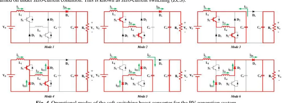
Shown in Fig. 4, the operational principle of this converter can be divided into six intervals. For a simple analysis of each interval of this converter, the following assumptions are made.All switching devices and passive elements are ideal.
1) The parasitic components of all switching devices and elements are negligible. 2) The input voltage ( V s) is in the range of 150–230 V.
3) This converter operates the continuous conduction mode at all intervals.
A . I n t e r v al 1 (t ₒ ₒ t < t1)
Switches S1 and S2 are both in the OFF state, the current cannot flow through switches S1 and S2, and the accumulated energy of the main inductor is transferred to the load (Fig. 5). In this interval, the main inductor current decreases linearly. During this time, the current does not flow to the resonant inductor, and the resonant capacitor has charged as output voltage
After two of the switches have been turned on, interval 1 is over. These conditions are as follows:
B . I n t e r v a l 2 (t 1 ₒ t < t 2)
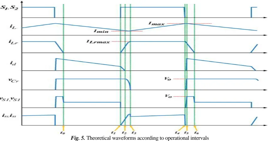
After turning on switches S1 and S2, the current flows to the resonant inductor. At that time, two of the switches are turned on under zero-current condition. This is known as zero-current switching (ZCS).
Fig. 5. Theoretical waveforms according to operational intervals
Because the main and auxiliary switches implement ZCS, this converter has lower switch loss than the conventional hard-switching converter. As the resonant current rises linearly, the load current gradually decreases. At t2, the main inductor current equals the resonant inductor current, and the output diode current is zero. When the resonant capacitor voltage equals
V o, the output diode is turned off, and interval 2 is over
C . I n t e r v a l 3 (t 2 ₒ t < t 3)
The current that flowed to the load through output diode D o no longer flows, since t2 and the resonant capacitor C r,
and the resonant inductor L r start a resonance. The current flowing to the resonant inductor is a combination of the main inductor current and the resonant capacitor current. The amount of resonant current is expressed as (14)
During this resonant period, the resonant capacitor C r is discharged from V o to zero. This is expressed as (15). Resonant frequency and impedance are given by (16) and (17). When the voltage of the resonant capacitor equals zero, the interval 3 is over
D. Interval4 (t 3 ₒ t < t 4)
After the resonant period in interval 3, when the voltage of the resonant capacitor equals zero, interval 4 begins.
In this interval, the freewheeling diodes of D1 and D2 are turned on, and the current of the resonant inductor is the max-imum value. The resonant inductor current flows to the free-wheeling diodes S1-Lr-D2and S2-Lr-D1along the freewheeling path
E. Interval5(t 4 ₒ t < t 5)
In interval 5, all of switches are turned off under the zero-voltage condition by the resonant capacitor. During this interval, the initial conditions of the resonant inductor current and resonant capacitor voltage are as follows:
When all of the switches are turned off, the resonant capacitor C r is charged to the output voltage by two of the inductor currents. Until the resonant capacitor has been charged to V o , the output diode is in the OFF state
F. Interval6(t 5ₒt < t 6)
Interval 6 begins when the resonant capacitor equals the output voltage, and the output diode is turned on under the zero-voltage condition. During this interval, the main inductor current i L and the resonant inductor current i L r flow to the output through the output diode D o
At that time, two of the inductor currents are linearly de creased, and the energy of the resonant inductor is completely transferred to the load. Then, the interval 6 is over
Fig. 6. ZVS condition
IV.
DESIGN PROCEDURE OF RESONANT INDUCTOR AND CAPACITOR IN SARC
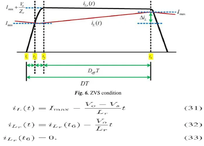
A. ZVS Condition of Switch
During interval 4, the voltage of the resonant inductor and the current are expressed by (36) and (37), respectively. The ZVS condition of this converter is expressed by (38)
B. Resonant Inductor
In Fig. 6, the time of interval 2, which is the rising time of the resonant inductor current, is expressed by (41). For the maximum resonant current, the time of interval 3, which is the resonant time of the resonant inductor and capacitor, is defined as one-fourth of the resonant period. As a rule of thumb, the rising time of the resonant inductor current (intervals 2– 3) can be set to 10% of the minimum on time. This is expressed as (43)
From (40) and (43), the resonant inductor expressed as
C . R e s o n a n t C a p a c i t o r
The resonant capacitor is connected to the switch in parallel. Thus, the waveforms of the resonant capacitor voltage and switch voltage are equivalent at turn -off. To satisfy the ZVS condition, the resonant capacitor can be selected to exceed ten times the output capacitance o f the switch. However, the capacitor is charged by the main inductor current and the resonant inductor current at turn -off. Thus, it can be selected to exceed twenty times the output capacitance of the switch. Equation (43) is simplified to
The design of the resonant inductor and capacitor are based on (44) and (45).
V.
SIMULATION RESULTS
This paper simulated the adopted soft-switching boost converter and the PV module modeling of 700 W using the PSIM software. Fig. 7 shows the simulated output characteristic waveform of the PV module, which controlled the MPPT using dynamic link libraries (DLLs) for the PSIM software. At 0.4 s, this converter starts estimating the maximum power point. After 0.925 s, the MPPT is completed. At this time, the simulated PV module reaches the maximum power of 700 W, and then, the output voltage and current of simulated PV module are 194.3 V and 3.6 A, respectively.
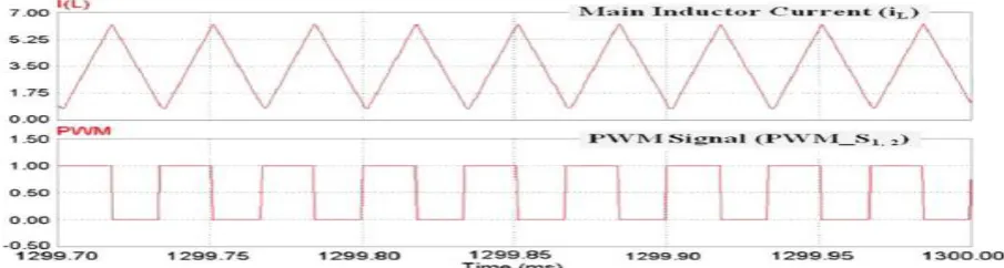
Fig. 8 shows the main inductor current and the pulsewidth modulation (PWM) gate signal of the main switch. When the main switch is turned on, the energy of inductor is accumulated. When it is turned off, this energy is transferred to the output.
Fig. 9 shows the waveforms of the output diode voltage and the current.
Fig. 10 shows the waveforms of the resonant capacitor volt-age and the resonant inductor current.
Fig. 7. Simulated output characteristic waveforms of PV module. (a) Simulated I–V and power curves of PV module. (b) Simulated real-time waveforms of power, voltage, and current.
Fig. 8. Simulated waveforms of the gate signal and the main inductor current.
Fig. 10. Simulated waveforms of the resonant capacitor voltage and the resonant inductor current.
Fig. 11. Simulated waveforms of the main switch voltage and the current.
Fig. 12. Experimental setup using the Solarsim-10k PV simulator.
VI.
EXPERIMENTAL RESULTS
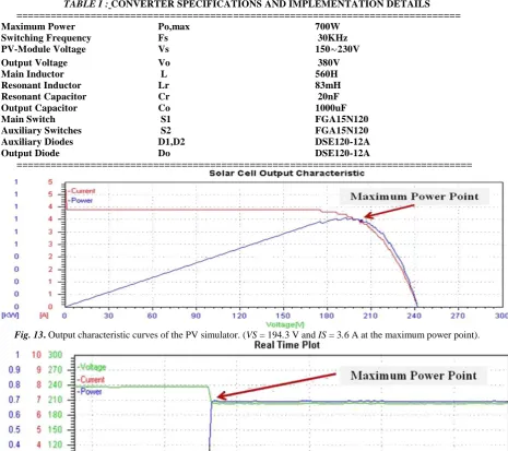
Switching Frequency Fs 30KHz
PV-Module Voltage Vs 150 230V
Output Voltage Vo 380V
Main Inductor L 560H
Resonant Inductor Lr 83mH
Resonant Capacitor Cr 20nF
Output Capacitor Co 1000uF
Main Switch S1 FGA15N120
Auxiliary Switches S2 FGA15N120
Auxiliary Diodes D1,D2 DSE120-12A
Output Diode Do DSE120-12A
================================================================================
Fig. 13. Output characteristic curves of the PV simulator. (VS = 194.3 V and IS = 3.6 A at the maximum power point).
Fig. 14. Real-time voltage, current, and power waveforms of PV simulator. (PS = 700 W, VS = 194.3 V, and IS = 3.6 A at
the maximum power point).
In this paper, the irradiance and operating temperature of the Solarsim-10k PV simulator were set as 0.9 kW/m2 and 25 ◦C, respectively. Fig. 13 shows the V –I and V –P characteristic curve of the PV simulator used as the source of this converter. Oscillations at the edge of the characteristic curve are controlled by the maximum power point. Based on this waveform, the converter controlled the MPPT effectively. Fig. 14 shows the current, voltage, and power with respect to time for the maximum power point. Based on this graph, the output voltage and current were 194.3 V and 3.6 A, respectively, and the output power reached 700 W at the maximum power point.
Fig. 15 shows the waveform of the main inductor current and the gate signal. By the PWM signal, the rising current
Fig. 15. Measured waveforms of the main inductor and the gate signal (y-axis: iL = 4 A/div and PWMS1,2 = 10 V/div; x -axis: 10 μs/div).
Fig. 16. Measured waveforms of the output diode voltage and current (y-axis: VDo = 200 V/div and iDo = 4 A/div; x-axis:
10 μs/div).
Fig. 16 shows the current and the voltage waveform of the output diode. Based on this waveform, the diode is turned on under zero-current condition, and it is turned off under zero voltage condition. Thus, the switching losses of the diode can be reduced.
Fig. 17 shows the resonant inductor current, the resonant capacitor voltage, and the load voltage. When charging and discharging the capacitor, it is in resonance with the resonant inductor.
Fig. 18 shows the switch current and voltage waveforms, when the switch is turned on under zero-current condition by the resonant inductor and it is turned off under zero-voltage condition by the resonant capacitor.
Fig. 19 shows the efficiency of the proposed converter. As shown, the efficiency of the proposed converter is improved by about 4%.
Fig. 17. Measured waveforms of the resonant inductor current and resonant capacitor voltage (y-axis: VCr = 200 V/div and
Fig. 18. Measured waveforms of the main switch voltage and current (y-axis: VS1 = 200 V/div and iS1 = 4 A/div; x-axis: 10
μs/div).
Fig. 19. Efficiency under the entire load conditions.
In this paper, the efficiency is measured as follows. The power supply (KJP-18K) is connected to the input of the converter, and the electric load (EL-3000P) is connected to the output. Moreover, the converter is tested by varying the load. The efficiency is measured by the power analyzer PM 3000A. We compared the conventional hard-switching converter and the adopted converter under the same switching frequency and power conditions.
VII.
CONCLUSION
In this paper, we proposed a soft-switching boost converter, which involved an added SARC in the conventional boost converter. This soft-switching boost converter is easy to control because the two switches are controlled by the same PWM signal. All of the switching devices in this converter achieved ZCS and ZVS by the resonant inductor and capacitor at turn/off. Therefore, the switching losses were reduced dramatically. This paper has analyzed the operational principles of the adopted converter and applied them to the P&O algorithm, which is a kind of MPPT method. Moreover, this converter was verified by the simulation and experimental results. This soft-switching boost converter can be applied to a stand-alone and a grid-connected system using a PV power conditioning system
REFERENCES
[1]. R. Gules, J. De Pellegrin Pacheco, H. L. Hey, and J. Rnhoff, “A maximum power point tracking system with parallel connection for PV stand alone applications,” IEEE Trans. Ind. Electron., vol. 55, no. 7, pp. 2674–2683, Jul. 2008.
[2]. F. Liu, S. Duan, F. Liu, and Y. Kang, “A variable step size INC MPPT method for PV system,” IEEE Trans. Ind. Electron., vol. 55, no. 7, pp. 2622–2628, Jul. 2008.
[3]. H. Bodur and A. Faruk Bakan, “A new ZCT-ZVT-PWM DC–DC converter,” IEEE Trans. Power Electron., vol. 19, no. 3, pp. 676–684, May 2004.
[4]. J.-H. Kim, D.-Y. Yung, S.-H. Park, C.-Y.Won, Y.-C. Jung, and S.-W. Lee, “High efficiency soft-switching boost converter using a single switch,” J. Power Electron., vol. 9, no. 6, pp. 929–939, Nov. 2009.
[5]. J.-P. Lee, B.-D. Min, T.-J. Kim, D.-W. Yoo, and J.-Y. Yoo, “Design and control of novel topology for photovoltaic dc/dc converter with high efficiency under wide load ranges,” J. Power Electron., vol. 9, no. 2, pp. 300–307, Mar. 2009.
[6]. J.-J. Lee, J.-M. Kwon, E.-H. Kim, and B.-H. Kwon, “Dual series resonant active clamp converter,” IEEE Trans. Ind. Electron., vol. 55, no. 2, pp. 699–710, Feb. 2008.
[7]. X. Wu, J. Zhang, X. Ye, and Z. Qian, “Analysis and derivations for a family ZVS converter based on a new active clamp ZVS cell,” IEEE Trans. Ind. Electron., vol. 55, no. 2, pp. 773–781, Feb. 2008.
[9]. M. Z. Youssef and P. K. Jain, “Series parallel resonant converter in self sustained oscillation mode with the high frequency transformer leakage inductance effect: Analysis, modeling, and design,” IEEE Trans. Ind. Electron., vol. 54, no. 3, pp. 1329–1341, Jun. 2007.
[10]. R. Casanueva, F. J. Azcondo, and C. Branas, “Output current sensitivity analysis of the LCpCs resonant inverter: Current source design criteria,” IEEE Trans. Ind. Electron., vol. 54, no. 3, pp. 1560–1568, Jun. 2007.
[11]. S. Zheng and D. Czarkowski, “Modeling and digital control of a phase controlled series parallel resonant converter,” IEEE Trans. Ind. Electron., vol. 54, no. 2, pp. 707–715, Apr. 2007.
[12]. D. J. Tschirhart and P. K. Jain, “A CLL resonant asymmetrical pulse width modulated converter with improved efficiency,” IEEE Trans. Ind. Electron., vol. 55, no. 1, pp. 114–122, Jan. 2008.
[13]. N. D. Benavides and P. L. Chapman, “Modeling the effect of voltage ripple on the power output of photovoltaic modules,” IEEE Trans. Ind. Electron., vol. 55, no. 7, pp. 2638–2643, Jul. 2008.
[14]. G.-R. Cha, S.-H. Park, C.-Y. Won, Y.-C. Jung, and S.-H. Song, “High efficiency soft switching boost converter for photovoltaic system,” in Proc. 13th EPE-PEMC, Sep. 1–3, 2008, pp. 383–397.