Implementation of FFT Processor on FPGA
Shruti Ashok Joshi
1, Nitesh Guinde
21
Department of Electronics and Telecommunication, Goa College of Engineering, Farmagudi-Goa
2
Associate Professor, Department of Electronics and Telecommunication, Goa College of Engineering, Farmagudi-Goa
Abstract- Various processing applications such as video processing, audio processing, RF signal processing, image processing etc. include computation of transforms such as FFT. Computation of FFT sample is expensive in terms of speed, performance and throughput. The software N-point FFTs are reprogrammable but slow, which is a disadvantage. Two solutions are possible to alleviate the above problem. One is to move the design to an ASIC, a complete hardware solution. Although, it improves the system performance, the ASIC is not reprogrammable, or reconfigurable. The second is, design of FFT processor using hardware-software co-design on FPGA, which is reconfigurable and has high throughput. This paper describes a hardware-software co-design of a FFT using a ZynqSoC. This SoC tightly couples the programmable logic with a dual core Cortex ARM processor. It provides low latency, high throughput and cache coherent communication between programmable logic and the ARM processor. Zedboard is one such platform, and is used in the implementation of the project. This design could be inserted into any embedded application which has a FFT computation involved in it. Keywords: Zynq-7000 SoC, Zedboard, IP core, Linux kernel device driver
I. INTRODUCTION
Discrete Fourier Transform (DFT) transforms a signal (or discrete sequence) from the time domain representation to the frequency domain.DFT is used to calculate the frequency spectrum of a signal, for which it uses the information encoded in frequency, phase and amplitude of the component sinusoids.DFT can also be used to find the frequency response of a system from its impulse response. The direct evaluation of DFT for N samples requires N2 complex multiplications and N (N-1) complex additions. Thus, for large values of N, inordinate amount of calculation will be required. By using FFT algorithms, the number of calculations can be reduced. Fast Fourier Transform (FFT) is an efficient algorithm for calculating the DFT.For N point DFT,only N/2 log2 N number of complex multiplications
are required using FFT.
Signal Processing modifies acquired time-series data for the purpose of analysis or enhancement. Examples of signal processing include spectral analysis and enhancing acquired data using digital filtering. The algorithmsused for signal processing use FFT to characterize the magnitude and phase of a signal. It is also used in combination with other operations to perform more involved computations such as convolution or correlation.FFT computation is also widely used in image or video processing applications. In image processing applications, FFT is used to convert an image from image (spatial) domain to frequency domain. Applying filters to images in frequency domain is computationally faster than to do the same in the image domain.
FFT algorithm needs to perform N/2 log2 N complex multiplications and N log2 N complex additions for N input
samples. If N>1024, then the number of computations required, also increase. This makes FFT computation, a challenge.FFT algorithms can be implemented as a software code. But it is generally constrained to execute instructions serially (one at a time) and is therefore severely constrained by the processor instruction throughput. Thus, computation of FFT samples becomes slower. As an alternative to software FFT, hardware FFT can be implemented. The hardware FFT performs many of its processing tasks in parallel, hence can achieve order-of-magnitude throughput improvements over software FFTs executed in DSP microprocessors. But, the size and speed of the logic designed must be kept at a practical scale.Also, as the number of computations increase, the power consumption of the FFT increases. Since hardware FFT is a separate unit, a software-controlled coprocessor is required for communication with the processor. Hardware software co-design of FFT on SoC, gives the advantages obtained from software as well as hardware FFT. Such design is reconfigurable and has high throughput. Power consumption of FFT implemented on SoC is also low.
GNU Radio enables users to design, simulate and deploy real world radio systems, such as audio processing, mobile communications, tracking satellites, radar systems, GSM networks, Digital Radio Mondiale etc. Almost all the radio system applications mentioned, use FFT module for spectral analysis. This software development kit provides a comprehensive library of processing blocks that can be combined to make complex signal processing applications.
II. RELATED WORK
The construction of the Cooley-Tukey Decimation-In-Time algorithm for implementation in an FPGA is described in [2]. In this paper, the basic DFT algorithm is explained. The DIT (decimation in time) and DIF (decimation in frequency) forms of FFT are also discussed further, and DIT FFT algorithm is preferred. For implementation of full transform, an address generator, a butterfly operator, a memory and twiddle factor generator are required. The construction of software transform is also explained in this paper further. The software transform is constructed by first doing the permutation of the input data and then carrying out the butterfly operations. A comparison of performing FFT in hardware and in software is carried out in [2] and s 32 point FFT in hardware using 11 bit signed integer input data is implemented.
In [11], an adaptive FFT program that tunes the computation automatically for any particular hardware is proposed. On general-purpose microprocessors, the performance of a program is mostly determined by complicated interactions of the code with the processor pipeline, and by the structure of the memory. In this paper, this problem is addressed by using an adaptive approach, where the program itself adapts the computation to the details of the hardware. A FFTW, an adaptive, high performance implementation of the Cooley-Tukey fast Fourier transform (FFT) algorithm written in C is developed in this paper. The runtime structure for FFTW is discussed in this paper. The FFTW is compared with over 40 implementations of FFT on 7 machines. From this comparison, [11] infers that the self optimizing approach of FFTW yields better performance than all other publicly available approaches. [7] Provides an overview of the FIR filter FPGA accelerator example in GNU Radio with the ZynqSoC, and a tutorial on how to setup the necessary hardware and software. This document provides the pre-built files such as rootfs, SDK and boot files, required for building GNU Radio. Further, in this document, the procedure of building Linux kernel, u-boot, and root file system with open embedded is also explained. A high level overview of the components of FPGA accelerated FIR filter example, is discussed in detail. The procedure of preparing a bootable card and configuring the hardware to boot from the SD card is also explained. This paper further explains the procedure to install GNU Radio FPGA accelerated FIR filter module. Finally, a comparison of the performance of the pre-existing software FIR filter and FPGA accelerated FIR filter is carried out.
Based on the information provided in the document [7], FPGA accelerated FIR filter example was tried on Zedboard. Bitstream for the HDL design was generated successfully using the pre-built files. Also FSBL (First Stage Boot loader), binary file of the design and a bootable SD card were also implemented. But installation of GNU Radio FPGA accelerated FIR filter module could not be completed.
A study that focuses on the FPGA implementation of a reconfigurable FFT operator is discussed in [1].According to the author of [1], the designed FFT operator can provide Fourier transforms over complex infinite field X and Galois finite field GF. Also, it exploits the possibility to share hardware resources when considering multi-standard scenarios for software radio systems. The technology proposed in this paper is connected to consumer handheld devices in which FFT is involved.
Zedboard is a development board for Zynq-7000 all programmable SoC as mentioned in [14].The specifications of this platform are discussed in [14].The Zynq-7000 SoC tightly couples a dual core Cortex A9 ARM processor with the programmable logic[9].The other features of this SoC are also mentioned in [9].
Based on the study of FFT algorithm, Zedboard and the example in [7], the chosen aim of the project was, implementation of FPGA accelerated FFT.All the important components of this project are discussed in the following sections.
III. CONCEPTUAL DESIGN
Figure (a): Conceptual design
IV. RECONFIGURABLE HDL LOGIC BLOCK
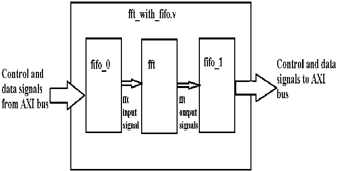
As mentioned earlier, this paper presents a methodology to implement a computationally expensive unit in hardware. Also for improving the performance of a signal processing application, FFT (Fast Fourier Transform) unit must be implemented in hardware. The FFT unit is considered computationally expensive, because computation of FFT samples is time consuming. It reduces the efficiency if entire application. To implement FFT unit as a reconfigurable block, certain aspects need to be considered. According to the conceptual design, shown in figure (a), the reconfigurable logic block must communicate with the AXI peripheral bus. But, for this communication, the operating speed of both, the FFT and the AXI peripheral bus should be synchronized. Otherwise, some of the input or output FFT samples could be lost. Thus, the design shown in figure (b) must be implemented. As shown in this figure, the FFT unit is connected to 2 FIFO units, one at the input and the other at the output of the FFT unit. These FIFO units retain the input or output samples. The control and data signals from AXI peripheral bus is stored in fifo_0.It generate output signals, which are FFT input control and data signals. The FFT output signals are saved in fifo_1, which supplies its output signals as control and data signals to AXI peripheral bus. The design in figure (b) is implemented in Verilog, as a reconfigurable logic block.
V. AXI PERIPHERAL BUS
Xilinx’s AXI peripheral bus is a part of ARM AMBA bus. There are 3 types of AXI4 interfaces as mentioned below. (i) AXI4 Full: It provides high performance and has memory mapped requirements.
(ii) AXI4 Lite: It allows simple, low throughput memory mapped communication. (iii) AXI4 Stream: It allows high speed streaming data.
The proposed design uses AXI4-Lite peripheral bus. This bus consists of lesser connections than that for full and full or stream buses. Also, Lite bus supports the data transfer required in this design. It has got a simplified link, and supports memory mapped data transfer. Thus, single address and word data transfer is possible. It consists of 32 bit data bus width, 64 bytes memory, and 4 registers. It also consists of 5 channels, namely, read and write address channels, read and write data channels, and a write response channel. But, this bus allows burst transaction of up to 256 data transfers only.
VI. BOOTABLE SD CARD
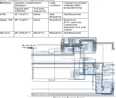
The PL is a HDL design. It needs to be ported to FPGA, which is Zedboard, in this case. A system design that is compatible with Zedboard and FMCOMMS2 combination, is shown in figure (c).This design consists of ADCs, DACs, AXI interconnect, Zynq PS, etc; and can be generated easily. The design that consists of 2 FIFOs and a FFT unit, connected to AXI peripheral bus, constitutes the fft_with_fifo IP core. This core is integrated with the design shown in figure (c). For implementing a computationally expensive unit in hardware, the design shown in figure (c), along with the fft_with_fifo IP core, must be synthesized, implemented and the bitstream should be generated. Programming the Zedboard with a bitstream, can be done in 3 different ways, which compared in table I. The JTAG method of programming is the simplest among all. In this, bitstream is directly ported to the FPGA through JTAG port. In Quad SPI method, the bitstream is ported to flash memory. In SD card programming method, FSBL (First Stage Boot loader), uboot.elf (Second stage boot loader), and HDF (Hardware Description File) are required. In the previous two methods, these two files are not needed. To implement the proposed design, the SD card programming method is suitable. For this, the above mentioned files must be generated and further used, to create a binary file,’BOOT.BIN’.This binary file is loaded on a SD card, compatible with the Zedboard and consists of Linux image of suitable version.
Table 1 Comparison Of Programming Methods
VII. LINUX DEVICE DRIVER
The Linux device driver is a C code, which performs functions such as opening a specific file, mapping the virtual and the physical addresses, data transfer between the processor and the designed IP core. The driver code used for the proposed design consists of following important functions.
(i) open ("/dev/mem", O_RDWR | O_SYNC);
(ii) mmap (0, MAP_SIZE, PROT_READ|PROT_WRITE, MAP_SHARED, memfd, dev_base& ~MAP_MASK); (iii) munmap (mapped_base, 4096);
The driver allocates fixed pages of memory for the processor, or the PL data transfer. Thus, user program can transfer data, into and out of the FPGA fabric. The driver exposes AXI Lite slave memory mapped address space and also handles interrupts.
VIII. CONCLUSION
A methodology for implementing a computationally expensive unit as an IP core that is driven using a Linux driver has been described in this paper. Although the work implemented is confined to Zedboard and FMCOMMS2 combination, implementation for other combinations of Zynq platform is also possible.
The design proposed in this paper, is limited to the implementation of FPGA accelerated FFT, further implementations can make this FPGA accelerated FFT module to improve the performance of software applications, running on ARM processor.GNU Radio and IIO Oscilloscope are two applications that run on ARM processor.GNU Radio software is used to design real-time radio systems.IIO Oscilloscope is a spectrum analyzer, and can be used to view and study signals. In both these applications, use of FFT module can be required. Due to the reasons mentioned earlier, use of FPGA accelerated FFT module, would improve the speed and efficiency of these applications.
IX. REFERENCES
[1] Ali Al Ghouwayel and Yves Louët,”FPGA Implementation of a Re-configurable FFT forMulti-standard Systems in Software Radio Context”,May 2009,IEEE Transactions on Consumer Electronics, Vol. 55
[2] G. William Slade,” The Fast Fourier Transform in Hardware: A Tutorial Based on an FPGA Implementation”, March 21, 2013 [3] http://man7.org/linux/man-pages//man2/munmap.2.html
[4] https://wiki.analog.com/resources/eval/user-guides/ad-fmcomms2-ebz/software/linux/zynq_2014r2 [5] https://wiki.analog.com/resources/fpga/docs/build
[6] http://www.fpgadeveloper.com/2014/08/creating-a-custom-ip-block-in-vivado.html [7] https://wiki.gnuradio.org/index.php/Zynq
[8] https://www.xilinx.com/support/documentation/ip_documentation/axi_ref_guide/v13_4/ug761_axi_reference_guide.pdf [9] https://www.xilinx.com/support/documentation/data_sheets/ds190-Zynq-7000-Overview.pdf
[10] https://www.xilinx.com/support/documentation/sw_manuals/xilinx2014_1/ug910-vivado-getting-started.pdf
[11] Matteo Frigo, Steven G. Johnson,” FFTW: AN ADAPTIVE SOFTWARE ARCHITECTURE FOR THE FFT”, 1998 IEEE International Conference on Acoustics, Speech and Signal Processing, ICASSP '98
[12] Muhammed Al Kadi, Diana Gohringer,Michael Hubner,Patrick Rudolph, “Dynamic and partial reconfiguration of Zynq 7000 under Linux”, 2013 International Conference on Reconfigurable Computing and FPGAs (ReConFig)
[13] Yan Han,Erdal Orukulu,”Real time traffic sign recognition based on Zynq FPGA and ARM SoCs” , IEEE International Conference On Electro/Information Technology