©2012 JNAS Journal-2013-2-1/19-24 ISSN 0000-0000 ©2012 JNAS
A Low Power, Glitch Free Programmable Divider in 0.18µm CMOS
Technology
Ebrahim Abiri
*, Mohammad Reza Salehi and Sanaz Salem
Electrical and Electronic Department of Shiraz University of Technology
Corresponding author Email :
[email protected]
ABSTRACT: A low power programmable frequency divider is proposed in this paper which is appropriate for WLAN applications. Multi- modulus architecture in dynamic logic with the minimum number of transistors is designed in 0.18µm CMOS technology. By using mixer, bandpass filter and switches, the divide ratios improved to 18. A technique is implemented in the dynamic 2-3 programmable divider cell for decreasing the glitches which leads to low power consumption. Based on simulation results it works up to 5GHz, with the average power about 37nW. Under a supply voltage of 1.8V, the total chip area of the multi- modulus programmable divider is 3100µm2.
Keywords: 2-3 Programmable divider cell, Divide ratio, Glitchless, Multi- modulus, Low power
consumption.
INTRODUCTION
Programmable frequency divider is one of the main and basic building blocks which has an important role in frequency synthesizer for the purpose of stability, spectrum purity and frequency range in the developing of computers, global systems, mobile communication, digital TV, GPS, radar and telecontrol measures (Zhiqiang et al., 2010; Kim et al., 2011). In addition, frequency divider is an integral part of the PLL taking the input frequency from the VCO and generating one or more high quality frequencies which is appropriate for analog front- end circuits (Zhiqiang et al., 2010; Sleiman et al., 2008). Therefore the design of frequency divider is critical and tricky in order to reach the advantages of high speed, high sensitivity, low power consumption and better programmability (Sleiman et al., 2008; Lin et al., 2009; Francesco et al., 2008).
In general frequency divider categorize into two groups, analog and digital (Ching et al,. 2009). Regenerative frequency divider and the injection locking frequency divider (ILFD) belong to the analog frequency dividers while the static and dynamic logic dividers are included in digital frequency dividers. Since the dynamic logic has benefits of high speed and programmability, it is more common in the application of communication systems (Ting et al,. 2010).
20
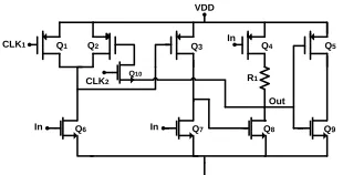
which leads to more power consumption and an increase in the complexity of the designs (Tarek and Kaamran, 2010). For overcoming the disadvantages of the conventional topologies, the single stage divide- by- 2/3 is presented. The TSPC divide- by- 2/3 cell which consists of only 10 transistors is shown in Fig.1. This architecture is designed for the VCO input source in the range of WLAN frequencies. The control signals which activate transistors Q1 and Q2 can change the division ratio from 2 to 3, respectively.
Q1 Q2
CLK1
CLK2
Q3
In Q4
VDD
Out
Q8
Q7
In In Q6
Q5
Q9
Q10
Figure 1. The TSPC divide- by- 2/3 cell
Figure 2 shows the simulation results of the two division ratios. As it is clear the glitches make the problem in the high quality operation of frequency divider in high speed.
Figure 2. The divide- by- 2 and divide- by- 3 results related to Vin
To avoid glitches, the proposed glitch free architecture is shown in Fig. 3. The high value of resistor R1 can
decrease the voltage level and as a consequence the glitches can disappear easily in this design. Given the fact that the resistor consumes more power and increases the chip area, so the best value for it should be selected to establish a trade-off between the power consumption, chip area and the level voltage of glitches. The simulation results for the divide- by- 2/3 with the glitches resistor technique are shown in Fig. 4. Comparing with the last results it can be widely cleared that the glitches diminish in the new structure.
Q1 Q2
CLK1
CLK2
Q3
In
Q4
VDD
Q5
Q9
Out
R1
Q8
Q7
In
In Q6
Q10
21
Figure 4. The divide- by- 2 and divide- by- 3 results with glitch free technique
Multi- mode programmable frequency divider
There are various architectures providing the wide range of division, such as pulse swallow dividers, cascaded dual- modulus dividers and phase rotating dividers (Hesham et al., 2011). The major drawbacks of these structures are the high power consumption and the need for extra extension logic and input buffer circuits in order to ensure correct operating of dividers with large signal swing (Sleiman et al., 2008; Nesreen and Masuri, 2009; Qinqing and Zhiqun, 2012). In this paper a multi- mode programmable frequency divider with the switching technique, one or two divide- by- 2/3 cells, a radio frequency (RF) mixer and a band- pass filter (BPF) are proposed. All the switches play an essential role in preparing the different division ratios by setting into “ON” and “OFF” states. Considering the fact that the number of divide- by- 2/3 cells is limited, not only does the power consumption remain low, but also the complexity of the extra structures like input buffer and extension logic circuit can be ignored easily. The proposed block diagram of the multi- mode programmable frequency divider is shown in Fig. 5. The mixer in this structure has two inputs to produce the output frequencies of the summation and subtraction of the two inputs. It is clear that the band- pass filter should remove the higher frequency of the summation of two inputs; therefore the output of the band- pass filter is the subtraction of two signals for the purpose of fine operating of the circuit.
For the purpose of fine operation, capacitor is used for coupling the stages. In this situation the effect of each stage on the whole circuit is diminished significantly. Although capacitors increase the chip area, play a key role in decreasing the power consumption and fining the output signal. Thus the value of the capacitor is determined based on the trade- off between the power consumption and chip area.
SW1
BPF SW0
div1
SW3 div2
SW4 SW2 Vin
Vout
Figure 5. The proposed block diagram of the multi- mode programmable divider
The circuit of mixer and band- pass filter is proposed in Fig. 6. As it is shown in this figure the active inductor is used in this architecture to decrease the chip area while it operates in a double- balanced configuration. The mixer receives two frequencies from input stage and LO stage, then the band- pass filter passes only the subtraction of two frequencies and ignores the higher frequency from the summation of fin and fLO . It is important to note that the
input frequency should be appropriately selected based on the operation frequency of both dividers, mixer and band- pass filter. As it is mentioned, the dividers are designed to work under WLAN frequencies, while the mixer and band- pass filter can work up to WLAN frequencies. Another crucial factor is the accurate selection of clock signals for switches in order to have the exact output of stages and consequently to reach the desired range of frequency divider from 2 to 18. Therefore the suitable combination of all blocks and switches culminates in the glitch free output signal of the programmable frequency divider.
M1 M2
M3
M4 M5
M6 M7
M8 M9
M10 M11
M12 M13
M14M15
M16 M17 out2
out1
In In
SW3
SW2 SW4
VDD
Vctrl1
Vctrl2
22
in out
out out in
V V 1
V V V
2 3
(2)
in out
out out in
V V 1
V V V
3 4
(3)
in
out out out in
1 V
V V V V
3 6
(4)
For the rest of modes two divide- by- 2/3s should be worked to achieve the best operation of the programmable divider. In this case the power consumption reaches to its maximum about 37nW The equations based on modes 1/8, 1/12 and 1/18 can be calculated as follows:
in out
out out in V
2V 1
2 V V V
2 8
(5)
in out
out out in V
3V 1
2 V V V
3 12
(6)
in out
out out in
V 3V
1
3 V V V
3 18
(7)
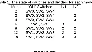
Table 1 summarizes the different states of switches and dividers for the various modes of the frequency divider. It is absolutely certain that with the help of simple switches, the several ranges of frequencies can be produced without any need of sophisticated topologies in previous literatures.
Table 1. The state of switches and dividers for each mode
Mode “ON” Switches div1 div2
2 SW0, SW2, SW4
3 SW0, SW3, SW4 2
4 SW0, SW3, SW4 3
6 SW1, SW2 3
8 SW1, SW2, SW3 2 2
12 SW1, SW2, SW3 2 3
18 SW1, SW2, SW3 3 3
RESULTS
A simulation of the WLAN frequency divider has been realized in 0.18µm CMOS technology. The implemented division ratios are improved in to 2-18 frequency modes under 1.8V power supply. The figure of merit of the multi- modulus programmable frequency divider based on the definitions of maximum input frequency (fmax) in GHz, voltage supply (VDD) in volt and the average power consumption (P) in mW can be expressed as follows:
3 max
f
η ( P.VDD )75 10 (8)
23
Figure 8. Input, control signals and output voltages
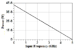
Thanks to the one stage of the proposed structure instead of using four D- latches in the conventional divide- by- 2/3, the power consumption measures as low as 4nW and for the high division ratios with switching technique topology reaches to 37nW. Figure 9 shows the power consumption proportional to the operating frequencies for the multi- modulus divider; as a result of low number of transistors it is much lower than the conventional architectures.
Figure 9. Power consumption versus input frequency
The layout of the proposed programmable divider is shown in Fig. 10. Comparing with the conventional divider with four D- latches, it consumes 3080µm2 which is much less than the previous structures. Table 2 demonstrates the comparison between the proposed design and some conventional circuits published recently. It goes without saying that the presented multi- stage programmable divider has the lowest power consumption with the minimum chip area in the same technology as the other literatures.
Figure 10. The layout of the proposed divider
Table 2. Characteristics comparison
Dividing ratio Supply voltage (v) Power consumption Fmax (GHz) Chip area Technology (µm CMOS)
[1] 120- 400 1.8 - 2.2 - 0.18
[2] 13- 1278 1.5 3.23 mW 3.5 0.0408 mm2 0.18
[3] 8- 255 1.8 11 mW 7.55 6630 µm2 0.18
[7] 2- 3 1.8 3.24 mW 5.8 2000 µm2 0.18
[9] 2403- 2480 1.8 7.7 mW 6.5 0.02 mm2 0.18
[10] 8- 9 1 0.29 mW 6 400 µm2 0.18
[13] 15- 16 1.8 0.7 mW 3.4 - 0.18
[14] 720- 960 1.8 3.24 mW 3 5400 µm2 0.18
This work 2- 18 1.8 37nW 5 3100 µm2 0.18
CONCULSION
24
2009.
Joonhee L. 2011. Sunghyun Park, SeongHwan Cho, 19(1): 61- 70.
Hesham O, Khaled S, Magdi I. 2011 A low-power digital frequency divider for system-on-a-chip applications. Paper presented at the IEEE 54th international midwest symposium circuits and systems (MWSCAS), 2011.
Francesco B, Padmanava S, Saikat S, Stephane P, Joy L. 2008 Programmable frequency-divider for millimeter-wave PLL frequency synthesizers. Paper presented at the IEEE 38th european microwave conference, 2008.
Kim K, Min Y, Kim S, Park J. 2011. IEEE IET circuits devices system 5: 170- 176.
Lin Y, Lu C, Wang Y. 2009 A 24-GHz triple-mode programmable frequency divider in 0.13-µm CMOS technology. Paper presented at the IEEE microwave conference APMC, Asia Pacific, 2009.
Nesreen I, Masuri O. 2009 CMOS programmable divider for Zigbee frequency synthesizer. Paper presented at the IEEE international conference on signals, circuits and systems, 2009.
Qinqing C, Zhiqun L. 2012 Design of a low power 2GHz CMOS frequency divider for WSN applications. Paper presented at the IEEE international conference microwave and millimeter wave technology (ICMMT), 2012.
Sleiman B, Jad G, Saul R, Ana R, Mohammed I. 2008 Wide-division-range high-speed fully programmable frequency divider. Paper presented at the joint 6th international IEEE northeast workshop on circuits and systems and TAISA conference, 2008.
Sun Z, Li Z. 2011 Design of a low-power high-speed CMOS frequency divider for WSN applications. Paper presented at the IEEE 13th international conference on communication technology (ICCT), 2011
Tarek K, Kaamran R. 2010 An ultra-low power 200 MHz-1 GHz programmable frequency divider with novel clear/preset d-latch. Paper presented at the IEEE International Midwest Symposium Circuits and Systems (MWSCAS), 2010.
Ting-Hsu C, Chi-Sheng L, Chin-Long W, Ying-Zong J, Chun-Ming H. 2010 High-speed and low-power programmable frequency divider. Paper presented at the IEEE International Symposium on Circuits and Systems (ISCAS), 2010.
Xiaopeng Y, Jianjun Z, Xiaolang Y, Wei L, Manh A,Kiat S. 2008 Sub-mW multi-GHz CMOS dual-modulus prescalers based on
programmable injection-locked frequency dividers. Paper presented at the IEEE radio frequency integrated circuits symposium, 2008.