Visakhapatnam, Andhra Pradesh, India
Abstract: in today’s advance electronic and communication systems the role of high accuracy analog to digital converters are of great importance. Nowadays, a larger percentage of mixed-signal applications requires for health care systems. Also the speed of the chosen ADC design matters a lot as we are connected with the real world signals. SAR based ADC will provides us a better solution for various analog to digital systems. It is an essential device whenever data from the analog world, through sensors or transducers, should be digitally processed or when transmitting data between chips through either long-range wireless links or high-speed transmission between chips on the same printed circuit board. The paper projects up down and ring counter as a logic for successive approximation register (SAR logic for a ADC that is one of the best suited for low power. Here the resolution is of 4-bit and a power consumption of few milli watts. SAR ADC is implemented in 45 nm nano-meter scaling technology CMOS technology with a power supply of 0.5v by maintaining 4:1 w/l ratio.
Keywords: SAR ADC, mixed signal applications, health care systems, nanometer scaling technology
I. INTRODUCTION
In the past few years, more and more applications are built with very stringent requirements on power consumption. For electronic systems, such as wireless systems or critical health care systems, the power consumption is becoming one of the most critical factors. The stringent requirements on the energy consumption increase the need for the development of low voltage and low power circuit techniques and system building blocks. Analog to Digital Converter (ADC), is an electronic circuit that converts continuous analog signals into discrete values. An analog signal needs to be quantized in order to be converted in a digital one. An analog signal can take infinite values; quantization consists in the substitution of these infinite values into discrete and finite amounts of values. There are two ways of formatting the SAR structure. Here we are implementing logical optimization for SAR based design by using two topologies as up down counter and ring counter as SAR logic. SAR type analog-to-digital converters (ADCs) represents a lot of or majority of the ADC market for moderate-to-high-resolution ADCs. SAR ADCs provide up to 5Msps sampling rates with resolutions from 8 to 16 bits. The SAR architecture allows for high-speed, typically low-power ADCs to be packaged in small form factors for today‟s high demanding applications. With Microwind 3.5, we have designed 4 bit low power SAR ADC with 45 nm technology. The most common low speed converter is the iterative converter. As shown in figure 1, it consists of a digital-to-analog converter, a counter and an analog comparator. Starting with the middle voltage range, the counter is decreased till the input voltage Vin is greater than DAC voltage Vdac.
II. IMPLEMENTATION
II.I SAMPLE AND HOLD
Fig 1: Schematic of Sample and Hold
II.II 4 BIT DAC
A digital-to-analogue converter (DAC) is a chip or circuit that converts a number (digital) into a voltage or current (analogue). The DAC is a useful interface between a computer and an output transducer. For example, DACs are used to control devices that require a continuous range of control voltages or currents such as electro-acoustic transducers (speakers), some types of variable -speed motors, and many other applications where an analogue signal output is required. Another common application is to re-create waveforms from digital signals – for example in CD players.
Fig 2: Schematic of D to A Convertor
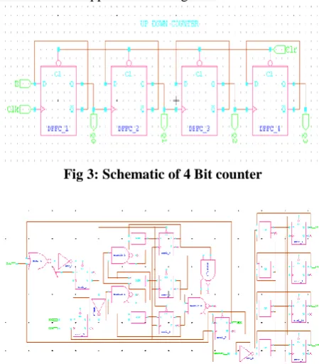
II.III UP/DOWN COUNTER
Successive approximation ADC is the advanced version of Digital ramp type ADC which is designed to reduce the conversion and to increase speed of operation. The major draw of digital ramp ADC is the counter used to produce the digital output will be reset after every sampling interval. The normal counter starts counting from 0 and increments by one LSB in each count, this result in 2N clock pulses to reach its maximum value. In successive approximation ADC the normal counter is replaced with successive approximation register.
Fig 3: Schematic of 4 Bit counter
Fig 5: OpAmp as comparator schematic
Fig 6: OpAmp with push pull amplifier
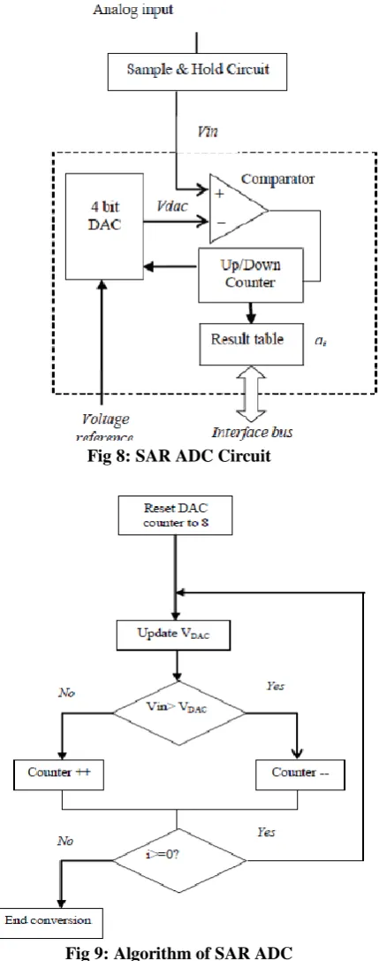
II.V SAR ADC
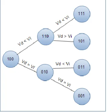
The output of SAR is converted to analog out by the DAC and this analog output is compared with the input analog sampled value in the Opamp comparator. This Opamp provides an high or low clock pulse based on the difference through the logic circuit. In very first case the 3 bit SAR enables its MSB bit as high i.e. „1‟ and the result will be “100”. This digita output is converted to analog value and compared with input sampled voltage (Vin). If the deference is positive i.e. if the sampled input is high then the SAR enables the next bit from MSB and result will be “110”. Now if the output is negative i.e. if the input sampled voltage is less than the SAR resets the last set bit and sets the next bit and resultant output in this case will be “101” which will definitely approximately equal to the input analog value. The counting sequence is explained by the following counter flow chat as shown in below.
Fig 8: SAR ADC Circuit
Fig 9: Algorithm of SAR ADC
The other circuit requirements for the SAR ADC circuit requirements are designed and shown below.
II.V.I OUTPUT SHIFT REGISTER
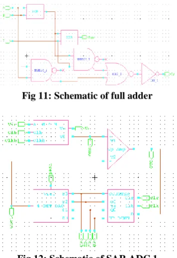
Fig 12: Schematic of SAR ADC 1
III. PROPOSED CIRCUIT
All the above schematic designs were designed using s-edit i.e., schematic editor of Tanner EDA (Electronic Design Automation) tool. Every single circuit was designed using CMOS logic with references from various textbooks. After designing all the schematics for the SAR ADC designs, symbols of those schematics were designed by using the same to reduce the final circuit complexity in connections. Those symbols for their respective schematic designs were above.
After schematic design net-list for all the schematics was generated and simulated in H-Spice to verify the simulated result. It also helps to know the performance characteristics, power leakage values, delay etc.
Fig 13: Schematic of SAR ADC 2
IV. SIMULATED RESULTS 4.1 OUTPUT OF OP-AMP AS COMPARATOR
4.2 OUTPUT OF OP-AMP WITH PUSH PULL
Fig 15: Output of Opamp with push pull
4.3 OUTPUT OF SAMPLE AND HOLD CIRCUIT
Fig 16: Output of S & H circuit
4.4 OUTPUT OF D TO A CONVERTER
Fig 17: Output of D to A Convertor
4.5 OUTPUT OF COUNTER
Fig 18: Output of Counter
4.6 OUTPUT OF UP DOWN COUNTER
Fig 20: Output of SAR ADC 2
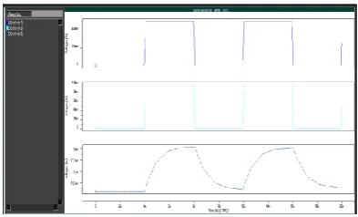
4.8 OUTPUT OF PROPOSED CIRCUIT FOR INPUT OF 0.5V
Fig 21: Output of SAR ADC 1
All the simulated waveforms show the performance of the circuit as the voltage swing is so better. The final circuit was simulated for 0.5V input, which shows all possible internal simulated output waveforms also for better assessment. As there is good voltage swing in the waveforms, we can say that there is no back step in performance scenario.
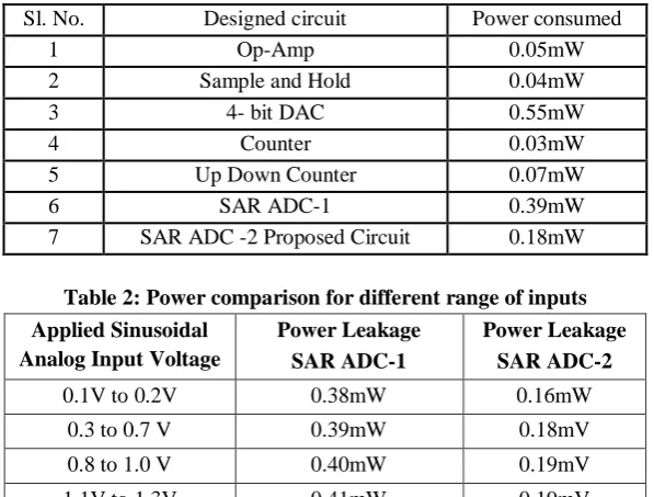
V. POWER CALCULATIONS
In the above table all the power consumption values of individual circuits for different inputs was shown. Finally the combination of all the circuits will lead to SAR ADC, where the power consumption of 0.16mW better than the previous circuit. In this project we can say that by our design power consumption can be further saved better than the previous circuit. Although the ADC has fair accuracy due to 4-bit architecture but it has good resolution on over N over reading for same input values. Also ADC has lower precision but it works good to learn about SAR based ADC design
Table 1: Output power results
Sl. No. Designed circuit Power consumed
1 Op-Amp 0.05mW
2 Sample and Hold 0.04mW
3 4- bit DAC 0.55mW
4 Counter 0.03mW
5 Up Down Counter 0.07mW
6 SAR ADC-1 0.39mW
7 SAR ADC -2 Proposed Circuit 0.18mW
Table 2: Power comparison for different range of inputs Applied Sinusoidal
Analog Input Voltage
Power Leakage SAR ADC-1
Power Leakage SAR ADC-2
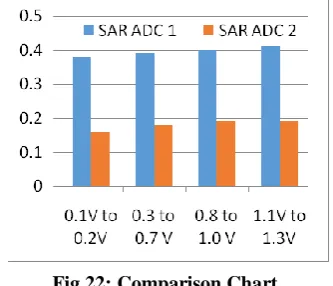
0.1V to 0.2V 0.38mW 0.16mW
0.3 to 0.7 V 0.39mW 0.18mV
0.8 to 1.0 V 0.40mW 0.19mV
.
Fig 22: Comparison Chart
SAR the conversion time is independent of the magnitude of the input sampled value. Advantages of Successive Approximation ADC are speed is high compared to counter type ADC, good ratio of speed to power, compact design compared to Flash Type and it is inexpensive. Disadvantages of Successive Approximation ADC are cost is high because of SAR, complexity in design. Various applications of the SAR ADC will used widely like data acquisition techniques at the sampling rates higher than 10KHz
VI. CONCLUSION
In this paper, structure for up down counter logic and ring counter logic for designing of Successive Approximation Register based ADC. Design logic is simple & easier to design. Although the ADC has fair accuracy due to 4-bit architecture but it has good resolution on over N over reading for same input values. Also ADC has lower precision but it works good to learn about SAR based ADC design.
SAR based ADC will provides us a better solution for various analog to digital systems. It is an essential device whenever data from the analog world, through sensors or transducers, should be digitally processed or when transmitting data between chips through either long-range wireless links or high-speed transmission between chips on the same printed circuit board.
REFERENCES
[1] Hur A. Hussam, Izhal abdul Halin ”Design of 8-bit SAR ADC CMOS” Proceedings of 2009 IEEE Student conference on research and development 16-19 Nov 2009, UPM Serdang, Malaysia.
[2] Ying-zu-lin, chung-cheng liu, Gaun-ying haung, ya-ting shyu, yen-ting liu, soon jyh chang “A 9-bit 150 Ms/s subrange ADC based on SAR architecure in 90-nm CMOS,”IEEE transaction on circuit and systems- I:regular papers, VOL.60, No.3, March 2013.
[3] Anshul Agarwal, Design of Low Power 8-Bit Digital-to-Analog Converter with Good Voltage-Stability, Center for VLSI and Embedded System Technologies International Institute of Information Technology Hyderabad, India May 2013.
[4] Etienne SICARD, CHEN Xi, A PC- based educational tool for CMOS Integrated Circuit Design, INSA, and Department of Electrical & Computer Engineering Av de Rangu
[5] ADC Architecture VII : Counting ADCs by Walt Kester and James Bryant MT – 026 Tutorial
[6] Nilofar M. A. Shaikh , Prof. Seema H. Rajput, Shrikant R. Atkarne - Design of SAR Logic for Low Power High Speed SAR ADC IJAREEIE Vol. 5, Issue 1, January 2016
[7] “Methodology for designing switched capacitor sample and hold circuit used in data converters” IET circuits,Device and systems,28th Nov 2013
[8] Behzad Razavi,”Design of sample and hold amplifiers for high speed low voltage A/D converter”, Custom integrated circuit conference, IEEE 1997.
[9] Specification and architecture of sample and hold amplifier”, National semiconductor corporation,July 1998.. [10] Biao Li,”A high DC gain op-amp for sample and hold circuit”, proceedings of the 2nd international conference
on computer science and electronic engineering, ICCSEE 2013.
[11] Yan Xiang,Fan xiangining ,”Design of sample and hold circuit for a reconfigurable ADC”,International conference on computer science and service system,2012southeast university,Nanjing,China.