February 22, 1999
Mentor Graphics Tutorial
ECE/Comp. Sci. 352 — Digital System
Fundamentals
Charles R. Kime — Department of Electrical and Computer Engineering University of Wisconsin – Madison
Version 299.0
Introduction
This tutorial consists of three parts:
Design Architect – Part 1: Schematic Capture
Design Architect – Part 2: Using Hierarchy and Buses, and QuickSim - Basic Logic Circuit Simulation
During the three parts of this tutorial, you will design a two-way multiplexer, mux2x, combine three such multiplexers to build a four-way multiplexer, mux4x, and perform a logic simulation of mux4x.
In addition, there are four appendices to assist you in using these tools later in the course:
Appendix A: Function Key Shortcuts in Design Architect, Appendix B: Strokes: A Fun Way to Avoid Pushing Buttons, Appendix C: A Word On Flip-flops In Design Architect, and Appendix D: Sample force file mux4_verify.
Notation
Design Architect – Part 1: Schematic Capture
-> Click left mouse button -> A Click left mouse button on A => Double click left mouse button => A Double click left mouse button on A |-> Hold down left mouse button and drag |-> A Hold down left mouse button on A and drag ->^ Drag and release left mouse button
->^ Drag and release left mouse button at A
name Enter text name (followed by RETURN if appropriate) r-> Click right mouse button
r-> A Click right mouse button on A r=> Double click right mouse button r=> A Double click right mouse button on A r|-> Hold down right mouse button and drag r|-> A Hold down right mouse button on A and drag r->^ Drag and release right mouse button
r->^ A Drag and release right mouse button at A
Design Architect – Part 1
:
Schematic Capture
In this lab exercise, you’ll create an a schematic for 2-to-1 multiplexer, a device which selects one of two data inputs to appear at the output. Follow the steps presented on the next several pages to create a schematic for the multiplexer component shown in Figure 1 at the end of the tutorial.
1.Remove the page at the end of the tutorial containing Figures 1 and 2 that you will be copying during the tutorial.
2.Log into your workstation, if you haven’t already done so.
3.Enter mentor_make in your home directory to generate the mgc directory and to add a location map in that directory. If you have done this before this semester, you should repeat it to get the latest version. All of your work with Mentor Graphics tools will be done in mgc or its subdirectories.
4.Close all terminal windows and open two new ones by ->Xterm in the bottom control panel so that these changes take effect.
5.Set up the keyboard so that holding a key will not cause it to repeat that key (Turn the Auto Repeat function off). This is necessary in a few circumstances, such as holding down the F8 key to zoom into an area.
a. -> Style Manager in the bottom control panel (the icon with four items including and artist’s palette and three ‘T’s).
b. -> Keyboard, -> Auto Repeat. Auto Repeat should no longer be depressed or checked. Once you have done this, you may need to turn Autorepeat back on for uses with other tools.
c. -> OK
d. Close the Style Manager window.
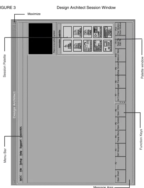
6.Type da at the prompt followed by RETURN. Wait for Design Architect to open. Note the various areas of the initial window called the Session window (see Figure 3).
Design Architect – Part 1: Schematic Capture
FIGURE 3 Design Architect Session Window
7.-> Maximize, the large square button on the upper right hand corner of the window, to make the window as large as possible.
8.Open a new schematic sheet.
a. After the Design Architect Session window is displayed, move the mouse cursor to the Palette window.
b. -> OPEN SHEET. The Open Sheet dialog box appears in the client area.
c. -> Navigator in the Open Sheet dialog box.
This will open a window showing the contents of your default Mentor directory. If this is your first time creating a sheet, then there should be no items in the list for you to select. In the future, however, this is where you may go to open already created sheets. A schematic sheet is represented in the list with a folder icon con-taining a ‘c’ (for component) followed by the name of the component. Clicking on such an item in the list will select it, and clicking on OK automatically places
Session P alette Function K e ys Men u Bar P alette windo w Maximize Message Area
Design Architect – Part 1: Schematic Capture
the name in the Component Name field of the Open Sheet dialog box. Note that double clicking on a component will cause the directory to be opened. Do NOT double click! Click only once to highlight a component and then click OK. You can also click on the arrow buttons to change to different directories, just as you would with the Unix cd command. Next, we want to create a new sheet.
d. -> Cancel in the Navigator window.
e. Complete the entry in the Open Sheet dialog box: $PROJ_PARTS_username/mux2x
where username is your login name. Make sure the cursor is at the end of the line before you enter mux2x. If you make a mistake, click Reset to start again.
f. -> OK on the Open Sheet dialog box to open the sheet.
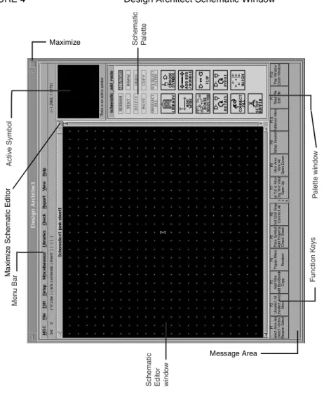
9.-> Maximize, the large button on the upper right of the newly opened Schematic Edi-tor window to maximize its size. Note the various areas of the current window called the Schematic window (see Figure 4).
FIGURE 4 Design Architect Schematic Window
P alette windo w Activ e Symbol Men u Bar
Schematic Editor windo
w Function K e ys Schematic Palette Message Area Maximize Ma x imi z e S c hemat ic E d it or
Design Architect – Part 1: Schematic Capture
10.Now, based on Figure 1, we want to add an instance of a 2-input AND gate to the sheet.
a. Move the mouse cursor to the Palette Menu and -> LIBRARY. The buttons in the Palette Menu disappear and are replaced by a list of gate libraries.
b. -> gen_lib in the list to cause the generic library to appear.
c. r|-> in the Palette Menu and r->^ Show Scroll Bars to add a scroll bar to the list.
d. r|-> and r->^ Set Default Palette. From now on, whenever you click on LIBRARY you will get the list of generic gates.
e. Use the scroll bars or the Page Up and Page Down keys on the right of the key-board to scroll the list until you see the and2 component.
f. -> and2 component.
The Add Instance prompt bar will appear in the lower left hand corner of the Schematic Editor window. Ignore this, since we will be using only default sym-bols. Also, a symbol of a 2-input AND gate will appear in the Active Symbol window.
g. Move the cursor into the Schematic Editor area.
You will see an image of the default symbol for the and2 component.
h. -> when the and2 symbol is about in the center of the Schematic Editor win-dow.
Notice how big the and2 symbol is in the Schematic Editor window. We would like to have more room to place more components, so
11.Zoom out on the sheet by r|-> in one of the scroll bars in the Schematic Editor win-dow, r->^ Zoom Out. This action will shrink the view and allow you to place more components conveniently.
12.Bring back the Schematic Palette using, in the Palette window, r|->, r->^ Display Schematic Palette.
We now want to break from our design process to look at some of the simple, but neces-sary, editing functions used in schematic capture.
13.Selecting and deselecting the and2 instance.
Check to see if the and2 symbol is currently selected; if so, it should look as if it is made up of dashed lines. If it is not selected, then the lines will be solid.
a. Press function key F2. This will deselect and2 (and anything else that is selected). If this does not work, make sure the Schematic Editor window is selected.
b. -> on its outline to select and2.
c. Press F2 again to deselect and2.
d. |-> a box around and2 from upper left to lower right, ->^. This method is very effective for selecting a region of components.
Design Architect – Part 1: Schematic Capture
a. To copy the and2 once, r|-> in the Schematic Editor window and ->^ Copy. Don’t worry about the additional menus indicated by the right arrow after the Copy item; we are only interested in the default copy function.
You will see an and2 symbol in addition to the current one. Move the and2 sym-bol so that the two are not touching and aligned as you desire, and -> to place the gate.
b. To copy the and2 multiple times, -> COPY in the Palette Menu twice and move the cursor back to the Schematic Editor window.
You will see an and2 symbol in addition to the current one. This is actually a “stack” of two and2 symbols. Move the and2 symbol so that the two are not touching, and -> to place the bottom gate from the stack. Move the next and2 symbol that appears to a different location and -> to place that one. The number of and2’s available from the stack is equal to the number of distinct clicks in sequence on COPY before placement is started.
Incidentally, any operation which features a prompt bar or a popup window can be cancelled in the middle of the operation by pressing the ESCAPE key or by -> Cancel in the prompt bar; the result is such that the operation never happens, but any currently selected items remain selected.
c. Delete all but two of the and2 symbols by selecting them and pressing Delete.
15.Moving an and2 instance.
a. Select the and2 symbol that you would like to move.
b. r|-> in the Schematic Editor window and ->^ Move.
c. Position the and2 and -> to cause the old instance to disappear and the new instance to be placed. Notice how similar this operation is to the copy operation.
d. This time, -> MOVE in the Palette Menu and move the cursor back to the Sche-matic Editor window.
e. Position the and2 and -> to cause the old instance to disappear and the new instance to be placed. This will have the same effect as the first method.
16.Delete an and2 instance.
a. Select the and2 to be deleted. Unselect all components first using F2 if neces-sary.
b. r|-> in the Schematic Editor window, r->^ Delete.
17.Undo the previous six steps.
Design Architect has the capacity to remember the last five commands executed, includ-ing selects and unselects.
a. r|-> in the Schematic Editor window, r->^ Undo. Do this three times.
b. -> UNDO button in the Palette Menu three times (this is much easier!).
When you undo for the 6th time, an error message appears in the Message Area at the bottom of the screen stating that the Undo queue is empty. This shows that only five previous commands can be saved.
Since the five commands are still in the queue, it is also possible to redo up to five com-mands. Do redo by r|-> in the Schematic Editor window, r-> Undo, right arrow to Redo r->^ or just, in the Menu bar, -> Edit, -> Redo.
Design Architect – Part 1: Schematic Capture
c. Delete all but one of the and2 symbols.
18.Add another instance of the and2 symbol.
a. Move the cursor to the Active Symbol window and ->.
b. Move the cursor so that the bottom left pin of the instance you are placing is two grid locations (dots) above the top left pin attached to the first and2 instance. (Use the scroll bars or the paging keys on the keyboard to scroll around the sheet if necessary.) You will see the image of the symbol instance.
c. -> when the instance is at the desired location. Refer to the illustration in Figure 1 for the exact location.
19.Add an instance of a 2-input OR to the schematic.
a. -> LIBRARY in the Palette Menu. Notice how the Palette Menu changes directly to the list of gates in the generic library.
b. Use the scroll bar or paging keys on the keyboard to scroll the list until you see the or2 component and -> on the or2 component. The or2 symbol becomes the active symbol and is displayed in the Active Symbol window.
c. Move the mouse cursor so that the left pins of the or2 symbol you are placing are two grid locations to the right of the right pins of the and2 instances.
20.Using the procedures described in previous steps, add an instance of an inverter (NOT gate) inv to the schematic.
Notice that the inv symbol is “pointing” to the right. whereas in the illustration in Fig-ure 1, the inv symbol is pointing up. For now, just place the inv symbol where FigFig-ure 1 indicates.
21.Rotate the inv instance.
a. Use the same procedure as in step 12 to change the Palette Menu from the gate list to the Schematic Palette.
b. Press the F2 (Unselect All) function key to unselect all objects in the Schematic Editor window.
c. Select the inverter instance by -> on its outline.
d. Click on the ROTATE button in the Palette Menu until the inverter looks as if it is pointing upward.
22.Move the inv instance to the correct position.
a. PressF2 (Unselect All) to unselect all objects in the Schematic Editor.
b. -> on the inverter outline to select it.
c. -> MOVE in the Palette Menu.
d. Drag the inverter to the position as shown in Figure 1, and ->.
23.Add input and output ports to the schematic.
a. Using the procedures described in the previous steps, add instances of portin for the inputs and portout for the output.
b. Press F2 to unselect all symbols.
24.Add nets to interconnect the symbols.
a. Display the Schematic Palette in the Palette window.
b. -> ADD WIRE in the Palette Menu. The Add Wire prompt bar appears in the Schematic Editor window, and the cursor changes to a cross.
Design Architect – Part 1: Schematic Capture
c. Move the mouse cursor to a pin vertex and ->. Move the mouse cursor to the next net vertex. If this is a final vertex, =>. If this is an intermediate vertex or point where you want to place a 90 degree bend in the wire, ->.
d. Using these procedures. complete all the nets on the sheet.
e. When you have completed adding nets, press the ESCAPE key, and the cursor will return to normal.
f. Sometimes, when you draw nets, there will be points such as a “T” connection where the nets did not get connected. This will be indicated by a . To connect such points, in the Schematic Palette, -> CONNECT ALL. Also, if you need to delete a net segment just drawn you can use Undo. To select a whole nets for deletion, press F2 and then put the cursor over each net and press F1.
g. Press the F2 (Unselect All) to unselect all objects in the Schematic Editor win-dow.
25.Change net property values.
Note that every instance of the portin and portout symbols has a net name (called NET) attached to it. To prevent the simulator from connecting these together (since they are the same name and hence are the same signal), you need to replace each NET with a unique name. You can change the Net property values of the portin and portout symbol instances in one of two ways:
a. Change property text values one at a time.
Choose the Net property text associated with the portin symbol at the upper left-hand corner of the sheet by positioning the cursor over the property value NET and pressing the Shift-F7 (Change Text Value). This selects the name NET and brings up the Change Property Value prompt bar. Note that this prompt bar also identifies the property name of the text you want to change. Type the following in the prompt bar:
New Value: A
-> OK. The new property value appears in the same location as the NET name. Press the F2 (Unselect All) function key to unselect everything in the window.
b. Change several net values at one time.
Place the cursor over a net (over the wire, not the name NET!) still named NET and press F1 to select the net. Repeat for the nets connected to remaining portin instances and the net connected to the portout instance. Make sure that you only have these nets selected.
r|-> to display the NET popup menu (This menu appears because only nets have been selected), ->^ Name Nets:
This menu item lets you change the net name that is attached to each selected net. The Change Property Value prompt bar is displayed for each net name from the top-most to the bottom-most selected net (without regard to horizontal place-ment).
For this example, the first net name that is highlighted is the net associated with the portout instance. The Change Property Value is displayed. Type in the fol-lowing information:
Design Architect – Part 1: Schematic Capture
-> OK. Another Change Property Value prompt bar is displayed with the mid-dle portin instance. Type in the following information:
New Value: B
Continue changing the net names of all the selected nets in the same manner until you have changed them all.
26.View the entire circuit by pressing SHIFT-F8 (View All).
27.Check the sheet.
a. -> Check -> Sheet -> With Defaults.
A Check Status window will appear in front of the Schematic Editor window which contains a check list. 1f you designed the multiplexer correctly, the win-dow should indicate 0 errors and 0 warnings in all categories.
b. If your check results in errors or warnings, you can identify handle names by clicking the handle name in the Check Status window. The object associated with that handle name is automatically selected on the sheet. Some examples of handle names are: I$2 (for Instances or gates), N$24 (for nets).
c. Close the Check Status window. The Schematic Editor window is automati-cally reactivated.
28.To save the sheet, in the Menu bar, ->File, -> Save Sheet.
The message area displays a message that indicates that the sheet has been saved.
29.Print the sheet.
Before printing the sheet, it is necessary to set up the printer to be used:
a. -> MGC -> Setup -> Printer
b. Select the desired printer or postscript format. We will select (highlight) bw_PS_file, (black and white postscript) since we do not want to actually send the file to a printer. -> Select Printer; bw_PS_file should appear in the Selected Printer area. -> OK.
Postscript files will appear in the /tmp directory on your workstation; save them somewhere else before you log off if you want to keep them! The file can be printed using CAE print commands or sent by ftp elsewhere for printing. Note that ordinarily you are likely to be printing directly to a printer rather than a post-script file.
c. In the Menu bar, ->File, ->Print Sheet. A prompt bar will appear in the lower left hand corner of the screen. -> OK
d. To view the postscript file, in a terminal window (you may need to bring up a new one), enter cd /tmp. Then enter ls and look in the list for a
file_name containing your username and a .ps extension. Then enter gv file_name to view the printout.
30.Close the Schematic Editor. If you made any changes since the last save, then you will be asked if you wish to save the sheet again.
Design Architect – Part 2: Using Hierarchy and Buses
Design Architect – Part 2
:
Using Hierarchy and Buses
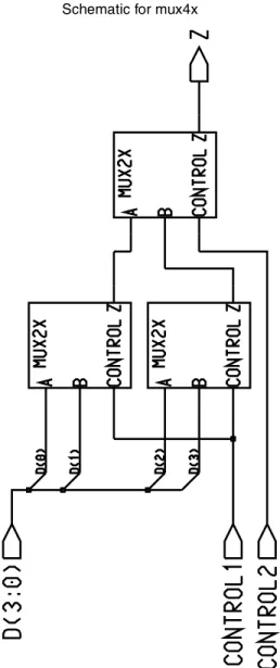
In this lab exercise. you will first create a symbol for the 2-to-1 multiplexer, mux2x, that you already created so that you can use it as a part in another design, like any other part in the library. Then, you will create the sheet for a 4-to-1 multiplexer using the 2-to-1 multiplexer module created earlier. The sheet for the 4-to-1 multiplexer is shown in Fig-ure 2.
1.If you are not currently logged into a workstation, log in and turn off autorepeat as done in Part 1.
2.If you are not already in da, enter da at the prompt and press RETURN.
3.When the Design Architect Session window appears, -> Maximize.
4.Open the schematic for the 2-to-1 multiplexer, mux2x.
a. In the Palette Menu, -> OPEN SHEET.
b. -> Navigator in the Open Sheet dialog box.
This will open a window showing the contents of your default mgc directory.
c. Select mux2x, and -> OK.
d. -> OK in the Open Sheet dialog box.
WARNING! Do not touch any other entries on the Open Sheet dialog box! Particularly do not mess with sheet 1!
5.Create a symbol for the 2-to-1 multiplexer, mux2x.
a. In the Menu bar, -> Miscellaneous, -> Create Symbol. The Create Symbol dia-log box appears in the client area.
b. -> Yes for Replace, Save then edit? and Sort Pins?,-> OK.
WARNING! Do not touch any other entries on the Create Symbol dialog box!
A new window appears containing a drawing of a box with the inputs to the mul-tiplexer on the left side and the output on the right side. This is the default shape that Design Architect creates for symbols of schematics.
6.Add a reference label to the symbol.
c. Select the symbol box by clicking on its outline.
d. In the Schematic Editor window, r|-> Properties -> Add -> Add Single Prop-erty r->^. The Add PropProp-erty dialog box appears.
e. In the list area in Add Property, -> REF and then enter MUX2X and -> OK.
f. Move the cursor to the upper portion of the symbol, placing MUX2X to the right of A.
g. In the Menu bar, -> Check, -> With Defaults.
h. In the Menu bar -> File, -> Save Symbol.
i. Close the Symbol Editor window.
Now that we have created a symbol for the 2-to-l multiplexer. we can use it as a compo-nent to build a 4-to-1 multiplexer. See Figure 2.
Design Architect – Part 2: Using Hierarchy and Buses
1.Open a new schematic sheet.
a. In the Palette Menu, -> OPEN SHEET.
b. Edit the Component Name to: $PROJ_PARTS_username/mux4x
c. -> OK.
d. -> Maximize in the Schematic Editor window (not the Design Architect Ses-sion window) to make the window as large as possible.
2.Add an instance of mux2x to the sheet
a. In the Palette window, -> CHOOSE SYMBOL. The Add Instance/Choose Symbol dialog box appears in the client area. Notice that the mux4x component appears in the list in addition to the mux2x component. It cannot be used since it has no symbol and using it would be recursive!
b. Highlight mux2x and -> OK.
The Add In prompt bar will appear in the lower left hand corner of the Sche-matic Editor window. Also, a symbol of a 2-to-l multiplexer will appear in the Active Symbol window.
c. Move the cursor into the Schematic Editor window. An image of the default symbol for mux2x appears.
d. -> when the mux2x symbol is about in the center of the Schematic Editor win-dow.
Notice how big the mux2x symbol is in the Schematic Editor window. We would like to have more room to place more components, so...
3.r|-> Zoom Out in one of the scroll bars in the Schematic Editor window to enlarge the view.
4.Add a second and third instance of mux2x.
a. Move the cursor to the Active Symbol window and ->.
b. Move the mouse cursor with the mux2x image attached so that the bottom left pin of the instance you are placing is 3 grid locations (dots) above the top left pin attached to the first mux2x.
c. Repeat a and b, except this time, place the multiplexer so that the CONTROL pin is 1 grid point up and 3 grid points to the right of the Z pin in the bottom most instance.
5.Add input and output ports to the schematic.
Using the procedures described in the basic Design Architect tutorial, add instances of the portin and portout symbols to your schematic sheet where needed. Recall that these can be found in the generic library, gen_lib.
6.Add a bus to the schematic.
A bus in Mentor Graphics is a bundle of nets or wires. To illustrate the bus concept, we will use a 4-bit bus instead of four individual wires for our data inputs which we will call D(3), D(2), D(1), D(0). The bus will be called D(3:0). In this case, the bus is attached to a portin as shown in Figure 2.
a. In the Schematic Palette, -> ADD BUS BUNDLE. A Prompt bar will appear and the cursor with change to a cross just as it does for a wire. Drawing a bus is just like drawing a wire.
Design Architect – Part 2: Using Hierarchy and Buses
b. |-> on the output of the upper portin and draw the bus down to the point where the 45 degree angle goes to D(0), =>.
c. Press ESCAPE to cancel further bus drawing.
d. In the Schematic Editor window, r|->, ->^ Name Nets:
e. In the Prompt bar that appears, enter D(3:0) in the Property Value area.
f. Using the cursor, place the D(3:0) that appears in the Schematic Editor window to the left of the portin for the bus.
g. Press F2 to deselect all objects.
If we had a component with a portin attached to a 4-bit bus t with corresponding num-bering inside it, our bus could be attached to the corresponding input pin on the compo-nent symbol. But in our case, the data inputs to the two mux2x compocompo-nents to which the bus is to be attached are four single nets. In such a case, we have to “rip apart” the bus to make the connections. The wires we generate in the process are attached to diagonal segments on the bus called “rippers.” Fortunately, the rippers are generated automati-cally, but we do need to fill in the ripper labels to specify exactly how the bus nets are connected to the mux2x components.
7.Attach the A and B input ports on two mux2x symbols to the bus D(3:0).
a. In the Schematic Palette, -> ADD WIRE.
The Add Wire prompt bar appears in the Schematic Editor window and the cur-sor changes to a cross.
b. Place the cursor on the A pin on the top mux2x. |-> to the bus and =>.
The ripper will automatically appear on the bus and a Choose Bit dialog box will appear.
c. In the Bit area in the dialog box enter 0. The label D(0) appears on the ripper.
d. Repeat a through c for the other three mux2x inputs as shown in Figure 2, enter-ing the appropriate integer, 1, 2 or 3, to label the rippers.
e. When you have completed adding nets, press ESCAPE to cancel Add Wires.
f. Press the F2 to unselect all objects in the Schematic Editor window.
8.Add all remaining nets in Figure 2 using techniques from Part 1 of the tutorial.
9.Change all NET values to the appropriate input and output labels using the techniques from Part 1 of the tutorial.
Note that due to the hierarchical structure, the net names can be the same, e. g., Z, as those used for mux2x.
10.View the entire circuit by pressing SHIFT-F8 (View All). This is important at this point to determine if there are any components or wires floating around that you might have accidentally added. Press F2 to deselect all objects in the Schematic Edi-tor window.
11.In the Menu bar, |-> Check -> Sheet ->^ With Defaults to check the sheet.
12.If there are errors, use techniques in Part 1 of the tutorial to locate them. If there are warnings, it is recommended that you save the sheet and check it again to see if they disappear.
QUICKSIM – Basic Logic Simulation
14.Print the sheet to a postscript file using the techniques given in Part 1 of the tutorial.
15.Close the Schematic Editor window. If you made any changes since the last save, then you will be asked if you wish to save the sheet again.
16.Exit Design Architect by closing the outmost window.
QUICKSIM – Basic Logic Simulation
Now that you have created the 4-to-1 multiplexer, you can use QuickSim II to simulate the design.
1.Enter quicksim mux4x at the prompt.
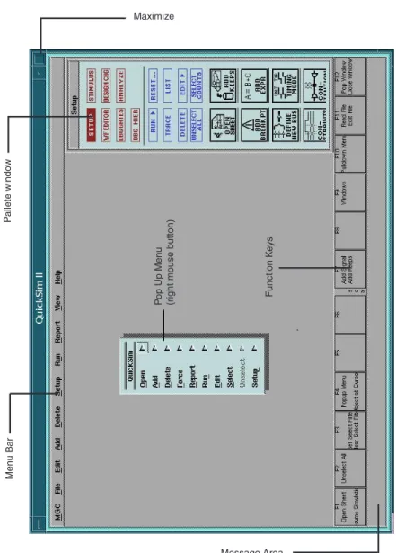
The QuickSim II window appears as in Figure 5. This figure will be used frequently for tool references.
2.-> Maximize to get the QuickSim Il window to fill the entire screen.
3.In the Setup Palette window, -> Open Sheet to view the schematic sheet for mux4x.
4.Select all of the named nets in the mux4x schematic view window.
In this step, and the subsequent steps, you perform selection on signals in the Sche-matic View window. You will create the List and Trace windows which include the selected signals.
Select each named net in the design. This is best done by a -> on each portin and portout symbol or carefully using a box to select all portins and a box to select all portouts.
If you make a mistake and select the wrong items (like internal nets), -> on the object you selected by mistake. Object selection toggles. Note that for debugging purposes, you may select internal nets as well.
5.In the Setup Palette, ->Trace to open the Trace window containing the selected sig-nals.
The Trace window displays waveforms of signal activity. Signal names appear along the left edge of the Trace window. Because the signals are selected, the names should be highlighted (in yel1ow). Along the bottom of the Trace window are time labels in 100 nanosecond increments which are marked by columns of tic marks (+).
A row of tic marks identifies the logic level of a signal according to the following rules:
A trace drawn through the tic marks: an unknown (X) logic value. Unknown logic values can be either 0 or 1. but it is uncertain which they are.
A trace drawn above the tic mark: a high (1) logic value. A trace drawn below the tic mark: a low (0) logic value.
6.In the Setup Palette, -> List to open the List window.
The List window displays a tabular listing of signal activity. It can display signal val-ues in binary, octal. decimal, or hexadecimal, whichever is the default.
QUICKSIM – Basic Logic Simulation
FIGURE 5 QuickSim II Window
The signal names appear at the bottom of the list window. The up-arrow that accom-panies each signal name points to the column that will contain the state values for the signal. The initial signal values appear at the top of the List window. If the value of a listed signal changes, the value is highlighted (or appears in green on color monitors). Before unselecting anything, note that the signal names are highlighted in both the Trace and List windows. These signals are selected, so all windows show them selected.
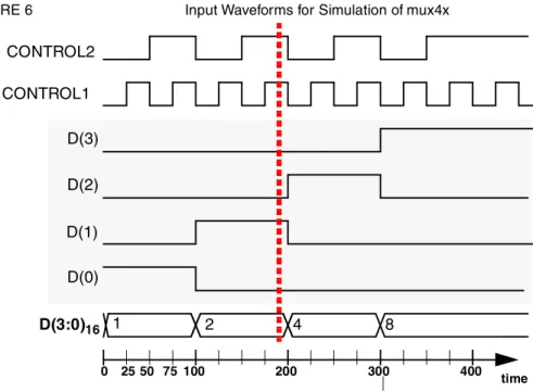
7.Press F2 to unselect all signals. You can also unselect individual signals if you like. Next, we want to apply inputs to the mux4x to test it. The input waveforms to be applied are given in Figure 6. We will apply the inputs to the left of the dotted vertical line only for now. Men u Bar P allete windo w P op Up Men u (r ight mouse b utton) Function K e ys Maximize Message Area
QUICKSIM – Basic Logic Simulation
FIGURE 6 Input Waveforms for Simulation of mux4x
The first type of stimulus we will use is “manual” force, where the user tells the simula-tor the value to change to and the time to do the change.
8.Apply forces to the CONTROL2 input.
a. -> CONTROL2 in the TRACE or LIST windows to select it.
b. In the Setup Palette, -> Stimulus, ->Add Force.
The simulator displays the Force Multiple Values dialog box. Note that this function allows you to specify different values at different times on a signal.
c. In the dialog area labeled Value, type 0 followed by TAB.
d. Next type (in the dialog area labeled Time), type 0 followed by TAB.
e. Continue entering Values and Times: 1, 50, 0, 100, 1, 150, following each entry with TAB.
f. Move the cursor to the bottom of the Force Multiple Values dialog box and -> OK.
The second type is an “automatic” force, more commonly referred to as a clock signal or a periodic waveform. This will be discussed later.
9.Apply a clock (periodic waveform) to the CONTROL1 input.
a. -> CONTROL2 in the TRACE or LIST windows to deselect it.
b. -> CONTROL1 in the TRACE or LIST windows to select it.
c. In the Palette window, -> Add Clock.
d. In Force a Clock Signal, type 50 in Period, specifying a clock with a period of 50.
e. Note that the Duty Cycle is 50% meaning the clock is at 1 or 50% of the time or for 25 time intervals. This is what we want. Other values should be left at the default. CONTROL1 CONTROL2 D(3) D(2) D(1) D(0) D(3:0)16 1 2 4 8 time 0 25 50 75 100 200 300 400
QUICKSIM – Basic Logic Simulation
f. -> OK to enter the clock signal.
10.Apply forces to the bus D(3:0).
Note that these forces in Figure 6 are converted to hexadecimal since D is a 4-bit bus. If D had more or fewer bits, multiple hexadecimal values could be used. The hexadec-imal number will be right justified if the number of bits is not divisible by four.
a. -> CONTROL1 in the TRACE or LIST windows to deselect it.
b. -> D(3;0) in the TRACE or LIST windows to select i
c. In the Palette window, ->Add Force.
The simulator displays the Force Multiple Values dialog box. Note that this function allows you to specify different values at different times on a signal.
d. In the dialog area labeled Value, type 1 followed by TAB.
e. Next type (in the dialog area labeled Time), type 0 followed by TAB.
f. Continue entering Value and Time: 2, 100, following each entry with TAB.
g. Move the cursor to the bottom of the Force Multiple Values dialog box and -> OK.
11.Now run the simulation for 200 nanoseconds.
a. In the Palette window, -> RUN, -> For Time.
b. A prompt labeled Run Simulation will appear. In the For Time area, type 200 and -> OK. The simulation results will appear in the TRACE and LIST win-dows.
c. Expand the signals to fill the entire TRACE window by pressing SHIFT-F8.
d. Examine the signals in the TRACE window. Note that they are solid blue and lie either above (1) or below (0) the tic marks for the most part. If a signal lies at the level of the tic marks, as Z does near 0 time, the signal is of unknown value. The reason Z is unknown is due to the delay of the gates between the inputs and out-put Z. The values applied at time 0 require several gate delays to produce a known output value at Z.
e. Examine the signals in the LIST window. Signal values that have “changed” from the prior entry in the list are in green. Note that the Z signal is X (unknown) until 0.5 ns into the simulation. For the simulations that you will be doing, each gate has a delay of 0.1 nanoseconds from the change in the input to the change in the output. (More realistic simulation have different gate delays for each gate depending on its type and possibly the load on its output.) For this reason, it is best not to make two changes in any signal in an interval of time shorter than the longest total delay in your circuit, which, for equal gate delays, is equivalent to the largest number of gates through which a signal has to travel.
12.Now run the simulation for 200 more nanoseconds.
a. In the Palette window, -> RUN, -> For Time.
b. A prompt labeled Run Simulation will appear. In the For Time area, type 200 and -> OK. The simulation results will appear in the TRACE and LIST win-dows.
Note that the simulation continues from 200 ns to 400 ns using the forces we entered.
QUICKSIM – Basic Logic Simulation
a. To reset the simulator to start over at 0 ns, in the Palette window, -> Reset. The simulator displays the Reset dialog box, which enables you to reset three areas of the simulator at one time: the state, the Sim View setup, and the Quick-Sim setup. In this exercise, you want to reset only the state. which is the button at the top of the dialog box.
b. -> State and -> Save “results” Waveform DB so that it is not active, -> OK. Notice that the traces and values in the windows are removed.
14.Run the simulation one more time for 200 ns.
15.Print the simulation results.
The only two windows that you can print in QuickSim II are the List and Trace win-dows. Before printing these, printing must be set up. Before printing the sheet, it is necessary to set up the printer to be used:
a. -> MGC -> Setup -> Printer
b. Select the desired printer or postscript format. We will select (highlight) bw_PS_file, (black and white postscript) since we do not want to actually send the file to a printer. -> Select Printer; bw_PS_file should appear in the Selected Printer area. -> OK.
Postscript files will appear in the /tmp directory on your workstation; save them somewhere else before you log off if you want to keep them! The file can be printed using CAE print commands or sent by ftp elsewhere for printing. Note that ordinarily you are likely to be printing directly to a printer rather than a post-script file.
c. -> in the Trace window to select it for printing.
d. In the Menu bar, ->File, ->Print Sheet. A prompt bar will appear in the lower left hand corner of the screen. -> OK
e. To view the postscript file, in a terminal window (you may need to bring up a new one), enter cd /tmp. Then enter ls and look in the list for a
file_name containing your username that looks like a trace file and a .ps extension. Then enter gv file_name to view the printout.
16.The List window can also be printed, but it is probably better to just save the results to an ASCII file and print the file, since the data in the List window is just text any-way.
a. Select the List window.
b. In the Menu bar, ->File,->Write
c. The Write Report dialog box appears. In Pathname, enter mux4_list. If you want to place the resulting file anywhere but /mgc, you will need to use the Nav-igator. Buttons allow you to replace the file if it already exists or append the cur-rent results to the already existing file. If you want to mark changes with an *, -> Show in Highlights.
d. -> OK.
e. In another terminal window, use a Unix editor to view the file you wrote. Next we want to further examine options for simulation inputs, i. e., forces.
17.Suppose you want to save the forces you have been using during the simulation for future use.
For More Information
a. To save the forces ->File -> Save ->WaveformDB.
b. The Save Waveform DB dialog window will appear. -> forces, enter mux4_forces in the Pathname area, and -> Forcefile.
c. Enter the time you want the forces to end in Stop Time, e.g., 200 and ->OK.
d. Reset the simulator back to 0 ns again.
18.Delete forces so that the loading of forces can be demonstrated.
a. To delete all forces, in the Palette window, -> Delete Forces.
b. The Delete Forces dialog box appears. The three buttons allow you to delete the forces on any selected signals, any signals which the user names, or all signals. -> All Signals, -> OK.
19.Suppose you want to use the force file that you saved. If you have not set up the Trace window and/or List windows, do that first. Since we already have those set up, we can proceed to load the saved force file.
a. To load force file mux4_forces, |->Setup, ->Force,->^From File.
b. In the Pathname area, enter mux4_forces.
c. Run the simulation for 200 ns to see if the file was loaded.
d. Reset the simulation and delete all forces.
e. Close the Trace window.
20.Another option is to write a force file by hand and load it. To do a more complete simulation of mux4x for verification purposes, we have entered a force file for you which we will now load. This force file also contains information to automatically set up the Trace window and run the simulation. The file is given at the end of this tuto-rial in Appendix D.
a. In a terminal window, enter in your mgc directory,
cp ~ece352/public_html/force_files/mux4_verify . (Do type this . ; it is not a period!)
b. ->Setup, ->Force, ->From File.
c. A Load Forcefile dialog box appears. Navigate to mux4_verify.
Due to the commands in this force file, the simulation will run automatically!
21.Close the QuickSim II window. A dialog box will appear asking you if you wish to save any results. -> Without Saving, ->OK.
For More Information
For on-line help, enter bold_browser followed by RETURN. Look for manuals for Design Architect or Quicksim. Use the Search feature.
Acknowledgments
Acknowledgments
The efforts of Timothy Lambert in writing the prior tutorial on which this one is heavily based are gratefully acknowledged. Fahad Ahmad and Ed Brann also offered a number of helpful suggestions for improvement and contributed to the initial testing of the tuto-rial. Also, Fahad provided the force file in Appendix D.
Appendix A
:
Function Key Shortcuts in Design
Architect
The following is a list of function key shortcuts that are useful in Design Architect. For more information (and more shortcuts) please consult the document Design Creation Quick Reference Guide Booklet using bold_browser.
FUNCTION KEY ALONE:
Fl SELECT AREA ANY - Selects all objects in a given area regardless of the selection filter.
F2UNSELECT ALL - Unselects all selected objects regardless of the selection filter. F3 ADD WIRE - Creates single bit wire segments between points. Click mouse button at initial and intermediate points. Double-click to end wire.
F4 POPUP MENU - Displays popup menu for active window. To select menu items, enter the underlined letter in the menu item desired. This lets you use popup menus without using the mouse.
F5 PLACE SYMBOL - Places the current active symbol at the specified location. F6 SET GRID SNAP -
F7 SELECT TEXT & MOVE - Selects the text under the cursor and drags to new loca-tion.
F8 VIEW AREA - Scales window to rectangle defined during down/up stroke. Hold down the F8 key, draw the desired box with the Select (left) button, and release the F8 key. Note that this can also be accomplished without the F8 key simply by using the middle mouse button instead of the left mouse button.
F9 SETUP SESSION - Opens the Setup Session dialog box~ so you can modify the input device, window layout, and visible areas within the Session window.
F10 PULLDOWN MENU - Selects the first menu bar button. To select menu items, enter the underlined letter in the menu item desired. This lets you use pulldown menus without using the mouse.
ESC(APE) CANCEL - Cancels an open dialog box or a prompt bar. RETURN EXECUTE - Executes an open dialog box or prompt bar. SHIFT + FUNCTION KEY:
Strokes: A Fun Way to Avoid Pushing Buttons
Fl SELECT VERTEX - Selects vertices of objects in a given area.
F2 UNSELECT AREA ANY - Unselects the objects within a given area, regardless of the selection filter.
F3 ADD BUS - Creates multi-bit net segments between points. Click mouse button at initial and intermediate points. Double click to end bus.
F4 (nothing)
F5 ADD PROPERTY - Adds the given property name/value pair to selected electrical symbol and comment objects.
F6 CONNECT ALL - Connects net segments and pins that are in contact but not con-nected.
F7 CHANGE TEXT VALUE - Sets up the change of the text value of a property or com-ment under the cursor location.
F8 VIEW ALL - Scales window at pointer location to display all information. F9(nothing)
F10 (nothing)
CONTROL + FUNCTION KEY:
F1 REOPEN SELECT - Opens a closed selection set.
F2 MOVE - Moves selected electrical or comment objects to the cursor location. F3 COPY - Copies selected electrical or comment objects to the cursor location. F4 RESELECT - Reselects the previous selection set.
F5 CHECK SHEET - Performs error checking on the sheet.
F6 CONNECT ALL - Connects net segments and pins that are in contact but not con-nected.
F7 OPEN UP - Opens the sheet(s) hierarchically above the instance under the cursor. F8 OPEN DOWN - Opens the sheet(s) hierarchically below the instance under the cur-sor.
F9(nothing) F10(nothing)
Strokes: A Fun Way to Avoid Pushing Buttons
By holding down the center mouse button and drawing simple, intuitive graphics in the Schematic Editor window, you can execute many of the Mentor Graphics commands. Since this method is mistake prone, you must use it with caution and be sure to remem-ber UNDO!
1.To experiment with strokes, open a new sheet and place a few components in the sheet.
Appendix C: A Word On Flip-flops In Design Architect
2.Hold down the center mouse button and draw (? minus the .) to display the strokes for the various commands. This information is also given in Figure 7.
3.Select a component and try some of the stroke commands such as Copy and Move. Note the Copy stroke is letter C drawn in the normal direction and the Move stroke is the first two “strokes” of the letter M.
FIGURE 7 Quick Guide to Strokes
Appendix C: A Word On Flip-flops In Design
Architect
In Design Architect (da), you will be using flip-flops to design sequential circuits for projects. The difference between those typically used in the text and those in the genlib library in da is the addition of two extra inputs called preset and clear. These inputs allow you to set the flip-flop to either a 0 (using the clear) or a 1 (using the preset) with-out a positive edge on the clock. They are the same as the S and R inputs in Figure 4-16 in the text and are asynchronous inputs meaning that they affect the output value
Appendix C: A Word On Flip-flops In Design Architect
diately, rather than at the next positive clock edge. For example. if you were to apply a control signal to the preset input, the value of the Q output would change to a 1 right away. Also because the signals are asynchronous. you can for example hold the preset input at the control value and the Q output will remain at 1 no matter what you try to clock into the regular inputs. The same rules apply for the clear input, except that the Q output will change to 0 immediately and remain at 0 for as long as the clear input is con-trolled. Note that the QB (Q) output will always be the inverse of whatever the Q value is at any time.
It is for this reason that the preset and clear inputs must be set to non-controlling values during normal operation of the flip-flops in a sequential circuit. In the D-flip-flop dia-gram shown in Figure 8, we can see that there are “bubbles” on the preset and clear inputs, indicating that the preset and clear actions occur in response to an applied 0. Applying a 1 to these inputs will cause the flip-flop to be unaffected. Thus in normal operation, these inputs should at logic 1. In genlib, logic 1 is provided by the component vcc which is the power supply vcc.
FIGURE 8 gen_lib D Flip-Flop
It turns out, however, that these inputs are of use in designing and simulating sequential logic circuits. The state of the flip-flops is typically unknown when the power is turned on. In some cases, this may be acceptable, but often at least some of the flip-flops need to be initialized to a known state for the circuit to function correctly. Likewise, if the state of a system becomes messed up (as when a computer locks up), it is desirable to have a way to get it back to a known state again. Both of these cases can be handled by providing an asynchronous RESET_B input that is connected to those flip-flops needing it. For power-up, the RESET_B is driven by a circuit that applies a 0 to it for a short interval after the power is applied and then changes to 1. For system reset at other than power up, RESET_B is driven by a pushbutton that applies a 0 when depress and applies a 1 otherwise. So that both of these signals can be applied, they are fed to an AND gate with its output tied to RESET_B. When you are designing a circuit in this course, you can assume that RESET_B is an input to your circuit and ignore this attached circuitry. Typically, those flip-flops that are to be initialized are reset to 0. Thus, the RESET_B signal is attached to the Clear inputs on the flip-flops and VCC is attached to the Preset inputs. In this situation, shown in Figure 9, the desired initial state of the circuit should
Appendix D: Example Force File - mux4x_verify
be the all-0 state. In some cases, we want one or more of the flip-flops to be initialized to 1. For these flip-flops, we connect RESET_B to Preset and VCC to Clear.
FIGURE 9 Typical Asynchronous Power Up Reset Connections
It should be noted that some designers use the Preset and Clear inputs during normal, non-reset operation of logic circuits. This results in circuits that have asynchronous events occurring and unless absolutely essential to get the proper circuit behavior should be avoided since they can lead to insidious circuit malfunction. In this class, the circuits are to be fully synchronous and such use of Clear and Preset inputs is not permitted.
Appendix D: Example Force File - mux4x_verify
This shows the manually-written force file used in the tutorial. The file is heavily com-mented and can provide a guide for writing your own force files.
// A sample force file, mux4_verify, for quicksim // For a 4x1 Multiplexer (See Figure 2)
// Note:- All time units are in nanoseconds // These two statements reset all states and // delete all current forces
$$reset_state();
$$delete_forces(@all, void);
// The following statement to delete the specified traces, // i.e. for the inputs on D(3:0), and the two control signals // CONTROL1 and CONTROL2
Appendix D: Example Force File - mux4x_verify
// This statement adds traces for the specified // signals viz. D(3:0), CONTROL1 and CONTROL2
add traces D(3:0) D(0) D(1) D(2) D(3) CONTROL1 CONTROL2 Z // Force the named signal, D(3:0) to a specified value // in the specified interval. In case the signal is on a // bus, a hex value must be specified. Here, the signal // D(3:0) takes on the value 0x1 (4-bit binary 0001) // between t=0 and t=100.
// D(3:0) = 0x2 from t=100 to t=200 // D(3:0) = 0x4 from t=200 to t=300 // D(3:0) = 0x8 from t=300 to t=400
// If no end time is mentioned, the last force value // holds until the end of the simulation.
force D(3:0) 1 0 100 -fixed force D(3:0) 2 100 200 -fixed force D(3:0) 4 200 300 -fixed force D(3:0) 8 300 400 -fixed
// CONTROL2 is a 1-bit signal that can take on the values // 0 and 1. CONTROL2 = 0 from t=0 to t=50
// CONTROL2 = 1 from t=50 to t=100 // CONTROL2 = 0 from t=100 to t=150 // CONTROL2 = 1 from t=150 to t=200 // CONTROL2 = 0 from t=200 to t=250 // CONTROL2 = 1 from t=250 to t=300 // CONTROL2 = 0 from t=300 to t=350
// CONTROL2 = 1 from t=350 till end of simulation force CONTROL2 0 0 50 -fixed
force CONTROL2 1 50 100 -fixed force CONTROL2 0 100 150 -fixed force CONTROL2 1 150 200 -fixed force CONTROL2 0 200 250 -fixed force CONTROL2 1 250 300 -fixed force CONTROL2 0 300 350 -fixed force CONTROL2 1 350 -fixed
// CONTROL1 is also a 1-bit signal that can take on values 0 & 1 // However, we treat it differently from CONTROL2 to demonstrate // the usage of clocks. We treat CONTROL1 as a clock with period // of 50 nanoseconds.
set clock period 50
force CONTROL1 0 0 -repeat force CONTROL1 1 25 -repeat
//Run the simulation for 400 nanoseconds run 400
Mentor Graphics Schematics Sheets
Mentor Graphics Schematics Sheets
Mentor Graphics Schematics Sheets