Self-Consistent Analysis of Barrier Characterization
Effects on Quantum Well Laser Internal Performance
Zahra Danesh Kaftrouddia and Abolfazl Mazandaranib
aDepartment of Engineering Sciences, Faculty of Technology and Engineering East of Guilan, University of Guilan, Rudsar-Vajargah, Iran
bPlasma & Nuclear Fusion Research School, Nuclear Science & Technology Research Institute, Tehran, Iran
Corresponding author Email: [email protected]
Received: Nov. 1, 2017, Revised: Feb. 26, 2018, Accepted: Apr. 30, 2018, Available Online: June. 30, 2019 DOI: 10.29252/ijop.13.1.23
ABSTRACT— In this paper, a numerical study of barrier characterization effects on the high-temperature internal performance of an InGaAsP multi-quantum well laser is presented. The softwareused for this purpose self-consistently combines the three-dimensional simulation of carrier transports, self-heating, and optical waveguiding. The laser model calculates all relevant physical mechanisms, including their dependence on temperature and local carrier density. The results have shown that the proposed laser, which operates at 1325 nm, suffers from electron leakage. The electron leakage current decreases by reducing the barrier thickness. Although tensile strain barriers lead to improved laser optical behavior, it increases leakage current because of electron non-uniformity.
KEYWORDS: Multi Quantum well, Barrier, Simulation, Leakage, PICS3D, Vertical Current density.
I.
I
NTRODUCTIONQuantum-well (QW) active semiconductor lasers enjoy widespread commercial use in optoelectronic applications ranging from a high power sources for medical therapy, material processing, laser printing, and pumps for solid-state lasers to lower output power single mode and single frequency sources for telecommunications. The advent of highly controllable semiconductor growth technologies led to device quality, nearly ideal
QW materials in the 1980s. Since then, there have been continuous improvements in QW-based device performance. QW lasers, such as InGaAsP/InP, have become the workhorse material for optical fiber sources [1].
When designing long wavelength laser diodes, one important step is to carefully choose a proper waveguide structure, which is capable of achieving minimal internal loss and maximal internal quantum efficiency .It was recognized that the use of compressively strained quantum-wells is required to achieve these goals due to the lower transparency and higher differential gain provided by such active regions. In addition, strained QWs were reported to reduce losses related to Auger-recombination and intervalence band absorption. Strained InGaAsP QWs on InP substrates is the most established and well-investigated material system employed in long wavelength semiconductor lasers. The number of QWs based on this material system has always been large (5-15) due to difficulties in fabricating low loss optical cavities and due to QW gain saturation and excessive carrier losses at higher carrier concentrations and temperature. Compressively strained QWs and strain values in the order of 1% are commonly used in long wavelength QW lasers [2].
The optical performance of the MQW in the active region of an injection laser depends upon many factors. Vertical carrier injection of
carriers through the MQW hetero-junctions is an important consideration when designing the active region. The QW depth or the barrier bandgap should not be too high if a fast carrier injection is desired from the p-doped cladding region to the MQW. Thus, the barrier characterizations must be regarded as one of the most important parameters in the laser design [3].
Simulation is a very helpful and valuable work tool in manufacturing. It can be used in the industrial field allowing the system’s behavior to be learned and tested. Simulation provides a low cost, secure, and fast analysis tool. It also provides benefits that can be achieved with many different system configurations [4]. In this study, first, we will simulate typical InGaAsP-InP multi-quantum well laser with lattice match barriers using Photonic Integrated Circuit Simulator in 3D (PICS3D), which self-consistently combines 3D simulation of carrier transport, self-heating, and optical wave-guiding; then, the same structure will be investigated with different barrier characterizations.
In Sections II and III, we introduce the device structure and theoretical models and in Section IV, we discuss and present the simulation results.
II.
D
EVICES
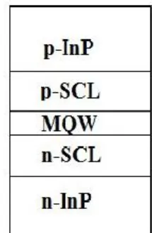
TRUCTUREThe simulation example in this article is a typical InGaAsP multi-quantum well laser diode grown on InP. Figure 1 presents the studied structure. MQW active region consists of six 6-nm thick 1.2% compressively strained InGaAsP quantum wells. The large compressive strain is preferred for reducing the threshold and increasing the gain coefficient. The 10 nm thick barriers exhibit no strain. For the given wells, the barrier thickness is selected as 10nm to avoid any bounded state coupling among different wells. The MQW stack is sandwiched between a pair of un-doped170 nm-thick lattice matched with InGaAsP separate confinement layer (SCLs),
which act as a waveguide. Above and below the active region, heavily doped p and n-type (2×1018 cm-3) InP cladding layers are used to improve electrical current injection. A highly doped p-InP contact layer is employed to complete the entire laser structure. The Fabry-Perot resonator length is considered to be 500 μm. Both laser facets are given a reflectivity 32%.
Fig. 1. The structure of the studied laser.
The layer composition, doping level, and thickness for each of the layers in the laser structure are given in Table 1.
Table 1. The epitaxial layer structure
Layer Doping
(cm-3)
Thickness (10-4cm) n-InP (substrate) 2×10¹⁸ 40 InP ( n- cladding) 2×10¹⁸ 1.3 i-In0.87Ga0.13As0.28P0.72(n-SCL) Un-doped 0.17 i-In0.87Ga0.13As0.28P0.72(Barrie×7) Un-doped 0.01 i-In0.936Ga0.064As0.51P0.49(QW×6) Un-doped 0.006 i-In0.87Ga0.13As0.28P0.72(p-SCL) Un-doped 0.17 InP ( p- cladding) 2×10¹⁸ 0.02 p-InP (contact) 2×10¹⁸ 1.3
III.
T
HEORETICALM
ODELSDifferent levels of model abstraction are used to describe the behavior of devices, depending on whether they are simulated alone or with other components in an optical system. At the lowest level, simulations treat the fundamental device physics rigorously, whereas behavioral modeling, which allows for an increased number of elements to be treated, is applied at the system or network level. This article will focus on the former approach.
To predict the performance of a new design, a successful commercial laser simulator must be considered for many complex physical processes that contribute to the device operation. The advanced numerical simulation software PICS3D makes it possible to self- consistently combine the three-dimensional simulation of carrier transport, self- heating, optical computation, and waveguiding. In this simulator, carrier transport is simulated using a drift-diffusion model. The heat flux is included to address self-heating effects. Gain calculations are based on 44 k.p band structure computations for the strain quantum wells. The transmission matrix method is employed for optical simulation to obtain the vertical optical intensity profile.
A. Electrical Model
The electrical behavior of an InP-based semiconductor device is described with finite element drift-diffusion model in this package [5]:
0 1 . dc D DA j t j t j
V n p N f
q
N N f
(1)
. t jn s p st Aug opt j
D D
R R R R G t
f n N t t
n J (2)
. t jp s p st Aug opt j
A A
R R R R G t
f p N t t
p J (3)The model is primarily governed by three equations. One is Poisson’s equation, shown in Eq. (1). The others are current continuity equation for electrons and hole shown in Eq. (2) and (3), respectively. In Eq. (1), ε0 and εdc
are dielectric constants of vacuum and the relative dielectric constant, respectively. q and
V are elementary charge and potential, respectively. Also, n and p are electron and
hole concentrations, respectively. ND and NA
are doping densities of shallow donors and shallow acceptors. Ntj is the density of jth deep
trap, fD and fA are occupancies of donor and
acceptor levels, and ftj is occupancy of the jth
deep trap level. In equations (2) and (3), Gopt is
the photon generation rate per unit volume. Also, Rst, Rsp, and RAug are stimulated,
spontaneous, and Auger recombination emission rate, respectively. Jn and Jp are electron and hole current density, respectively
B. Optical Model
The software solves the scalar Helmholtz equation [5]:
2 2
2 2
2 2 k 0.
x y
(4)
where (x, y) represents any transverse component of the optical field, k is the absolute value of the wave vector, and is the longitudinal propagation constant. The lateral optical components are given by Bessel functions, which are adjusted to the measured VCSELs near fields.
C. Heat generation and dissipation
For the thermal simulation, software solves the steady-state heat flux equation [5]:
.
L L Heat
T
C H
t
JHeat (5)
where CL is lattice specific heat, Hheat is the
heat source, and L is material density. The heat source can be separated into contributions from Joule heat, generation/recombination heat, absorption heat, and Thomson heat.
D. Band Structure
High-accuracy modeling of the optical and transport properties of semiconductors requires information about the band structure. Dispersion of the valence band can be obtained by diagonalization of Luttinger_Kohn Hamiltonian in the four-band approximation [5]:
0 0
0 0
P Q S R
S P Q R
R P Q S
R S P Q
(6) with
22 2 2 1
0 2
2 2 2
2 0 2 3 0 2 2 2 2 3 0 0 0 12 11 , 2 2 , 2 3 ,
3 2 ,
2 , 2 , 2 , 2 .
x y z
x y z
z x y
x y x y
xx yy zz
xx yy zz
st xx
zz xx
P k k k P E z
m
Q k k k Q
m
S k k ik
m
R k k k k
m P a b Q a a a C C h h h h (7) where h is the reduced Planck’s constant, m0
is the free electron mass, 1, 2, and 3 are Luttinger parameters, kx, ky, and kz are wave vector components, Ev(z) is the confinement
potential in the valence band, ij is strain tensor components, av and b are deformation potentials, Cij are elastic constants, a0 and ast are lattice constants for unstrained and strained structures, respectively, R* and S* are the
Hermitian conjugates of Rk and Sk,
respectively, as generated by changing the sign in front of the imaginary unit i. The material constants 1, 2, and 3 are referred to as
Luttinger parameters from the Hamiltonian matrix, the eigen values E(k) can be obtained by solving the determinantal equation [5]:
detHi ji jE0 (8)
E. Free Carrier Gain Model
The net optical gain g(hν) of stimulated carrier recombination (photon emission) and carrier generation (photon absorption) is a function of the photon energy hν. Transitions between parabolic sub-bands i and j can be expressed as [5]:
2 0 0 2 , 1 ( ) 2 r r c i j q h g hm n c h
M D f f L E h dE
(9)with Planck’s constant h, the refractive index
nr, the photon velocity c, and the transition energy E. The Fermi functions fc and fv for the
electron population in the conduction and valence sub-band, respectively, determine to what extent the photons are generated (fc>fv) or absorbed (fc<fv). Dr is the reduced density of states between the two sub-bands. Carrier scattering within each band causes an energy broadening, which is considered by the Lorentzian line shape function [5]:
2 21 s
s
L E h
E h
(10)
where the half-width s. |M|2 is the momentum matrix element and gives the transition strength. Its computation is based on the electron band structure model outlined above.
All materials are split into three classes: semiconductors, insulators, and conductors. Each class requires a different set of parameters to be specified. For semiconductors, these properties include electron affinity, band gap, the density of states, effective mass, the lattice constant, and Luttinger parameters. Material parameters, except the band gaps, for compounds are computed from parameters of constituent binary compounds using linear interpolation formulas [6]:
A B Cx 1 x
x
AC 1 x
BC (11)
where x is the molar fraction and α is the material parameter.
The composition dependence of the badgap for
In1-xGaxAsyP1-y is [7]:
1 1
2 4 2
2
1.347 0.788 0.149 4.1
.
10 / 136 8.4633030 10
g x x y y
E In Ga As P y
y T T
(12)
The material parameters of the binary semiconductor used in the simulation are listed in Table 2.
Table 2 Material parameter of the binary semiconductor used in this study
Parameter Unit GaAs InAs InP
mc m0 0.0665 0.027 0.064
γ1 - 6.85 19.67 6.35
γ2 - 2.1 8.37 2.08
γ3 - 2.9 9.29 2.76
a0 Å 5.65325 6.058 5.869
C11 GPa 1181 8329 1022
C12 GPa 532 452.6 579
av eV 1.16 1 0.6
b eV -2.0 -1.8 -2.0
IV.
S
IMULATIONR
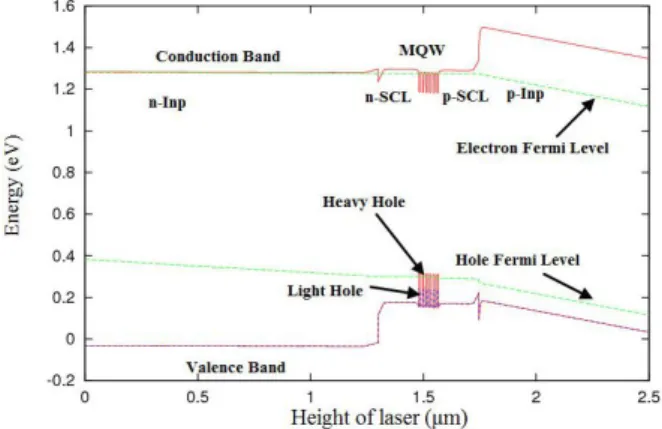
ESULTSThe corresponding band diagram near the laser axis at 30 mA (T=80℃) is illustrated in Fig. 2.
Fig. 2. Energy band diagram at 30 mA (T=80℃). Applying the MQW structure in the active region of the laser was accompanied by the improved performances of the laser parameters such as threshold current, temperature characteristics, and modulation frequency. As
a result, MQW became an essential technology for realizing high-performance lasers. When an MQW system is pumped, the carriers travel in the barriers and drop in the quantum wells. The excess carriers separate the Fermi level into two quasi-Fermi levels. The separation between two quasi-Fermi levels depends on the pump strength. When the pump is strong enough to a separation equal to the material bandgap, the material becomes transparent for photon energies equal to the bandgap. Optical gain is achieved when the system is pumped beyond transparency condition [8].
The laser mode spectrum shown in Fig. 3 confirms that the proposed structure operates at 13.255 μm.
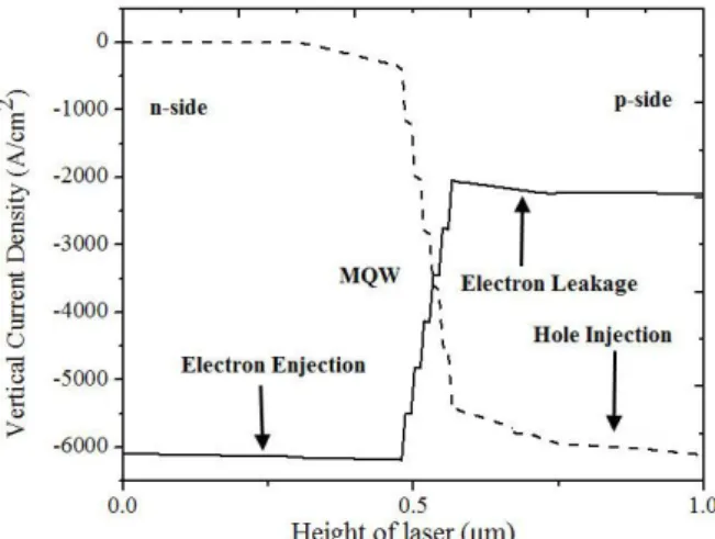
Fig. 3. Laser mode spectrum at 90 mA (T= 80℃). Figure 4 shows the electron and the hole vertical current density profiles in the laser structure.
In Fig. 4, the electron current density in the n-side of the laser and hole current density in the p- side of the structure are shown electron and hole injection, respectively. The presence of electron current density in the p-type layer can be interpreted as the electron leakage current through the MQW region. Figure 4 also indicates that the hole leakage current into the n-type layer is negligible, both because hole motilities are much lower and holes face a larger effective barrier due to their larger effective mass.
Fig. 4. Vertical Current Densities of electrons and holes near the laser axis at an injection current of 90 mA and a stage temperature of 80℃.
The problem of electron leakage current plays an important role in the optical performance of laser diodes, which are mostly operated at high injection levels and high temperatures. Therefore, effects of many factors on leakage current must be considered when designing the active region in a semiconductor laser such as thickness, doping, and strain in the barriers. In the following, the effects of the barrier characterizations on the electron leakage from MQW are investigated.
Fig. 5. Vertical current density of electrons near the laser axis for different p- doping level (solid: no doping, dashed: 2×1017 cm-3, dotted: 2×1018 cm-3) at an injection current of 90 mA and a stage temperature of 80℃.
At the first step, the simulations are repeated with a medium p-doping (2×1017 cm-3) and a high p-doping (2×1018 cm-3) in the barriers.
The vertical current density versus the laser height results is presented in Fig. 5. We observed an increase in the electron leakage current with the increasing barrier doping concentration. Employing p-type doped barriers in the MQW cause electron and hole injection to comparable levels [9]; and thus lowering of barrier heights in the active region due to exchange effect [10]. Low barrier heights lead to the higher escape of carriers outside the active region.
The conduction bands of mentioned structures and bandgap reduction are presented in Fig. 6.
Fig. 6. Conduction Band near the laser axis for different p- doping level (solid: no doping, dashed: 2×1017 cm-3, dotted: 2×1018 cm-3) at an injection current of 90 mA and a stage temperature of 80℃.
Fig. 7. Vertical Current Density of electrons near the laser axis for different barrier thickness at an injection current of 90 mA and a stage temperature of 80℃.
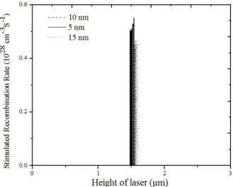
The effect of the barrier width on carrier leakage is another important issue in the design of anMQW laser structure. In the next set of simulations, different thickness barriers are included in the active region. The resulting plots are shown in Fig. 7. It is found theoretically that the device with 5 nm thick barriers is improved in comparison with other structure.
Calculations show that reducing the barrier thickness to a level at which the wells are coupled enhances the hole transport through the barriers and increases recombination with injected electrons. As a result, an increase occurs in stimulated recombination rate. Figure 8 compares stimulated recombination rate in three structures. It is quite obvious that by decreasing barrier thicknesses, the stimulated recombination rate increases. Therefore, fewer electrons will be able to escape the active region and the electron leakage at high current levels decrease and the quantum efficiency improves [11].
Fig. 8. Stimulated Recombination Rate near the laser axis for different barrier thickness at an injection current of 90 mA and a stage temperature of 80℃.
In experimental studies, it is concluded that MQW electric field decrease with decreasing the barrier thickness [12]. A lower electric field results in a better overlap of electron and hole wave functions and better carrier confinement in the quantum wells.
Improvements overlap of carrier wave functions and confinement increase the transition matrix elements, according to the related formula [5], which leads to an increase in stimulated recombination rate. Hence, our simulation results agree with experience. Further improvement of laser performance was expected by introducing a strain in the barriers. In general, the lattice constant of well and barrier must match to that of the substrate to maintain high crystal quality. However, in the MQW structure, the strain caused by lattice mismatch can be accumulated in the crystal by deforming the lattice without generating misfit dislocation since the layer is very thin. By introducing a strain-compensated barrier into the laser, it is possible to grow highly strained quantum wells free of misfit dislocations. In strain-compensated QWs, opposite strains are introduced in the well and barrier regions. These opposite strains balance each other and lead to a decrease in the average strain in the structure. In addition, for some laser configurations, such as short cavity lasers or distributed Bragg reflector lasers, a large number of QWs may be required for optimal performance [13]. As the number of strained QWs is increased, the total strain in the structure accumulates and the total strained layer thickness approaches a critical thickness at which lattice misfit dislocations start to form [14]. In strain-compensated QWs, the well width and the total number of wells can thus be increased, leading to an enhanced optical confinement. By means of introducing strains of opposite signs in the well and barrier layers to simultaneously vary the offsets of the heavy- and light-hole states, it is also possible to reduce the mixing between heavy- and light-hole states by means of spatially separating them to different layers [15]. Experimental results [16, 17] showed that the strain-compensated QW lasers are desirable for optical applications with low threshold current and high efficiency. Therefore, there has been an interest in strain-compensated quantum well structures. Strain compensation gives access to a wider range of material composition and thus improved possibilities to select band edge
offsets tailored to specific device needs [18]. After studying different experimental research, we found that using a barrier with 0.3% tensile strain is conventional in 1300 nm InGaAsP lasers [2, 19].At this stage, the well composition is kept fixed and the barrier bandgap is varied by changing the arsenide mole fraction keeping its strain almost fixed to 0.30% tensile strain. The barrier width must be considered narrow (5 nm) in order to maintain the laser emission around 1325 nm wavelength. Figs. 9 and 10 present the calculated band structures for MQW with unstrained barrier and 0.36% tensile strain, respectively. For both structures, there are four valence bands originating from one light and three heavy hole bands states at k=0.
Fig. 9. In-plane energy dispersion for valence sub-bands in the laser with unstrained barriers.
According to Fig. 10, tensile strain in the barrier causes heavy holes square well to shift such that the separation energy between the HH1 and HH2 bands at k=0 increases compared to the unstrained barrier shown in Fig. 8. As a result, the crossing of the heavy hole bands moves toward higher values of k. Consequently, the highest valence band HH1 maintains its small curvature over a larger range of k. A consequence of the changes in the band structure due to strain is a reduction in the carrier density at transparency. Increasing a band curvature (or equivalently for a parabolic band, reducing its effective mass) makes it easier to populate the state around the band extremum.
Fig. 10. In-plane energy dispersion for valence sub-bands in the laser with tensile strain barriers.
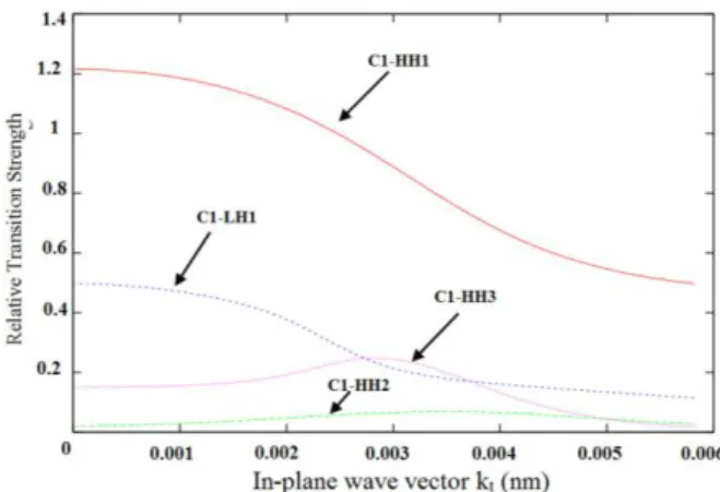
Relative transition strengths for laser with un-strained and 0.36% tensile barrier as a function of the in-plane wave vector kt are plotted in
Figs. 11 and 12, respectively.
Fig. 11. Relative Transition Strength in the laser with unstrained barriers.
Fig. 12. Relative Transition Strength in the laser with tensile strained barriers.
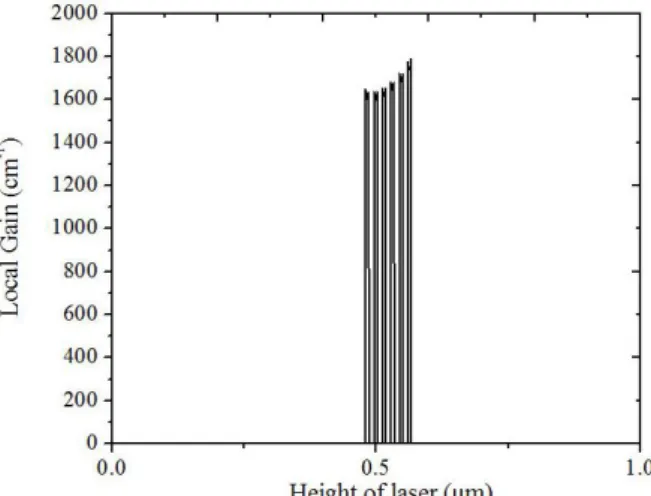
Both MQWs support one quantum level in the conduction band (C1). Allowed transitions are plotted as solid lines; forbidden transitions as dashed lines. As seen in these figures, first heavy-hole transitions are favored under the laser operation. C1–HH1 has the greatest strength; therefore it is the dominant transition. Local gains of different laser structures are compared in Figs. 13 and 14.
Fig. 13. Local Gain near the laser axis for the original structure at an injection current of 90 mA and a stage temperature of 80℃.
Fig. 14. Local Gain near the laser axis for different barrier layer at an injection current of 90 mA and a stage temperature of 80℃.
Comparison of Figs. 13 and 14 shows that using tensile strain in barriers causes to increase gain significantly, leading to an improvement in device performance. In
comparison, the intense non-uniform MQW gain is seen in Fig. 14.
The reasons for this behavior can be understood from the following figures. MQW electron density with and without the barrier tensile strain is represented in Figs. 15 and 16, respectively. Through applying tensile strain in the barriers, the electron concentration increases in the laser active region and leads to an increase in the laser gain. The non-uniformity of electron distribution also occurs in strain compensated MQW.
Fig. 15. Electron Density near the laser axis for the original structure at an injection current of 90 mA and a stage temperature of 80℃.
Fig. 16. Electron Density near the laser axis for different barrier layer at an injection current of 90 mA and a stage temperature of 80℃.
Figure 16 illustrates that the higher the barrier bandgap the more non-uniform is the distribution of the carriers due to the larger energy barrier for thermionic emission between the quantum wells.
Increasing the non-uniformity of the quantum well electron population can be seen in the last barrier near the p-doped side. With such an increase in the population, the electron overflow into p-SCL increases. Therefore, the electron leakage current from MQW must be increased. Fig. 17 confirms this idea.
Fig. 17. Vertical Current Density of electrons near the laser axis for different barrier layer at an injection current of 90 mA and a stage temperature of 80℃.
As shown in Fig. 17, the electron leakage current increases with higher barrier bandgap due to the more non-uniform MQW carrier distribution.
Another important characteristic of the device that changes with the strain is transition energy between the conduction and valance sub-bands and consequently the laser wavelength. The mode spectrum of the laser with tensile strain barriers is shown in Fig. 18. Considering this figure shows that the presence of strain in the barriers leads to some changes in the transition energy; and thus changing the laser wavelength. On the other hand, it should be considered that in the final stage of simulation, the barrier thickness has also decreased, which affects the laser wavelength. As can be seen,
using tensile strain barrier leads to decrease the laser wavelength.
Fig. 18. Laser mode spectrum with tensile barrier at 90 mA (T=80°C).
V.
C
ONCLUSIONIn this work, a typical laser structure for operating at 1.3255 μm was proposed using simulation PICS3D software. Simulation results show that the device suffered from electron leakage. The barrier characterizations affected the leakage current significantly. Increasing doping and reducing barrier thickness leads to increased leakage current. Employing strain caused to increase the gain of the laser but electron non-uniformity occurred. The electron non-uniformity led to increasing the electron leakage current. Using strain in the barrier along with their change in thickness caused to change in the output wavelength.
A
CKNOWLEDGMENTWe express our sincere appreciation to the managers of Cross Light Inc. for providing us with the advanced three-dimensional PICS3D simulation program (version 2008.12) and their kind support.
R
EFERENCES[1] C.H. Henry, The origin of quantum wells and quantum well lasers, In: Zory PS Ed Quantum Well Lasers, New York: Academic Press, 1993.
[2] S. Mogg, Long-Wavelength Vertical-Cavity Lasers: Materials and Device Analysis, Doctoral Dissertation, Royal Institute of Technology, Stockholm, pp. 16–18, 2003.
[3] M. Nadeem Akram, Photonic Devices with MQW Active Material and Waveguide Gratings: Modeling and Characterization, Doctoral Dissertation, Royal Institute of Technology, Stockholm, pp. 25–30, 2005.
[4] F. Hosseinpour and H. Hajihosseini,
“Importance of Simulation in
Manufacturing,” International Journal of Social, Behavioral, Educational, Economic, Business and Industrial Eng. Vol. 3, No. 3, pp. 229–232, 2009.
[5] J. Piprek, Semiconductor optoelectronic devices, Elsevier Science, San Diego, 2003.
[6] I. Vurgaftman and J.R. Meyer, “Band
parameters for ΙΙΙ-V compound
semiconductors and their alloy,” J. Appl. Phys. Vol. 89, pp. 5815–5875, 2001.
[7] Y.K. Kuo, S.H. Yen, M.W. Yao, M.L. Chen, and B.T. Liou, “Numerical study on gain and optical properties of AlGaInAs, InGaNAs, and InGaAsP material systems for 1.3μm semiconductor lasers,” Opt. Commun. Vol. 275, No. 1, pp. 156–164, 2007.
[8] V. Bahrami Yekta and H. Kaatuzian, “Simulationand Temperature Characteristics Improvement of 1.3μm AlGaInAs Multiple Quantum Well Laser,” Int. J. Opt. and Appl. Vol. 4, No. 2, pp. 46–53, 2014.
[9] J. Xie, X. Ni, Q. Fan, R. Shimada, Ü. Özgür, and H. Morkoç, “On the efficiency droop in InGaN multiple quantum well blue light emitting diodes and its reduction with p-doped quantum well barriers,” Appl. Phys. Lett. Vol.93, pp.121107 (1-3), 2008.
[10]Z. Danesh Kaftroudi and E. Rajaei, “Thermal simulation of InP - based 1.3 µm vertical cavity surface emitting laser with AsSb–based DBRs,” Opt. Commun. Vol. 284, pp. 330– 340, 2011.
[11]J. Xie, X. Ni, Q. Fan, R. Shimada, Ü. Özgür, and H. Morkoç, “Reduction of efficiency droop in InGaN light emitting diodes by coupled quantum wells,” Appl. Phys. Lett. Vol. 93, pp. 171113 (1-3), 2008.
[12]G.B. Lin, D.Y. Kim, Q. Shan, J. Cho, E.F. Schubert, H. Shim, C. Sone, and J.K. Kim, “Effect of Quantum Barrier Thickness in the Multiple-Quantum-Well Active Region of GaInN/GaN Light-Emitting Diodes,” IEEE Photon. J. Vol. 5, No. 4, pp. 1600207 (1-7), 2013.
[13]B.I. Miller, U. Koren, M.G. Young, and M. D. Chien, “Strain‐compensated strained‐layer superlattices for 1.5 μm wavelength lasers,” Appl. Phys. Lett. Vol. 58, pp. 1952–1954, 1991.
[14]J.A. Subramaniam, “Critical thickness of
equilibrium epitaxial thin films using finite element method,” J. Appl. Phys. Vol. 95, No. 12, pp. 8472–8474, 2004.
[15]T.E. Whall, A.D. Plews, N.L. Mattey and P.J. Phillips, “Effective mass and band non-parabolicity in remote doped Si/Si0.8Ge0.2
quantum wells,” Appl. Phys. Lett. Vol. 66, No. 20, pp. 2724–2726, 1995.
[16]H. Hwan Park, W. Jeong, and B. Choe, “Strain ‐compensated InGaAs/InGaAsP quantum well lasers lattice matched to GaAs,” Appl. Phys. Lett. Vol. 66, No. 2, pp. 201–203, 1995.
[17]N. Nuntawong, S. Birudavolu, C.P. Hains, S. Huang, H. Xu, and D.L. Huffaker, “Effect of strain-compensation in stacked 1.3µm InAs/GaAs quantum dot active regions grown by metalorganic chemical vapor deposition,” Appl. Phys. Lett. Vol. 85, No. 15, pp. 3050– 3052, 2004.
[18]B. Gonul, F. Kocak, H. Toktam and M. Oduncuoglu, “Theoretical Comparison of the
Band Alignment of Conventionally Strained and Strain-Compensated Phosphorus- Aluminum- and Nitrogen-Based 1.3 μm QW Lasers,” Chin. J. Phys. Vol. 42, No. 6, pp. 764–775, 2004.
[19]Y.W. Mao, Y. Wang, Y.H. Chen, Z.Q. Xue, Q. Lin, Y.M. Duan, and H. Su, “Characteristic Optimization of 1.3 μm High-Speed MQW InGaAsP-AlGaInAs Lasers,”
Chin. Phys. Lett. Vol. 29, No. 6, pp. 064204 (1-4), 2012.
Zahra Danesh Kaftrouddi is an Associate Professor of Physics in the Department of Engineering Sciences of University of Guilan. She received her B.Sc. degree from the Iran University of Science and Technology in 1998 and M.Sc. and Ph.D. degrees from University of Guilan in 2003 and 2010, respectively.
She has academic skills in optoelectronic device simulation.
Abolfazl Mazandarani received his B.Sc. degree in physics from the University of Guilan in 2013. He received his M.Sc. degree from Amirkabir University of Technology in 2015. His research interest is mainly in the laser simulation.