1
3471fbTYPICAL APPLICATION
DESCRIPTION
Dual 1.3A, 1.2MHz
Boost/Inverter in
3mm × 3mm DFN
FEATURES
APPLICATIONS
n 1.2MHz Switching Frequencyn Low VCESAT Switches: 330mV at 1.3A n High Output Voltage: Up to 40V n Wide Input Range: 2.4V to 16V n Inverting Capability
n 5V at 630mA from 3.3V Input n 12V at 320mA from 5V Input n –12V at 200mA from 5V Input
n Uses Tiny Surface Mount Components n Low Shutdown Current: < 1μA
n Low Profi le (0.75mm) 10-Lead 3mm × 3mm
DFN Package
n Organic LED Power Supply n Digital Cameras
n White LED Power Supply n Cellular Phones
n Medical Diagnostic Equipment n Local ±5V or ±12V Supply n TFT-LCD Bias Supply n xDSL Power Supply
The LT®3471 dual switching regulator combines two 42V,
1.3A switches with error amplifi ers that can sense to ground providing boost and inverting capability. The low VCESAT bipolar switches enable the device to deliver high current outputs in a small footprint. The LT3471 switches at 1.2MHz, allowing the use of tiny, low cost and low profi le inductors and capacitors. High inrush current at start-up is eliminated using the programmable soft-start function, where an external RC sets the current ramp rate. A constant frequency current mode PWM architecture results in low, predictable output noise that is easy to fi lter.
The LT3471 switches are rated at 42V, making the device ideal for boost converters up to ±40V as well as SEPIC and fl yback designs. Each channel can generate 5V at up to 630mA from a 3.3V supply, or 5V at 510mA from four alkaline cells in a SEPIC design. The device can be confi gured as two boosts, a boost and inverter or two inverters.
The LT3471 is available in a low profi le (0.75mm) 10-lead 3mm × 3mm DFN package. 4.7k CONTROL 1 3471 TA01 0.33μF 10μF 4.7k CONTROL 2 0.33μF VIN SHDN/SS1 FB1N SW1 SW2 LT3471 10μH 15μH GND FB1P VIN 3.3V FB2P FB2N VREF 0.1μF 4.7μF VOUT1 7V 350mA VOUT2 –7V 250mA 75pF 15k 90.9k 15k 105k 1μF SHDN/SS2 VIN VIN 10μF 2.2μH IOUT (mA) 0 EFFICIENCY (%) 75 80 85 400 3471 TA01b 70 65 50 100 200 300 60 55 95 90 V OUT1 = 7V VOUT1 = –7V
OLED Driver Effi ciency OLED Driver
L, LT, LTC and LTM are registered trademarks of Linear Technology Corporation. All other trademarks are the property of their respective owners.
2
3471fb
PIN CONFIGURATION
ABSOLUTE MAXIMUM RATINGS
(Note 1) VIN Voltage ...16V SW1, SW2 Voltage ... –0.4V to 42V FB1N, FB1P, FB2N, FB2P Voltage... 12V or VIN – 1.5V SHDN/SS1, SHDN/SS2 Voltage ... 16V VREF Voltage ...1.5V Maximum Junction Temperature ... 125°C Operating Temperature Range (Note 2) ...– 40°C to 85°C Storage Temperature Range ...– 65°C to 125°CELECTRICAL CHARACTERISTICS
PARAMETER CONDITIONS MIN TYP MAX UNITS
Minimum Operating Voltage 2.1 2.4 V
Reference Voltage l 0.9910.987 1.000 1.009 1.013 V V Reference Voltage Current Limit (Note 3) 1 1.4 mA Reference Voltage Load Regulation 0mA ≤ IREF ≤ 100μA (Note 3) 0.1 0.2 %/100μA
Reference Voltage Line Regulation 2.6V ≤ VIN ≤ 16V 0.03 0.08 %/V
Error Amplifi er Offset Transition from Not Switching to Switching, VFBP = VFBN = 1V ±2 ±3 mV
FB Pin Bias Current VFB = 1V (Note 3) l 60 100 nA
Quiescent Current VSHDN = 1.8V, Not Switching 2.5 4 mA Quiescent Current in Shutdown VSHDN = 0.3V, VIN = 3V 0.01 1 μA
Switching Frequency 1 1.2 1.4 MHz
Maximum Duty Cycle
l 9086
94 %
%
Minimum Duty Cycle 15 %
Switch Current Limit At Minimum Duty Cycle At Maximum Duty Cycle (Note 4)
1.5 0.9 2.05 1.45 2.6 2.0 A A Switch VCESAT ISW = 0.5A (Note 5) 150 250 mV
Switch Leakage Current VSW = 5V 0.01 1 μA
SHDN/SS Input Voltage High 1.8 V
The ● denotes specifi cations which apply over the full operating
temperature range, otherwise specifi cations are TA = 25°C. VIN = VSHDN = 3V unless otherwise noted.
TOP VIEW 11 DD PACKAGE 10-LEAD (3mm × 3mm) PLASTIC DFN 10 9 6 7 8 4 5 3 2 1 SW1 SHDN/SS1 VIN SHDN/SS2 SW2 FB1N FB1P VREF FB2P FB2N TJMAX = 125°C, θJA = 43°C/ W, θJC = 3°C/W
EXPOSED PAD (PIN 11) IS GND MUST BE SOLDERED TO PCB
ORDER INFORMATION
LEAD FREE FINISH TAPE AND REEL PART MARKING PACKAGE DESCRIPTION TEMPERATURE RANGE
LT3471EDD#PBF LT3471EDD#TRPBF LBHM 10-Lead (3mm × 3mm) Plastic DFN –40°C to 85°C
LEAD BASED FINISH TAPE AND REEL PART MARKING PACKAGE DESCRIPTION TEMPERATURE RANGE
LT3471EDD LT3471EDD#TR LBHM 10-Lead (3mm × 3mm) Plastic DFN –40°C to 85°C Consult LTC Marketing for parts specifi ed with wider operating temperature ranges.
For more information on lead free part marking, go to: http://www.linear.com/leadfree/
3
3471fb
ELECTRICAL CHARACTERISTICS
Quiescent Current
vs Temperature VREF Voltage vs Temperature VREF Voltage vs VREF Current
PARAMETER CONDITIONS MIN TYP MAX UNITS
SHDN Input Voltage Low Quiescent Current ≤ 1μA 0.3 V
SHDN Pin Bias Current VSHDN = 3V, VIN = 4V
VSHDN = 0V 22 0 36 0.1 μA μA
The ● denotes specifi cations which apply over the full operating
temperature range, otherwise specifi cations are TA = 25°C. VIN = VSHDN = 3V unless otherwise noted.
Note 1: Stresses beyond those listed under Absolute Maximum Ratings may cause permanent damage to the device. Exposure to any Absolute Maximum Rating condition for extended periods may affect device reliability and lifetime.
Note 2: The LT3471E is guaranteed to meet performance specifi cations from 0°C to 70°C. Specifi cations over the –40°C to 85°C operating
temperature range are assured by design, characterization and correlation with statistical process controls.
Note 3: Current fl ows out of the pin.
Note 4: See Typical Performance Characteristics for guaranteed current limit vs duty cycle.
Note 5: VCESAT is 100% tested at wafer level only.
TYPICAL PERFORMANCE CHARACTERISTICS
TEMPERATURE (°C) –50 –25
1.6
QUIESCENT CURRENT (mA)
2.0 2.6 0 50 75 3471 G01 1.8 2.4 2.2 25 100 125 TEMPERATURE (°C) –50 –25 0.990 VREF (V) 1.000 1.010 0 50 75 3471 G02 0.995 1.005 25 100 125
VREF CURRENT 200μA/DIV 3471 G03
VREF
VOLTAGE 100mV/DIV
SHDN/SS Current
vs SHDN/SS Voltage Current Limit vs Duty Cycle
Switch Saturation Voltage vs Switch Current SHDN/SS VOLTAGE 1V/DIV 3471 G04 SHDN/SS CURRENT 20μV/DIV VIN = 3.3V VIN > VSHDN/SS DUTY CYCLE (%) 0
CURRENT LIMIT (A)
1.2 1.6 2.2 2.0 80 3471 G05 0.8 0.4 1.0 1.4 1.8 0.6 0.2 0 20 40 60 100 TYPICAL GUARANTEED TA = 25°C SW CURRENT (A) 0 VCESAT (mV) 800 700 600 500 400 300 200 100 0 1.6 3471 G06 0.4 0.8 1.2 1.4 2.0 0.2 0.6 1.0 1.8 90°C 25°C
4
3471fb
FB1N (Pin 1): Negative Feedback Pin for Switcher 1. Connect resistive divider tap here. Minimize trace area at FB1N. Set VOUT = VFB1P(1 + R1/R2), or connect to ground for inverting topologies.
FB1P (Pin 2): Positive Feedback Pin for Switcher 1. Connect either to VREF or a divided down version of VREF, or connect to a resistive divider tap for inverting topologies.
VREF (Pin 3): 1.00V Reference Pin. Can supply up to 1mA of current. Do not pull this pin high. Must be locally bypassed with no less than 0.01μF and no more than 1μF. A 0.1μF ceramic capacitor is recommended. Use this pin as the positive feedback reference or connect a resistor divider here for a smaller reference voltage.
FB2P (Pin 4): Same as FB1P but for Switcher 2.
FB2N (Pin 5): Same as FB1N but for Switcher 2.
SW2 (Pin 6): Switch Pin for Switcher 2 (Collector of in-ternal NPN power switch). Connect inductor/diode here
and minimize the metal trace area connected to this pin to minimize EMI.
SHDN/SS2 (Pin 7): Shutdown and Soft-Start Pin. Tie to 1.8V or more to enable device. Ground to shut down. Soft-start function is provided when the voltage at this pin is ramped slowly to 1.8V with an external RC circuit.
VIN (Pin 8): Input Supply. Must be locally bypassed.
SHDN/SS1 (Pin 9): Same as SHDN/SS2 but for Switcher 1. Note: taking either SHDN/SS pin high will enable the part. Each switcher is individually enabled with its respective
SHDN/SS pin.
SW1 (Pin 10): Same as SW2 but for Switcher 1.
Exposed Pad (Pin 11): Ground. Connect directly to local ground plane. This ground plane also serves as a heat sink for optimal thermal performance.
TYPICAL PERFORMANCE CHARACTERISTICS
Oscillator Frequencyvs Temperature
Peak Switch Current
vs SHDN/SS Voltage Start-Up Waveform (Figure 2 Circuit) TEMPERATURE (°C) –50 1.00 FREQUENCY (MHz) 1.05 1.15 1.20 1.25 1.50 1.35 0 50 75 3471 G07 1.10 1.40 1.45 1.30 –25 25 100 125 VSHDN/SS (V) 0
SWITCH CURRENT (A)
1.2 1.6 2.0 1.6 3471 G08 0.8 0.4 1.0 1.4 1.8 0.6 0.2 0 0.4 0.2 0.6 0.8 1 1.2 1.4 1.8 2.0 TA = 25°C 0.5ms/DIV 3471 G09 ISUPPLY 1A/DIV VOUT1 2V/DIV VOUT2 5V/DIV CONTROL 1 AND 2 5V/DIV
PIN FUNCTIONS
5
3471fb
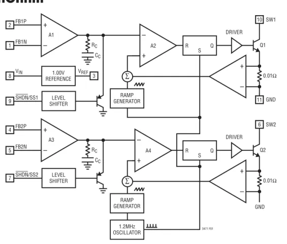
BLOCK DIAGRAM
Figure 1. Block Diagram
OPERATION
The LT3471 uses a constant frequency, current mode control scheme to provide excellent line and load regu-lation. Refer to the Block Diagram. At the start of each oscillator cycle, the SR latch is set, which turns on the power switch, Q1 (Q2). A voltage proportional to the switch current is added to a stabilizing ramp and the resulting sum is fed into the positive terminal of the PWM compara-tor A2 (A4). When this voltage exceeds the level at the negative input of A2 (A4), the SR latch is reset, turning off the power switch Q1 (Q2). The level at the negative input of A2 (A4) is set by the error amplifi er A1 (A3) and is simply an amplifi ed version of the difference between the negative feedback voltage and the positive feedback voltage, usually tied to the reference voltage VREG. In this manner, the error amplifi er sets the correct peak current level to keep the output in regulation. If the error amplifi er’s output increases, more current is delivered to
the output. Similarly, if the error decreases, less current is delivered. Each switcher functions independently but they share the same oscillator and thus the switchers are always in phase. Enabling the part is done by taking either
SHDN/SS pin above 1.8V. Disabling the part is done by grounding both SHDN/SS pins. The soft-start feature of the LT3471 allows for clean start-up conditions by limiting the amount of voltage rise at the output of comparator A1 and A2, which in turn limits the peak switching current. The soft-start feature for each switcher is enabled by slowly ramping that switcher’s SHDN/SS pin, using an RC network, for example. Typical resistor and capacitor values are 0.33μF and 4.7k, allowing for a start-up time on the order of milliseconds. The LT3471 has a current limit circuit not shown in the Block Diagram. The switch current is constantly monitored and not allowed to exceed the maximum switch current (typically 1.6A). If the switch
– + – + R S Q 0.01Ω SW1 DRIVER 10 FB1N SHDN/SS1 1 9 FB1P 2 – + ∑ RAMP GENERATOR 1.00V REFERENCE LEVEL SHIFTER RC CC 1.2MHz OSCILLATOR GND GND Q1 A2 A1 VIN VREF 8 3 – + – + R S Q 0.01Ω SW2 DRIVER 6 11 FB2N SHDN/SS2 5 7 FB2P 4 – + ∑ RAMP GENERATOR LEVEL SHIFTER RC CC 3471 F01 Q2 A4 A3
6
3471fb
OPERATION
APPLICATIONS INFORMATION
Duty Cycle
The typical maximum duty cycle of the LT3471 is 94%. The duty cycle for a given application is given by:
DC= | VOUT|+| VD| –| VIN|
| VOUT|+| VD| –| VCESAT|
Where VD is the diode forward voltage drop and VCESAT is in the worst case 330mV (at 1.3A)
The LT3471 can be used at higher duty cycles, but it must be operated in the discontinuous conduction mode so that the actual duty cycle is reduced.
Setting Output Voltage
Setting the output voltage depends on the topology used. For normal noninverting boost regulator topologies:
VOUT =VFBP 1+R1 R2
where VFBN is connected between R1 and R2 (see the Typical Applications section for examples).
Select values of R1 and R2 according to the following equation: R1=R2 VOUT VREF – 1
A good value for R2 is 15k which sets the current in the resistor divider chain to 1.00V/15k = 67μA.
VFBP is usually just tied to VREF = 1.00V, but VFBP can also be tied to a divided down version of VREF or some other voltage as long as the absolute maximum ratings for the feedback pins are not exceeded (see Absolute Maximum Ratings).
For inverting topologies, VFBN is tied to ground and VFBP is connected between R1 and R2. R2 is between VFBP and VREF and R1 is between VFBP and VOUT (see the Ap-plications section for examples). In this case:
VOUT=VREF R1 R2
Select values of R1 and R2 according to the following equation: R1=R2 VOUT VREF
A good value for R2 is 15k, which sets the current in the resistor divider chain to 1.00V/15k = 67μA.
Switching Frequency and Inductor Selection
The LT3471 switches at 1.2 MHz, allowing for small valued inductors to be used. 4.7μH or 10μH will usually suffi ce. Choose an inductor that can handle at least 1.4A without saturating, and ensure that the inductor has a low DCR (copper-wire resistance) to minimize I2R power losses. Note that in some applications, the current handling requirements of the inductor can be lower, such as in the SEPIC topology where each inductor only carries one half of the total switch current. For better effi ciency, use similar valued inductors with a larger volume. Many different sizes and shapes are available from various manufacturers. Choose a core material that has low losses at 1.2 MHz, such as ferrite core.
Table 1. Inductor Manufacturers
Sumida (847) 956-0666 www.sumida.com TDK (847) 803-6100 www.tdk.com Murata (714) 852-2001 www.murata.com current reaches this value, the SR latch is reset regardless
of the state of the comparator A2 (A4). Also not shown in the Block Diagram is the thermal shutdown circuit. If the temperature of the part exceeds approximately 160°C,
both latches are reset regardless of the state of compara-tors A2 and A4. The current limit and thermal shutdown circuits protect the power switch as well as the external components connected to the LT3471.
7
3471fb
APPLICATIONS INFORMATION
Soft-Start and Shutdown Features
To shut down the part, ground both SHDN/SS pins. To shut down one switcher but not the other one, ground that switcher’s SHDN/SS pin. The soft-start feature provides a way to limit the inrush current drawn from the supply upon start-up. To use the soft-start feature for either switcher, slowly ramp up that switcher’s SHDN/SS pin. The rate of voltage rise at the output of the switcher’s comparator (A1 or A3 for switcher 1 or switcher 2 respectively) tracks the rate of voltage rise at the SHDN/SS pin once the SHDN/SS pin has reached about 1.1V. The soft-start function will go away once the voltage at the SHDN/SS pin exceeds 1.8V. See the Peak Switch Current vs SHDN/SS Voltage graph in the Typical Performance Characteristics section. The rate of voltage rise at the SHDN/SS pin can easily be controlled with a simple RC network connected between the control signal and the SHDN/SS pin. Typical values for the RC network are 4.7kΩ and 0.33μF, giving start-up times on the order of milliseconds. This RC time constant can be adjusted to give different start-up times. If differ-ent values of resistance are to be used, keep in mind the
SHDN/SS Current vs SHDN/SS voltage graph along with the Peak Switch Current vs SHDN/SS Voltage graph, both found in the Typical Performance Characteristics section. The impedance looking into the SHDN/SS pin depends on whether the SHDN/SS is above or below VIN. Normally
SHDN/SS will not be driven above VIN, and thus the imped-ance looks like 100kΩ in series with a diode. If the voltage of the SHDN/SS pin is above VIN, the impedance looks more like 50kΩ in series with a diode. This 100kΩ or 50kΩ impedance can have a slight effect on the start-up time if you choose the R in the RC soft-start network too large. Another consideration is selecting the soft-start time so that the soft-start feature is dominated by the RC network and not the capacitor on VREF. (See VREF voltage reference section of the Applications Information for details.) The soft-start feature is of particular importance in ap-plications where the switch will see voltage levels of 30V or higher. In these applications, the simultaneous presence of high current and voltage during startup may cause an overstress condition to the switch. Therefore, depending on input and output voltage conditions, higher RC time constant values may be necessary to improve the rug-gedness of the design.
CAPACITOR SELECTION
Low ESR (equivalent series resistance) capacitors should be used at the output to minimize the output ripple voltage. Multi-layer ceramic capacitors are an excellent choice, as they have extremely low ESR and are available in very small packages. X5R dielectrics are preferred, followed by X7R, as these materials retain the capacitance over wide voltage and temperature ranges. A 4.7μF to 15μF output capacitor is suffi cient for most applications, but systems with very low output currents may need only a 1μF or 2.2μF output capacitor. Solid tantalum or OS-CON capacitors can be used, but they will occupy more board area than a ceramic and will have a higher ESR. Always use a capacitor with a suffi cient voltage rating.
Ceramic capacitors also make a good choice for the input decoupling capacitor, which should be placed as close as possible to the LT3471. A 4.7μF to 10μF input capacitor is suffi cient for most applications. Table 2 shows a list of several ceramic capacitor manufacturers. Consult the manufacturers for detailed information on their entire selection of ceramic parts.
Table 2. Ceramic Capacitor Manufacturers
Taiyo Yuden (408) 573-4150 www.t-yuden.com AVX (803) 448-9411 www.avxcorp.com Murata (714) 852-2001 www.murata.com The decision to use either low ESR (ceramic) capacitors or the higher ESR (tantalum or OS-CON) capacitors can affect the stability of the overall system. The ESR of any capacitor, along with the capacitance itself, contributes a zero to the system. For the tantalum and OS-CON ca-pacitors, this zero is located at a lower frequency due to the higher value of the ESR, while the zero of a ceramic capacitor is at a much higher frequency and can generally be ignored.
A phase lead zero can be intentionally introduced by placing a capacitor (CPL) in parallel with the resistor (R3) between VOUT and VFB as shown in Figure 2. The frequency of the zero is determined by the following equation.
ƒZ= 1
8
3471fb
APPLICATIONS INFORMATION
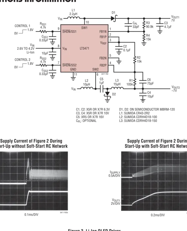
Supply Current of Figure 2 During Start-Up without Soft-Start RC Network
Supply Current of Figure 2 During Start-Up with Soft-Start RC Network
RSS1 4.7k RSS2 4.7k CONTROL 1 3471 F02 CSS1 0.33μF CSS2 0.33μF 10μF VIN 2.6V TO 4.2V Li-Ion SHDN/SS1 FB1N 9 0V 1.8V CONTROL 2 0V 1.8V 8 7 SW1 SW2 LT3471 L2 10μH L3 15μH GND FB1P VIN FB2P FB2N VREF C2 0.1μF C3 4.7μF CPL 33pF VOUT1 7V VOUT2 –7V C1, C2: X5R OR X7R 6.3V C3, C4: X5R OR X7R 10V C5: XR5 OR X7R 16V CPL: OPTIONAL D1, D2: ON SEMICONDUCTOR MBRM-120 L1: SUMIDA CR43-2R2 L2: SUMIDA CDRH4D18-100 L3: SUMIDA CDRH4D18-150 C6 75pF R2 15k R3 90.9k R4 15k R1 105k C5 1μF SHDN/SS2 VIN 10 1 2 3 5 4 11 6 VIN C4 10μF D2 L1 2.2μH D1
Figure 2. Li-Ion OLED Driver
0.1ms/DIV 3471 F02b ISUPPLY 0.5A/DIV VOUT1 2V/DIV VIN = 3.3V VIN > VSHDN/SS 0.2ms/DIV 3471 F02c ISUPPLY 0.5A/DIV VOUT1 2V/DIV VIN = 3.3V VIN > VSHDN/SS
9
3471fb
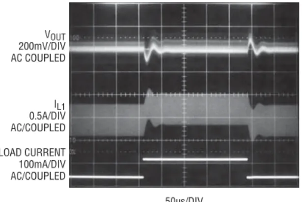
By choosing the appropriate values for the resistor and capacitor, the zero frequency can be designed to improve the phase margin of the overall converter. The typical target value for the zero frequency is between 35kHz to 55kHz. Figure 3 shows the transient response of the step-up converter from Figure 2 without the phase lead capacitor CPL. Although adequate for many applications, phase margin is not ideal as evidenced by 2-3 “bumps” in both the output voltage and inductor current. A 33pF capacitor for CPL results in ideal phase margin, which is revealed in Figure 4 as a more damped response and less overshoot.
Figure 3. Transient Response of Figure 2’s Step-Up Converter without Phase Lead Capacitor
Figure 4. Transient Response of Figure 2’s Step-Up Converter with 33pF Phase Lead Capacitor
VREG VOLTAGE REFERENCE
Pin 3 of the LT3471 is a bandgap voltage reference that has been divided down to 1.00V and buffered for external use. This pin must be bypassed with at least 0.01μF and no more than 1μF. This will ensure stability as well as reduce the noise on this pin. The buffer has a built-in current limit of at least 1mA (typically 1.4mA). This not only means that you can use this pin as an external reference for supplemental circuitry, but it also means that it is possible to provide a soft-start feature if this pin is used as one of the feedback pins for the error amplifi er. Normally the soft-start time will be dominated by the RC time constant discussed in the soft-start and shutdown section. However, because of the fi nite current limit of the buffer for the VREG pin, it will take some time to charge up the bypass capacitor. During this time, the voltage at the VREG pin will ramp up, and this action provides an alternate means for soft-starting the circuit. If the largest recommended bypass capacitor is used, 1μF, the worst-case (longest) soft-start function that would be provided from the VREF pin is:
1μF • 1.00V
1.0mA =1.0ms
Choose the RC network such that the soft-start time is longer than this time, or choose a smaller bypass capacitor for the VREF pin (but always larger than 0.01μF) so that the RC network dominates the soft-starting of the LT3471. The voltage at the VREF pin can also be divided down and used for one of the feedback pins for the error amplifi er. This is especially useful in LED driver applications, where the current through the LEDs is set using the voltage reference across a sense resistor in the LED chain. Using a smaller or divided down reference leads to less wasted power in the sense resistor. See the Typical Applications section for an example of LED driving applications.
APPLICATIONS INFORMATION
50μs/DIV IL1 0.5A/DIV AC/COUPLED LOAD CURRENT 100mA/DIV AC/COUPLED VOUT 200mV/DIV AC COUPLED VIN = 3.3V VIN > VSHDN/SS 50μs/DIV IL1 0.5A/DIV AC/COUPLED LOAD CURRENT 100mA/DIV AC/COUPLED VOUT 200mV/DIV AC COUPLED VIN = 3.3V VIN > VSHDN/SS10
3471fb
APPLICATIONS INFORMATION
DIODE SELECTION
A Schottky diode is recommended for use with the LT3471. For high effi ciency, a diode with good thermal characteristics at high currents should be used such as the On Semiconductor MBRM120. This is a 20V diode. Where the switch voltage exceeds 20V, use the MBRM140, a 40V diode. These diodes are rated to handle an average forward current of 1.0A. In applications where the average forward current of the diode is less than 0.5A, use the Philips PMEG 2005, 3005, or 4005 (a 20V, 30V or 40V diode, respectively).
LAYOUT HINTS
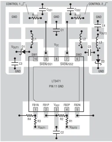
The high speed operation of the LT3471 demands care-ful attention to board layout. You will not get advertised performance with careless layout. Figure 5 shows the recommended component placement.
Compensation—Theory
Like all other current mode switching regulators, the LT3471 needs to be compensated for stable and effi cient operation. Two feedback loops are used in the LT3471: a fast current loop which does not require compensation, and a slower voltage loop which does. Standard Bode plot analysis can be used to understand and adjust the voltage feedback loop.
As with any feedback loop, identifying the gain and phase contribution of the various elements in the loop is critical. Figure 6 shows the key equivalent elements of a boost con-verter. Because of the fast current control loop, the power stage of the IC, inductor and diode have been replaced by the equivalent transconductance amplifi er gmp. gmp acts as a current source where the output current is proportional to the VC voltage. Note that the maximum output current of gmp is fi nite due to the current limit in the IC.
– + – + gma RC RO R2 CC: COMPENSATION CAPACITOR
COUT: OUTPUT CAPACITOR
CPL: PHASE LEAD CAPACITOR
gma: TRANSCONDUCTANCE AMPLIFIER INSIDE IC
gmp: POWER STAGE TRANSCONDUCTANCE AMPLIFIER
RC: COMPENSATION RESISTOR
RL: OUTPUT RESISTANCE DEFINED AS VOUT DIVIDED BY ILOAD(MAX) RO: OUTPUT RESISTANCE OF gma
R1, R2: FEEDBACK RESISTOR DIVIDER NETWORK RESR: OUTPUT CAPACITOR ESR
3471 F06 R1 COUT CPL RESR RL VOUT VC CC gmp 1.00V REFERENCE
Figure 6. Boost Converter Equivalent Model
Figure 5. Suggested Layout Showing a Boost on SW1 and an Inverter on SW2. Note the Separate Ground Returns for All High Current Paths (Using a Multilayer Board)
10 GND GND SHDN/SS1 9 8 7 SHDN/SS2 FB1N R4 R2 R3 FB1P VOUT1 R1 C2 3471 F05 C3 CSS1 CSS2 RSS1 RSS2 C1 • • C4 D2 VOUT1 VOUT2 SW1 SW2 C5 D1 L1 L2 L3 VOUT2 FB2P FB2N VREF 6 1 2 3 4 5 LT3471 PIN 11 GND VCC GND GND GND CONTROL 1 CONTROL 2
11
3471fb
APPLICATIONS INFORMATION
Figure 7. Bode Plot of 3.3V to 7V Application
From Figure 6, the DC gain, poles and zeroes can be calculated as follows:
Output Pole: P1= 2 2 •π•RL• COUT
Error Amp Pole: P2= 1 2 •π•RO• CC Error Amp Zero: Z1= 1
2 •π•RC• CC DC GAIN: A=VREF VOUT • gma•RO• gmp•RL • 1 2 ESR Zero: Z2= 1 2 •π•RESR• COUT RHP Zero: Z3= VIN2•RL 2 •π• VOUT2•L
High Frequency Pole: P3>fS 3 Phase Lead Zero: Z4= 1
2 •π•R1• CPL Phase Lead Pole: P4= 1
2 •π• CPL•R1•R2 R1+R2
The Current Mode zero is a right half plane zero which can be an issue in feedback control design, but is manageable with proper external component selection.
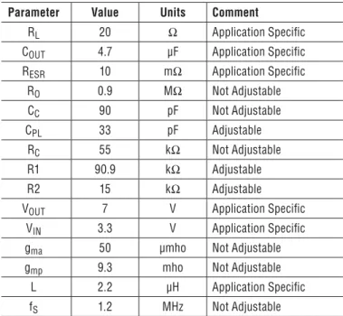
Using the circuit of Figure 2 as an example, Table 3 shows the parameters used to generate the Bode plot shown in Figure 7.
Table 3. Bode Plot Parameters
Parameter Value Units Comment
RL 20 Ω Application Specifi c
COUT 4.7 μF Application Specifi c
RESR 10 mΩ Application Specifi c
RO 0.9 MΩ Not Adjustable CC 90 pF Not Adjustable CPL 33 pF Adjustable RC 55 kΩ Not Adjustable R1 90.9 kΩ Adjustable R2 15 kΩ Adjustable VOUT 7 V Application Specifi c
VIN 3.3 V Application Specifi c
gma 50 μmho Not Adjustable
gmp 9.3 mho Not Adjustable
L 2.2 μH Application Specifi c fS 1.2 MHz Not Adjustable
From Figure 7, the phase is –115° when the gain reaches 0dB giving a phase margin of 65°. This is more than adequate. The crossover frequency is 50kHz.
FREQUENCY (Hz) 0 GAIN (dB) PHASE (DEG) 60 70 –10 –20 50 20 40 30 10 100 10k 100k 1M 3471 F07 –30 –350 –50 0 –100 –250 –150 –200 –300 –400 1k GAIN PHASE
12
3471fbTYPICAL APPLICATIONS
RSS1 4.7k RSS24.7k CONTROL 1 3471 TA02 CSS1 0.33μF CSS2 0.33μF C1 10μF VIN 2.6V TO 4.2V Li-Ion SHDN/SS1 FB1N 9 0V 1.8V CONTROL 2 0V 1.8V 8 7 SW1 SW2 LT3471 L2 15μH L3 15μH GND FB1P VIN FB2P FB2N VREF C2 0.1μF C3 4.7μF C6 33pF VOUT1 7V 500mA WHEN VIN = 4.2V 350mA WHEN VIN = 3.3V 250mA WHEN VIN = 2.6V VOUT2 –7V TO –4V –7V WHEN VCONTROL = 0V –4V WHEN VCONTROL = 1 –7V, 300mA WHEN VIN = 4.2V –7V, 250mA WHEN VIN = 3.3V –7V, 200mA WHEN VIN = 2.6V C1, C2: X5R OR X7R 6.3V C3, C4: X5R OR X7R 10V C5: XR5 OR X7R 16V C6: OPTIONAL D1, D2: ON SEMICONDUCTOR MBRM-120 L1: SUMIDA CR43-2R2 L2: SUMIDA CDRH4D18-100 L3: SUMIDA CDRH4D18-150 C6 75pF R2 15k R5 20k R6 10k R3 90.9k R4 15k R1 105k C5 1μF SHDN/SS2 VIN 10 1 2 3 5 4 11 6 VIN C4 10μF D2 L1 2.2μH D1 VCONTROL 0V TO 1V IOUT (mA) 0 50 EFFICIENCY (%) 55 65 70 75 200 400 500 95 3471 TA02b 60 100 300 80 85 90 VOUT = 7V V IN = 4.2V VIN = 4.2V VIN = 3.3V VIN = 3.3V VIN = 2.6V VIN = 2.6V VOUT = –7VLi-Ion OLED Driver Effi ciency Li-Ion OLED Driver
13
3471fb
TYPICAL APPLICATIONS
Single Li-Ion Cell to 5V, 12V Boost Converter
RSS1 4.7k RSS2 4.7k CONTROL 1 3471 TA03 CSS1 0.33μF CSS2 0.33μF C1 4.7μF VIN 2.6V TO 4.2V SHDN/SS1 FB1N 9 OV 1.8V 1.8V 0V CONTROL 2 8 7 SW1 SW2 LT3471 L2 6.8μH GND FB1P VIN FB2N FB2P VREF C2 0.1μF C3 10μF C5 100pF C6 220pF VOUT1 5V 900mA IF VIN = 4.2V 630mA IF VIN = 3.3V 425mA IF VIN = 2.6V VOUT2 12V 300mA IF VIN = 4.2V 210mA IF VIN = 3.3V 145mA IF VIN = 2.6V C1-C3: X5R OR X7R 6.3V C4: X5R OR X7R 16V D1, D2: ON SEMICONDUCTOR MBRM-120 L1: SUMIDA CR43-3R3 L2: SUMIDA CR43-6R8 R1 20k R2 4.99k R3 54.9k R4 4.99k SHDN/SS2 VIN 10 1 2 3 4 5 11 6 VIN C4 10μF L1 3.3μH D1 D2
14
3471fb
TYPICAL APPLICATIONS
Li-Ion 20 White LED Driver
RSS1 4.7k RSS2 4.7k 3471 TA04 CSS1 0.33μF CSS2 0.33μF C1 4.7μF VIN 2.6V TO 4.2V SHDN/SS1 FB1N 9 8 7 SW1 SW2 LT3471 L2 2.2μH GND FB1P VIN FB2N FB2P VREF C2 0.1μF R1 90.9k C3 0.22μF I20mAOUT1 C1, C2: X5R OR X7R 6.3V C3, C4: X5R OR X7R 50V D1, D2: ON SEMICONDUCTOR MBRM-140 L1, L2: SUMIDA CDRH2D-2R2 R2 10k 4.99Ω SHDN/SS2 VIN 10 1 2 3 4 5 11 6 VIN C4 0.22μF L1 2.2μH D1 D2 IOUT2 20mA 10 WHITE LEDs 10 WHITE LEDs 4.99Ω CONTROL 1 OV 1.8V CONTROL 2 OV 1.8V
15
3471fb
Information furnished by Linear Technology Corporation is believed to be accurate and reliable. However, no responsibility is assumed for its use. Linear Technology Corporation makes no representa-tion that the interconnecrepresenta-tion of its circuits as described herein will not infringe on existing patent rights.
TYPICAL APPLICATIONS
DD Package 10-Lead Plastic DFN (3mm × 3mm) (Reference LTC DWG # 05-08-1698) 3.00±0.10 (4 SIDES) NOTE:1. DRAWING TO BE MADE A JEDEC PACKAGE OUTLINE M0-229 VARIATION OF (WEED-2). CHECK THE LTC WEBSITE DATA SHEET FOR CURRENT STATUS OF VARIATION ASSIGNMENT 2. DRAWING NOT TO SCALE
3. ALL DIMENSIONS ARE IN MILLIMETERS
4. DIMENSIONS OF EXPOSED PAD ON BOTTOM OF PACKAGE DO NOT INCLUDE MOLD FLASH. MOLD FLASH, IF PRESENT, SHALL NOT EXCEED 0.15mm ON ANY SIDE 5. EXPOSED PAD SHALL BE SOLDER PLATED
6. SHADED AREA IS ONLY A REFERENCE FOR PIN 1 LOCATION ON THE TOP AND BOTTOM OF PACKAGE
0.38± 0.10
BOTTOM VIEW—EXPOSED PAD 1.65± 0.10 (2 SIDES) 0.75±0.05 R = 0.115 TYP 2.38±0.10 (2 SIDES) 1 5 10 6 PIN 1 TOP MARK (SEE NOTE 6) 0.200 REF 0.00 – 0.05 (DD) DFN 1103 0.25± 0.05 2.38±0.05 (2 SIDES)
RECOMMENDED SOLDER PAD PITCH AND DIMENSIONS 1.65±0.05 (2 SIDES) 2.15±0.05 0.50 BSC 0.675±0.05 3.50±0.05 PACKAGE OUTLINE 0.25± 0.05 0.50 BSC
Li-Ion or 4-Cell Alkaline to 3.3V and 5V SEPIC
RSS1 4.7k RSS2 4.7k 3471 TA05 CSS1 0.33μF CSS2 0.33μF C1 4.7μF VIN 2.6V TO 6.5V SHDN/SS1 FB1N 9 8 7 SW1 SW2 LT3471 L3 10μH GND FB1P VIN FB2N FB2P VREF C2 0.1μF C4 15μF C7 56pF C8 56pF C3 4.7μF C5 10μF VOUT1 3.3V 640mA AT VIN = 6.5V 550mA AT VIN = 5V 470mA AT VIN = 4V 410mA AT VIN = 3.3V 340mA AT VIN = 2.6V VOUT2 5V 500mA AT VIN = 6.5V 420mA AT VIN = 5V 360mA AT VIN = 4V 300mA AT VIN = 3.3V 250mA AT VIN = 2.6V C1, C3, C5: X5R OR X7R 10V C4, C6: X5R OR X7R 6.3V D1, D2: ON SEMICONDUCTOR MBRM-120 L1-L4: MURATA LQH43CN100K032 R1 34.8k L2 10μH R2 15k R3 60.4k R4 15k SHDN/SS2 VIN 10 1 2 3 4 5 11 6 VIN C6 15μF L1 10μH D1 D2 L4 10μH CONTROL 1 OV 1.8V CONTROL 2 OV 1.8V
PACKAGE DESCRIPTION
16
3471fb
Linear Technology Corporation
1630 McCarthy Blvd., Milpitas, CA 95035-7417
(408) 432-1900 ● FAX: (408) 434-0507 ● www.linear.com © LINEAR TECHNOLOGY CORPORATION 2004
LT 1008 REV B • PRINTED IN USA
TYPICAL APPLICATIONS
RELATED PARTS
PART NUMBER DESCRIPTION COMMENTS
LT1611 550mA (ISW), 1.4MHz, High Effi ciency Micropower Inverting
DC/DC Converter
VIN: 1.1V to 10V, VOUT(MAX) = –34V, IQ = 3mA, ISD < 1μA,
ThinSOT Package LT1613 550mA (ISW), 1.4MHz, High Effi ciency Step-Up
DC/DC Converter
VIN: 0.9V to 10V, VOUT(MAX) = 34V, IQ = 3mA, ISD < 1μA,
ThinSOT Package LT1614 750mA (ISW), 600kHz, High Effi ciency Micropower Inverting
DC/DC Converter
VIN: 1V to 12V, VOUT(MAX) = –24V, IQ = 1mA, ISD < 10μA,
MS8, S8 Packages LT1615/LT1615-1 300mA/80mA (ISW), High Effi ciency Step-Up
DC/DC Converters
VIN = 1V to 15V, VOUT(MAX) = 34V, IQ = 20μA, ISD < 1μA,
ThinSOT Package LT1617/LT1617-1 350mA/100mA (ISW), High Effi ciency Micropower Inverting
DC/DC Converters
VIN = 1.2V to 15V, VOUT(MAX) = –34V, IQ = 20μA, ISD < 1μA,
ThinSOT Package LT1930/LT1930A 1A (ISW), 1.2MHz/2.2MHz, High Effi ciency Step-Up
DC/DC Converters
VIN: 2.6V to 16V, VOUT(MAX) = 34V, IQ = 4.2mA/5.5mA,
ISD < 1μA, ThinSOT Package
LT1931/LT1931A 1A (ISW), 1.2MHz/2.2MHz High Effi ciency Micropower Inverting
DC/DC Converters
VIN = 2.6V to 16V, VOUT(MAX) = –34V, IQ = 5.8mA, ISD < 1μA,
ThinSOT Package LT1943 (Quad) Quad Boost, 2.6A Buck, 2.6A Boost, 0.3A Boost, 0.4A Inverter
1.2MHz TFT DC/DC Converter
VIN = 4.5V to 22V, VOUT(MAX) = 40V, IQ = 10μA, ISD < 35μA,
TSSOP28E Package LT1945 (Dual) Dual Output, Boost/Inverter, 350mA (ISW), Constant Off-Time,
High Effi ciency Step-Up DC/DC Converter
VIN = 1.2V to 15V, VOUT(MAX) = ±34V, IQ = 40μA, ISD < 1μA,
10-Lead MS Package LT1946/LT1946A 1.5A (ISW), 1.2MHz/2.7MHz, High Effi ciency Step-Up
DC/DC Converters
VIN: 2.45V to 16V, VOUT(MAX) = 34V, IQ = 3.2mA, ISD < 1μA,
MS8 Package
LT3436 3A (ISW), 1MHz, 34V Step-Up DC/DC Converter VIN: 3V to 25V, VOUT(MAX) = 34V, IQ = 0.9mA, ISD < 6μA,
TSSOP16E Package LT3462/LT3462A 300mA (ISW), 1.2MHz/2.7MHz, High Effi ciency Inverting
DC/DC Converters with Integrated Schottkys
VIN = 2.5V to 16V, VOUT(MAX) = –38V, IQ = 2.9mA, ISD < 1μA,
ThinSOT Package LT3463/LT3463A Dual Output, Boost/Inverter, 250mA (ISW), Constant Off-Time,
High Effi ciency Step-Up DC/DC Converters with Integrated Schottkys
VIN = 2.3V to 15V, VOUT(MAX) = ±40V, IQ = 40μA, ISD < 1μA,
DFN Package LT3464 85mA (ISW), High Effi ciency Step-Up DC/DC Converter with
Integrated Schottky and PNP Disconnect
VIN = 2.3V to 10V, VOUT(MAX) = 34V, IQ = 25μA, ISD < 1μA,
ThinSOT Package
5V to ±12V Dual Supply Boost/Inverting Converter
4.7k 4.7k 3471 TA06 0.33μF 0.33μF C1 4.7μF VIN 5V SHDN/SS1 FB1N 9 8 7 SW1 SW2 LT3471 L2 10μH C5 1μF GND FB1P VIN FB2N FB2P VREF C2 0.1μF C3 4.7μF C6 56pF VOUT1 12V 320mA VOUT2 –12V 200mA C1, C2: X5R OR X7R 6.3V C3, C4: X5R OR X7R 16V C5: X5R OR X7R 25V D1, D2: ON SEMICONDUCTOR MBRM-120 L1: SUMIDA CR43-10 L2, L3: SUMIDA CLS63-10 R1 54.9k R2 4.99k R3 15k R4 182k SHDN/SS2 VIN 10 1 2 3 4 5 11 6 • VIN C4 4.7μF C7 56pF L1 10μH D1 D2 10μHL3 • CONTROL 1 OV 1.8V CONTROL 2 OV 1.8V