__________________
Corresponding Author. Mail. [email protected]
6
Innovative Research in Engineering Sciences Vol 2(4), 6-11 (2016)
Journal of Innovative research in engineering sciences
Journal homepage :
www.Joires.com
A Novel Micro-Switch Capable of Handling RF Powers Higher than 5W
Abdolreza Gharehkhani1*, Ebrahim Abbaspour-Sani2
1 PhD student, Department of Electrical Engineering, Urmia University, Urmia, Iran. 2 Associated professor, Department of Electrical Engineering, Urmia University, Urmia, Iran.
Abstract: A new structural design employing surface micromachining is proposed for a shunt capacitive switch capable of transferring powers higher than 5 Wat a frequency of 2.4 GHz. The actuation voltage is low enough so that the micro switch resists switching due to the transferring RF power as high as 5W.It also can stand against any unwanted acceleration forces applied to the switch along the Z-axes. The simulated results for the S parameters are:S11 -31.5 dB in up mode and -0.13 dB in down mode; while,S12 equals -0.047 dB in up
mode and -36.2 dB in down mode. The simulated results also indicate that the percentage of the reflected power is lower than 0.1% in up mode and higher than 97.5% in down mode. All the aforementioned is a proof of a very good performance of the designed switch and shows that the designed switch despite its capability of transferring powers higher than 5 W has a low insertion loss and a high isolation.
Key words: Microelectromechanical systems (MEMS), surface Micromachining, Shunt Capacitive Switch, actuation voltage, Insertion loss, Isolation.
1. Introduction
Switch as one of the RF MEMS parts have attracted a lot of studies. The earliest MEMS switch has been made by Peterson in 1979. He used a micro machine cantilever beam as a switch [1]. Later in 1990, the RF MEMS switch for microwave usages was designed [2] and explained in detail by Larson [3]. The idea of combination of the structures of mechanical switches and semiconductor switches, and considering the advantages and disadvantages of each of the aforementioned switches led to advent of microelectromechanical switches. The MEMS switches with both mechanical and semiconductor aspects have capabilities such as proper isolation and loss, small size and desired speed [4]. Study on micro switches is vital because of the wide range of their applications in creating switching networks, digital modulation, phase shifters, wireless communications [5,6], and in other sectors of electronics and telecommunications industries MEMS switches have two different stable positions and alternation between these two positions is done through the movement of a plate or a lever which has a cantilever on one end or on both ends. The switch can operate once a particular amount of force is applied to the movable part of the MEMS switch according to a variety of mechanisms such as electrostatic, electromagnetic, electro-thermal and piezoelectric forces [7,8,9]. This –depending on thickness, length, and material of the movable parts of the switch– will lead to a particular amount of movement of the movable part of the switch and as a result its operation. There are different types of MEMS
switches which can be categorized based on the mechanism, type of contact and incorporation type of switches in circuits (series or parallel) [10]. MEMS switches can be made of plates or levers which have cantilever in one or both ends. The metal contact for ohmic contacts [11], or metal-insulator-metal contact for capacitor contacts can be used to make the switches. In the proposed design Shunt Capacitive Switch is used.
7
2. Structure of the proposed micro switchAs it can be seen in
Error! Reference source not
found.
, in the proposed shunt switch on line of CPW, the green path (a), is the path of RF signal and the main electrostatic force is applied from this section. The blue parts (b), makes the ground, and the movable part of the structure is connected to the ground via two anchors. Moreover, the two red plates (c), were designed to create an extra electrostatic force. This extra electrostatic force along with the main electrostatic force created through RF path, are used to move the upper electrode where results in a higher power transfer ability without unwanted switching. The thickness of the fixed parts of the CPW line and movable arms of the switch are 2μ𝑚 and 2.5μ𝑚 respectively. To show the length and width of different parts of the designed structure, its vertical view is displayed in Figure 2 Considering the scaling of the figure, sizes of the length and width of different parts of the switch are identifiable (Each square equals 50 𝜇𝑚 ∗ 50 𝜇𝑚).Figure 2. Vertical view of the designed switch in form of scaling
It is noticeable that the aforementioned sizes were determined by considering two factors i) appropriate mechanical and electromagnetic performance ii) particular impedance of 50Ω for transference line of CPW [12].
Figure 3. Sizes of CPW line with silicon substructure obtained from the software
Theoretically, the process is as follows: switch is in up mode as long as electrostatic voltage is not applied.
Considering the size of the gap which is 3.9 μ𝑚, capacitance of the capacitor would be:
𝐶1= 𝜀0𝜀𝑟
𝐴
𝑑= 8.85 × 10
−12× 1 × 𝐴
3.9𝜇 (1)
When the arms are lowered, the upper plate contacts the 0.05μ𝑚nitride which is on RF path (𝑆𝑖3𝑁4 has𝜀𝑟= 7 ) and
capacitance of the capacitor changes as follows:
𝐶2= 𝜀0𝜀𝑟
𝐴
𝑑= 8.85 × 10
−12× 7 × 𝐴
0.05𝜇 (2)
𝐶2= 7 ×
3.9𝜇
0.05𝜇𝐶1= 546𝐶1 (3)
In other words, theoretically, capacitance of the capacitor in down mode is 546 times larger than its capacitance in up mode and as a result the amount of impedance decreases drastically.
𝑍𝑢𝑝=
1 𝑗𝑤𝐶1
= 1
𝑗2.4𝐺 × 𝐶1
𝑓𝑜𝑟 𝑢𝑝 𝑠𝑡𝑎𝑡𝑒 (4)
𝑍𝑑𝑜𝑤𝑛=
1 𝑗𝑤𝐶2
= 1
𝑗2.4𝐺 × 546 × 𝐶1
𝑓𝑜𝑟 𝑑𝑜𝑤𝑛 𝑠𝑡𝑎𝑡𝑒 (5)
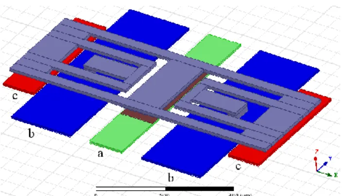
Figure 4. Equivalent circuit of a shunt capacitive switch
Therefore a drastic decrease in impedance will cause a change in signal path [13].
Meanwhile, thickness of the movable plate (2.5 𝜇𝑚) for spring arms is taken a little more in the present study, so that it is not bent at the time of switch performance and consequently the changes in capacitance are more desirable. (Bossed) [14].
3. The switch performance analysis
3.1. Analysis of the mechanical performance
For transference of 5W power through CPW with 𝑍0=
50Ω , the maximum possible voltage which can be applied to the movable part through RF path can be.
𝑉 = √𝑃𝑍0= √5 × 50 = 15.8 (6)
Therefore mechanical design for switch performance is done according to the minimum voltage of 15.8 V. Therefore, the possibility of error of unwanted switching while transferring 5W power is eliminated.
The mechanical behavior of the switch was analyzed using the COMSOL software [13].
8
due to transference of a power higher than 5W); in worst case scenario, the structure can move just 0.85 𝜇𝑚. By considering the 3.9 𝜇𝑚 air gap, with such movement the system cannot reach to the distance of 1/3 gap (pull-in voltage point), where in practice no switching will be occurred. Meanwhile the distance between the upper plate and the lower electrode will still be more than 3μ𝑚 and this itself is promising that 𝑆11 parameter will still be desirable.We will discuss this parameter in the electromagnetic analysis section.
Case 2: Now in another case, dc voltage is applied up to 16V both through RF path and at the same time through the plates of the two sides of the grounds which are taken for applying the extra electrostatic force. Through applying 16V voltage, the upper plate moves about 1.4𝜇𝑚 which is more than 1/3 gap of 3.9μm air gap, so at this point pull-in voltage occurs and the upper plate contacts the lower electrode (on0.05𝜇𝑚 nitride) and as said before capacitance of the capacitor increases drastically and causes drastic decrease in impedance and switching happens. Also results of COMSOL software showed that the maximum stress applied to the structure which is due to the movement of the movable part is 0.01 G Pa which can be acceptable. All the aforementioned results in this section shows proper mechanical performance of the designed switch in transferring 5W power when on and off orders are executed.
Figure 5. The switch displacement versus applied electrostatic force just through RF path
Figure 6. Exaggerated display of the movement path when the electrostatic force is applied both through RF path and through the two plates which are on two sides of the grounds and are there
for creating extra electrostatic force.
Figure 7. The switch displacement, when the electrostatic force is applied both through RF path and through the two plates which
9
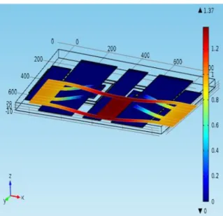
Figure 8. Display of distribution of surface current for the upmode
Figure 9. Display of distribution of surface current for the down mode
3.2. Analysis of electromagnetic performance
In the former section, the proposed design was studied regarding its mechanical behavior. It was mentioned that the maximum voltage which can be applied to the movable part through transference of 5W power through RF path is 15.8 V. According to the mechanical design, the possibility of error of unwanted switching was eliminated.
Using the electromagnetic analysis it is endeavored to see in the proposed design, what voltage can be created between the two upper and lower plates in line with RF path. Using HFSS software, the maximum electrical field of E between the two plates in the up mode is obtained (value of E is4.07 × 106) and using equation (7) the resulting
voltage is calculated.
𝑉 = ∫ 𝐸 . 𝑑𝑧 = 𝐸 × 3.9𝜇 = 4.07 × 10⁶ 𝑔𝑎𝑝
0
× 3.9𝜇
= 15.87 𝑉 (7)
As it is shown in this method the amount of the voltage is obtained 15.87 which is similar to the results obtained using the mechanical performance analysis. It is notable that in analysis of the mechanical structure it was known that this structure was resistant to even unwanted voltages bigger than 16 V. According to the results of the simulations with
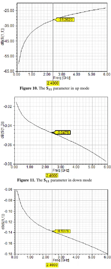
HFSS software, distribution parameters of S for the designed structure in up and down modes are presented in fig.10 to fig.13 and Table 1.
Figure 10. The 𝐒𝟏𝟏 parameter in up mode
Figure 11. The 𝐒𝟏𝟏 parameter in down mode
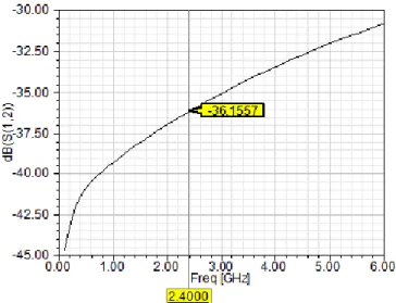
10
Figure 13. The 𝐒𝟏𝟐 parameter in down modeTable 1. Comparison of S parameters of the switch in up and down modes
Switch in down mode Switch in up mode
-0.13 dB -31.5 dB
𝑆11
-36.2 dB -0.047 dB
𝑆12
-36.2 dB -0.048 dB
𝑆21
-0.24 dB -31.5 dB
𝑆22
Moreover, through obtaining the value of VSWR parameter in up and down modes of the designed switch, reflection coefficient |𝜌| =𝑉𝑆𝑊𝑅−1
𝑉𝑆𝑊𝑅+1 and percentage of
reflected power|𝜌|2 of the switch can be obtained in each up
and down modes (Table 2).
Table 2. Comparison of reflection parameters of the switch in up and down modes
Switch in down mode Switch in
up mode Parameter
135 1.06
VSWR
0.986 0.029
(reflection coefficient) |𝜌|
97.5% 0.084 %
(percentage of reflected power) |𝜌|2
All the aforementioned results are a proof of a much desired performance of the designed switch and show that the designed switch has a low insertion loss and high isolation.
4. Fabrication procedure
The proposed design can be produced through surface micromachining method taking the following steps [14, 16, and 17]:
A-Choosing Si with thickness of500 μ𝑚 as substrate
B- Creation of pad oxide through one of oxidation methods
C- Spin Photoresist with thickness of 2μ𝑚
D-Creation of windows through Lithography
E- Creation of a very thin layer of Cr through sputtering method and Sputter Au with thickness of 2μ𝑚
F- Lift-off
G-Deposition of nitride with thickness of 50𝑛𝑚on a particular part of RF path
H-Spin Photoresist as air gap with thickness of 3.9μ𝑚 and Lithography for opening windows to create anchors
I- With a set of electroplating methods and then evaporation of gold as thick as 2.5μ𝑚
11
ConclusionsThe most important feature of the designed switch is its capability to transfer high powers with proper voltage actuation without unwanted switching which may occur because of transference of high powers. To reach this goal, it was important to use an extra electrostatic force from somewhere out of RF signal path. One of the main challenges was choosing a place for applying electrostatic force so that it had no negative effect on insertion loss and isolation of the switch. After many simulations in different conditions, this problem was resolved through choosing the place on outer edges of grounds of CPW transference line. Using the proposed structure, the electrostatic force can be applied to the movable part of the switch from outer edges of grounds of CPW line. This it can be promising a new method for achieving better results with higher capabilities and efficiencies in Shunt Capacitive Switches. Therefore it is possible to achieve a very low voltage actuation as low as 4V through choosing thinner arms of the movable structure as thin as 1.5𝜇𝑚 instead of 2.5𝜇𝑚 and through reduction of size of the gap from 3.9𝜇𝑚 to3 𝜇𝑚. This shows that the proposed design can be adapted to a variety of conditions and demands of the problem.
References
[1]. Peterson, K. E. Micro-machined membrane switches on Silicon. IBM J. Res. Dev., 1979.
[2]. Larson, L. E., Hackett, R. H, Melendes, M. A., Loher R. F. Micro machined microwave actuator (MIMAC) technology - a new tuning approach for microwave integrated circuits. in Microwave and Millimeter-wave Monolithic Circuits Symposium Digest, Boston, MA, USA, 1991.
[3]. Zhu Yan-qing, Han Lei, Qin Ming, Huang Qing-an. Novel DC-40 GHz MEMS series-shunt switch for high isolation and high power applications. Sensors and Actuators, A 214, 2014.
[4]. Angira, M., Jitrangra, K. A novel design for low insertion loss, multi-band RF-MEMS switch with low pull-in voltage. Engineering Science and Technology, an International Journal, 2015.
[5]. Chakraborty, A., Gupta B., Kumar Sarkar, B. Design, fabrication and characterization of miniature RF MEMS switched capacitor based phase shifter. Microelectronics Journal, 2014.
[6]. Zhang, L. X., Zhao, Y. P. Electromechanical model of RF MEMS switches. Microsystem Technologies, 2003.
[7]. Malu, F. An Introduction to Micromechanical Systems Engineering. 1st ed. Artec House, Boston, MA, 2000.
[8]. Goldsmith, C. L., Yao, Z., Eshelman, S., Denniston D. Performance of low loss RF MEMS F F Capacitive Switches. IEEE Microwave and Guided Wave Letters, 1998.
[9]. Jaafar, H., Beh, K. S., Yunus, N. A. M., Hasan, W. Z. W., Shafie, S., Sidek, O. A comprehensive study on RF MEMS switch. Microsystem Technologies, 2014.
[10].Varadan, V. K., Vinoy, K. J., Jose, K. A. RF MEMS and Their Applications. Pennsylvania State University, USA, 2003.
[11].Mulloni, V., Margesin, B., Farinelli, P., Marcelli R., Lucibello, A., Angelis Giorgio D. Cycling reliability of RF-MEMS switches with Gold–Platinum multilayers as contact material. Microsystem Technologies, 2015.
[12].Al-Dahleh, R., Mansour, R. R. High-Capacitance-Ratio Warped-Beam Capacitive MEMS Switch Designs. Journal of Microelectromechanical System, 2010.
[13].Yu A. B., Liu, A. Q., Zhang, Q. X., Alphones, A., Zhu, L., Shacklock, A. Improvement of isolation for MEMS capacitive switch via membrane planarization. Sensors and Actuators, 2005.
[14].Beeby, S., Ensell G., Kraft M., White N. MEMS Mechanical Sensors. 2004.
[15].Yadav, R., Yadav, R., Nehra V., Rangara, K. J RF MEMS Switches: Fabrication, Key Features, Application & Design Tools. International Journal of Electronics Engineering, 2011.
[16].Gad-el-Hak M. MEMS Design and Fabrication. 664 pages, CRC Taylor & Francis, Boca Raton, Florida, 2006.