XXX-X-XXXX-XXXX-X/XX/$XX.00 © 20XX IEEE
Physical Model for ESD Human Body Model to
Transmission Line Pulse
Jian-Hsing Lee Device Department
VIS Micro Inc. Campbell, CA, USA [email protected]
Natarajan Mahadeva Iyer Allegro Microsystem Marlborough, MA, USA
Timothy J. Maloney Center for Analytic Insights (CAI)
Palo Alto, CA, USA [email protected]
Abstract—A rigorous electrothermal model that describes and correlate the behavior of the ESD devices during TLP and HBM stress conditions for various device types is developed, nearly five decades after well-known Wunsch-Bell and Tasca models.
Keywords—Electrothermal (EOT), Thermal Runaway (TRA), Transmission-Line Pulse (TLP), Electrostatic Discharge (ESD)
I. INTRODUCTION
Joule-heating induced the thermal runaway is the most important failure mechanism of the electrostatic-discharge (ESD) protection device under ESD stress conditions. Human-Body Model (HBM) is the most important qualification item to determine the ESD robustness of a semiconductor device. The transmission-line pulse (TLP) [1] originally developed as a useful tool to analyze the electrothermal behavior of the device under voltage or current stress since it is a simple square pulse vs exponentially decaying HBM pulse. TLP stress data is commonly used to correlate the HBM ESD performance of the device [2] and several prior publications showed both good and poor correlations [3], [4]. The correlation factor (CF) between HBM failure voltage (and its equivalent current) and TLP current is still the empirical formula, which is based on the output resistor (1.5k) of HBM test (Fig. 1) [2]. From the experiment results, the CF is not a constant number [5], [6], and varies with the device layout.
In this paper, a comprehensive electrothermal model is developed expanding upon the well-known models [7]-[12] with additional insights focusing on the fundamental heat transfer physics. After a review of the basics of heat transfer in the following section, decryption of physical model applicable to both HBM and TLP stress conditions as well as their correlation is presented using three basic devices types, viz., snapback, non-snapback and resistive. The enhancement of the electrothermal model vs the traditional models are also described along with comprehensive theory and measurement data.
II. BASICS OF THERMAL PHYSICS
The heat equation commonly used to describe the thermal behavior of the device under the voltage or current stress is
(1)
where =k/C, k is the thermal conductivity, is the density and C is the specific heat capacity.
This is based on the energy conservation law as illustrated in Fig. 2, where the heat storage rate (CU(x,t)/t) is equal to the sum of the heat generation and dissipation/transfer rates (CH(x,t)-k(U(x,t)/x-U(x+dx,t)/x)). Most classical models [7]-[11] treated the heat problem for a semiconductor under the voltage or current stress as the semi-infinite problem. If this is the semi-infinite problem, heat only can be conducted from heat source to the region outside it and there is no heat conducted into the heat source, e.g., from the left hand side (kU(x,t)/x=0) since it is hotter than other regions and located on the leftmost region. In most ESD stress cases, the region of heat source is much smaller than the region outside it. Moreover, there is no heat generation at the region outside heat source for most devices under the voltage and current stress. So, Eq. (1) can be modified to different heat equations for two different regions, where one heat equation is without the heat dissipation or transfer rate term (2U(x,t)/x2=0) and another
heat equation without the heat generating rate term (CH(x,t)). Incorporated the two heat equations, a general equation for semiconductor device under the ESD or TLP stress is presented in this paper. Based on this new model, the correlation factor, CF, for HBM versus TLP is derived and the detailed physical insight of the CF is also investigated and presented.
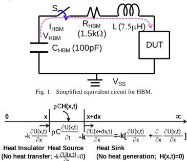
Fig. 1. Simplified equivalent circuit for HBM.
Fig. 2. One dimensional heat conduction through a large plane in a semi-infinite body.
C
HBM(100pF)
R
HBM(1.5k
)
L (
7.5m
H)
DUT
V
HBMS
V
SSI
HBMx x+dx
CH(x,t)
x
U(x,t)
-k 0
t
U(x,t)
C
x
U(x+dx,t)
-
k
=-k[ + ]U(x,t)x
U(x,t)
x
x
Heat Sink Heat Insulator Heat Source
U(x,t)
-k =0 x
III. PHYSICAL MODEL
A. HBM Discharge Current
Fig. 1 shows the simplified equivalent circuit of a device under the HBM event. Compared to the 1.5k resistor, the device Ron is too small. So, the device IHBM can be
approximated to the short circuit HBM current [13].
(1) where
.
Using this equation, the calculated current of a typical snapback device, grounded gate nMOS device (GGNMOS), during the 2kV HBM event (Fig. 3) match to the measurement, clearly demonstrating its validity to describe the device discharge behavior. By neglecting the rising transient, the HBM current of the device after 10ns can be simplified to
(2) where IHBMO=VHBM/RHBM, and m=1/( RHBMCHBM).
Fig. 3. Measured and calculated 0.5kV HBM voltage and current waveforms of the GGNMOS (Total Width=360um in Table I).
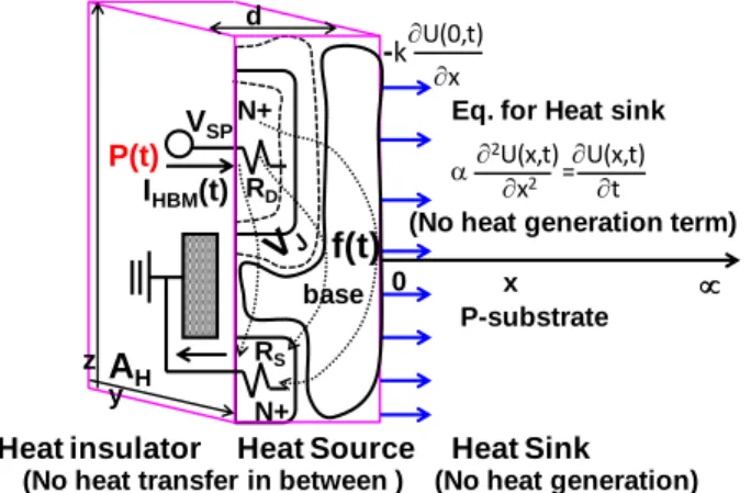
B. Electrothermal Model for HBM and TLP
Fig. 4 schematically illustrates the heat generation and conduction for a device under the HBM event. The heat generation rate can be expressed as P(t)=VSPIHBM(t), where
Vsp is the snapback voltage. Part of the heat is transferred
outside the device by the temperature gradient (-kAU(x,t)/x) and the rest of heat is stored in the device to increase its temperature (CAHdf(t)/t). Based on the law of energy
conservation, the electrothermal equation of the device under the HBM event is
(3) where AHd is the device turn-on volume [14] and assumed as
equal to Adexp(-t) in response to the exponential decay IHBM
from EMMI result in [15], AH is the device turn-on area in the
yz plane, and d is the maximum distance in the normal direction of yz plane (x-axis) that the current flows through.
Without heat generation, the heat equation at the region outside the device from Eq. (1) is
(4)
subject to U(0,t)=f(t), U(x,t)=0, U(x,0)=0
Taking Laplace transformation of Eq. (4), the general solution [16] for the heat equation with semi-infinite region outside the device is
(5) Taking the derivative of T(x,S) at x=0,
(6) Taking Laplace transformation of Eq. (3) and substituting Eq. (2) and Eq. (6) into it yields
m
(7) where PHBM=VSPVHBM/RHBM, =k/(Cd2) and =m-.
This equation also can be obtained by the thermal ohm’s law [17], [18]. The thermal impedance for a device under the voltage or current stress is [19]
(8) In accordance with [19, the "S" term could be adjusted to allow for properties of metal in the heat source layer. Laplace transform of power generation rate P(s) for the device under the HBM event is PHBM/(S+) from Eq. (2) and Eq. (7).
According to the thermal Ohm’s law [17-19], the Laplace transform of temperature for the device under the HBM is
(9) This equation is identical to Eq. (7).
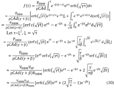
Applying the inverse Laplace transform (L-1
[19], [20], the temperature of the semiconductor
device under the HBM stress is
Let =2,
] (10)
Assuming m=0, Eq. (2) also can be used to depict the current of the device during the TLP stress since it is a square current pulse (Fig. 5). Substituting =0 into Eq. (10) and using ITLP instead of IHBMO (VHBM/RHBM), the temperature of the
device during the TLP stress is obtained as
] (11)
0.00
0.10
0.20
0.30
2
4
6
8
10
12
0
100
200
300
400
Measured Voltage
Calculated Current
Measured Current
V
o
lt
a
g
e
(V)
C
u
rre
n
t
Fig. 4. Schematic depiction of heat generation and conduction for a GGNMOS device under a HBM stress event.
Fig. 5. Voltage and current waveforms of the GGNMOS (total width 360um in Table I) under a 0.12A TLP.
C. Electrothermal Model for Correlation Factor
The main failure mechanism for device during the TLP or HBM stress is the thermal runaway caused when the device temperature reaches the melting point of silicon. Based on this failure criterion (Eq. (10=Eq. (11)), the CF is
(12)
where tT and tH are the times to failures of the device for the
TLP stress and HBM stress with tT=100ns for a 100ns TLP.
IV. MODEL VALIDATION AND DISCUSSIONS
The devices used for validating the newly developed model are: (a) N+ Nickel silicide poly resistor, (b) 2.5V MOFET’s and (c) N+/PW diodes, which are all fabricated on a mature high volume CMOS technology process. Commercial calibrated HBM and TLP testers are used for the experimental evaluations. The TLP tester used a standard 100ns pulse width.
A. W-B Model and New Model Validation
Fig. 6 shows the voltage and current waveforms in silicided N+ poly resistor under a 100ns TLP stress event. Between ~-24ns to 0ns, the pulse travels through the cable from the TLP system to the device under test. When the pulse transient arrives at the resistor (~0ns), the voltage increases from 4.2V to 6.5V due to the impedance mismatch. After this transient, the
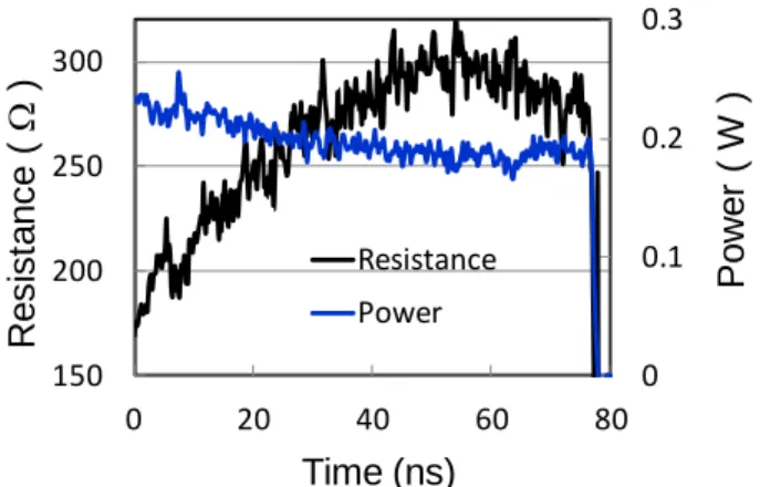
voltage and current change with time, attributed to the Joule-heating induced the resistance change. Fig. 7 shows the time varying resistance (R=V/I) and power (P=VI) based on the measured waveforms in Fig. 6. The resistance increases from 170 to 300 and saturates to 300 between 48ns and 55ns, and then decreases with time. The power only slightly decreases with time (0.22W-0.19W) and therefore can be assumed as a constant for whole stress period. So, this TLP measurement can be used to verify the electrothermal behavior of the resistor against Wunsch-Bell model [7] and the new model since both models assume constant power.
Most resistors fabricated on CMOS technology have positive temperature coefficient below the critical temperature. With this characteristic, the temperature of a resistor under the TLP is T(t)=(R(t)/Ro-1)/ (13)
From the measured resistance in Fig. 7 and Eq. (13), the temperature of silicided N+ poly resistor under the TLP stress is shown in Fig. 8. The temperature increases with time from the room temperature until ~1000C, and then saturates at 1000C after 48ns. The temperature saturation is attributed to loss of silicide (NiSi2) adhesion and it agglomerates into the
polysilicon as the temperature increases to 1000C [21], as confirmed by the TEM image, Fig. 9. This gives a direct physical evidence that the temperature extracted from the measured voltage and current waveforms accurately depict the temperature of the resistor under the TLP stress.
Fig. 8 also confirms that the calculated temperature based on the new model (Eq. (11)) match to the extracted temperature from measurement data below the NiSi2 agglomeration
temperature. However, the calculated temperature based on the W-B model (
) [7] only fits the extracted temperature from measurement data within first 15ns and starts to deviate from the evaluated curve. This demonstrates that new model can depict the thermal behavior of the resistor better than the Wunsch-Bell model, improving the predictability by 3x. Moreover, the similar result also can be seen in Fig. 11 for the resistor under the stress below the thermal runaway (Fig. 10). The calculated temperature based on the new model (Eq. (11)) match to the evaluated temperature within whole stress period, while the Wunsch-Bell model only fits the evaluated temperature within 20ns, again achieving 3x accuracy in the model predictability.
Fig. 6. Voltage and current waveforms of the silicide N+ poly resistor under 100ns TLP pulse for the stress level that can lead to the thermal runaway. VSPN+
N+
P-substrate base
d
0 x
f(t)
x
2U(x,t) U(x,t)
x2
=
t
U(0,t)
-k
P(t)
RD
RS IHBM(t)
Eq. for Heat sink
Heat insulator Heat Source (No heat transfer in between )
(No heat generation term)
A
HHeat Sink (No heat generation) y
z
0 30 60 90 120
0 3 6 9
0 30 60 90 120
Voltage Current
V
o
lt
a
g
e
(V)
C
u
rre
n
t
(mA
)
Time (ns)
Time (ns)
V
o
lta
g
e
(
V
)
C
u
rre
n
t
(
mA
)
0 10 20 30 40
0 2 4 6 8
-30 0 30 60 90
Voltage Current
T
L
P
t
ra
v
e
lin
g
th
ro
u
g
h
c
a
b
le
Fig. 7. Measured resistance and power from the waveforms of the silicide N+ poly resistor under 100ns TLP in Fig. 6.
Fig. 8. Extracted temperature based on measured resistance in Fig. 7 and Eq. (13), and calculated temperatures based on Eq. (11), and Wunsch-Bell (W-B) model for silicide N+ poly resistor under the 100ns TLP in Fig. 6.
Fig. 9. TEM cross-section of silicide N+ poly resistor after 100ns TLP pulse stress event shown in Fig. 6., showing silicide migration from the top film through and mixes with the poly silicon.
Fig. 10.100ns TLP stress voltage and current waveforms on the silicide N+ poly resistor at a stress level below the thermal runaway condition.
Fig. 11.Extracted temperature based on Fig. 10 and Eq. (13), and calculated temperatures based on Eq. (11), and Wunsch-Bell (W-B) model for silicide N+ poly resistor under 100ns TLP in Fig. 10.
B. CF Model Validation by N/PMOS
The TLP generated power in GGNMOS is a constant since the voltage and current are constants within the snapback region (Fig. 5). As such, the temperature of the GGNMOS under the TLP stress event increases with time according to Eq. (11) (Fig. 12). In contrast, the temperature of GGNMOS under the HBM event first increases with time and remains at the highest temperature for a period (~200ns-300ns), and then decreases with time based on Eq. (10). This demonstrates that the time to induce the thermal runaway to damage the device occurred much after the current peak (~10ns in Fig. 3), at which IHBM decreases with a time constant (m).
From Eq. (11), the temperature of device under the TLP stress is function of the device density , specific heat capacity C, TLP current ITLP, snapback voltage VSP, stress time t,
drawing area A, maximum current distance in x-axis d, and which is equal to k/(Cd2
),where k is the thermal conductivity. So, the only unknown parameter in Eq. (11) is “d”. For a device under the It2 stress event, the damage is the thermal
runaway caused by the Joule-heating induced the temperature of the device higher than the silicon melting point (1414C). Through the interactive method, the d can be obtained once the temperature of the device is equal to 1414C at 100ns by substituting the It2, Vt2, , C, k, A, and into Eq. (11). As the d
is obtained, the only one unknown parameter in Eq. (10) is “ ”. Based on similar methodology, the also can be got when the maximum temperature of the device during the HBM stress is equal to 1414C by substituting the It2, Vt2, , C, , A, and
into Eq. (10).
The high current IV characteristics of the devices in Table I under the 100ns TLP stresses are shown in Fig. 13 and Fig. 14. The It2, Vsp and CF (VHBM/It2) of the devices extracted from
Fig. 13 and Fig. 14 and HBM test result are shown in Table I. It can be seen that the CF is not a constant, which varies with the device dimension and the range is from 1.25k to 1.73k. Except the , all parameters in Eq. (10) are unchanged with the device structure. The is the decay time difference (=m-) between the IHBM and device turn-on volume. Since the m is a
constant (1/(RHBMCHBM)=1/150ns) from Eq. (2), the parameter
that is inducing the CF variation with the device structure should be the . Based on Eq. (10), Vsp, VHBM and silicon
melting point, the time varying temperature, , , and CF for the device under the HBM event can be calculated and shown in Fig. 12 and in Table I. It can be seen that the calculated CF’s
Time (ns)
R
e
si
st
a
n
ce
(
)
Po
w
e
r
(
W
)
0 0.1 0.2 0.3
150 200 250 300
0 20 40 60 80
Resistance Power
Time (ns)
T
e
mp
e
ra
tu
re
(
C
)
o
0 200 400 600 800 1000 1200
0 20 40 60
Evaluated New Model W-B Model
0 10 20 30
0 1 2 3 4
-50 0 50 100
Voltage Current
Time (ns)
V
o
lt
a
g
e
(
V
)
C
u
rre
n
t
(
mA
)
T
L
P
t
ra
v
e
lin
g
th
ro
u
g
h
c
a
b
le TLP stress
Time (ns)
T
e
mp
e
ra
tu
re
(
C
)
o
0 200 400 600 800
0 20 40 60
(CF1) are all the same as the measured CF’s. This confirms that the CF varied with the total width (TW) is caused by the . From Table I, the increases as the device TW decreases. This is attributed to the turn-on condition of bipolar IsubRsub0.7V,
which Rsub depends on the position of device (see A or B in Fig.
8) and device TW. As the Isub follows the IHBM to fall, it leads
to the device turning off gradually once that regions cannot satisfy the turn-on criterion. With the smaller Rsub and Isub, the
turn-on area of the smaller TW device (Fig 15) shuts off with the faster speed () as shown in Fig. 16, resulting in the higher stress current density to lead to smaller HBM performance as shown in Table I. It can be seen that the device HBM performance is not proportional to the device TW, while the device It2 is nearly proportional to the device TW since TLP is a constant stress, which does not lead to the device turn-on area varying with time.
Fig. 12.Calculated temperatures of GGNMOS (total width 360um in Table I under the 2.9A and 5.5kV HBM events.
Fig. 13.TLP IV characteristics of GGNMOS devices in Table I.
Fig. 14. TLP IV characteristics of GGPMOS devices in Table I.
Fig. 15. Top view and substrate resistors for different positions of GGMOS devices (total widths 120um and 240um).
Fig. 16.Voltage and current waveforms on various GGNMOS devices under 100V HBM zapping events.
Table I: Measured CF (VHBM/It2) and calculated CF1 (Eq. 12)
for 2.5V GGNMOS/GGPMOS with total width (TW)
MOS TW It2 VHBM CF Vt2 CF1
NMOS 120um 1.2A 1.5kV 1.25k 8.39V 0.79m 0.21m 1.249k
NMOS 240um 2.39A 3.75kV 1.57k 8.32V 0.68m 0.32m 1.568k NMOS 360um 3.59A 5.75kV 1.6k 8.2V 0.66m 0.34m 1.601k PMOS 120um -0.9A -1.3kV 1.4k -11.3V 0.72m 0.28m 1.446k PMOS 240um -1.8A -3.0kV 1.67k -11.8V 0.64m 0.36m 1.668k PMOS 360um -2.6A -4.5kV 1.73k -12.5V 0.61m 0.39m 1.729k Note: m is the decay time constant of IHBM, is the decay time
constant for device turn-on volume in response to IHBM, and is the
decay time difference (=m-) between the IHBM and device turn-on
volumn.
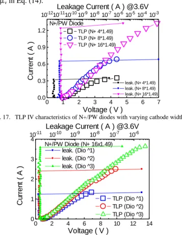
C. CF Model Validation by Diode
Table II shows the layout split, Vt2, It2, VHBM and CF of the
N+/PW diodes for the TLP test results (Fig. 17 and Fig. 18) and HBM test result. It can be seen that the measured CF’s for all diodes in this experiment are almost the same (~1.85k) and is very insensitive to the diode layout.
For a diode under the TLP event, the generated power is a constant since the voltage should be constant in response to a constant current stress. With a constant power, the temperature of the diode under the TLP stress event increases with time
T
e
mp
e
ra
tu
re
(
o
C
)
Time (ns)
0200 400 600 800 1000 1200 1400
0 100 200 300 400
TLP HBM
guard-ring
A
B
D S D
S S S D S D D S D S
guard-ring
A
B
0 20 40 60 80
2 4 6 8 10
0 100 200 300 400
V (120um) V (240um)
V (360um) I (120um)
I (240um) I (360um)
Time (ns)
V
o
lt
a
g
e
(
V
)
C
u
rre
n
t
(
mA
)
0 1 2 3 4
2 3 4 5 6 7 8 9
C
u
rr
e
n
t
(
A
)
Voltage ( V )
TLP (TW 120u) TLP (TW 240u) TLP (TW 360u)
10-10 10-9 10-8 10-7 10-6 10-5 10-4 10-3
Leakage Current ( A ) @ 2.5V
leak, (TW 120u) leak. (TW 40u) leak. (TW 360u)
0 1 2 3
2 4 6 8 10 12
C
u
rr
e
n
t
(
A
)
Voltage ( V ) TLP (TW 120u) TLP (TW 240u) TLP (TW 360u)
10-10 10-9 10-8 10-7 10-6 10-5 10-4 10-3
Leakage Current ( A ) @ 2.5V
according to Eq. (11) (Fig. 20). Although the falling part of the HBM IV curve of a diode can match its TLP IV curve [22], the IV curves in Fig. 17 or Fig. 18 cannot be transferred to the time domain to depict the transient behavior of the diode under the HBM event. It has been illustrated that the voltage of the diode after the peak voltage of the HBM event falls with another decay time (mv) to a constant voltage in response to the
exponential decay HBM current [22] and can be assumed as Vt2(1+exp(-mvt)). So, the power of diode is VHBMVt2
[exp(-mt)+exp(-(m+mv)t)]/RHBM from Eq. (2) and the temperature
equation for N/PMOS (Eq. (10)) can be modified as the equation for diode during the HBM event:
]=T1+T2 (14)
With the similar equation, the temperature of diode under the HBM event increases with time first until reaching the maximum temperature, and then decreases with time as shown Fig. 19. It can be noted that the highest temperature caused by the decay time m (150ns) is nearly at 100ns. Because of one decay time constant (m+mv) longer than 150ns, the highest
temperature of the diode occurs within 100ns, which is between the maximum temperatures caused by the two time constants. Based on Eq. (14) and Eq. (11), the calculated CF for the diode in Fig. 19 is 1.86k. It is very close to the measured CF 1.85k in Table II but different from the HBM output resistance 1.5k. This is caused by that CF is not only function of HBM output resistance and time to failure but also function of the thermal decay times (m-) in Eq. (10) or m and m+mv in Eq. (14).
Fig. 17. TLP IV characteristics of N+/PW diodes with varying cathode width.
Fig. 18. TLP IV characteristics of N+PW diode for various diodes in Table 1.
Fig. 19. Calculated temperatures of the N+/PW diode (area 41.49um2 in
Table II) under the 0.35A TLP and 0.65kV HBM events.
Table II: Measured CF (VHBM/It2) for N+/PW diodes
N+ area(um2) Diode no. Vt2 It2 VHBM CF
41.49 1 3.63V 0.35A 0.65kV 1.85k
81.49 1 3.92V 0.65A 1.2kV 1.84k 161.49 1 6.21V 1.24A 2.3kV 1.85k 161.49 2 9.37V 2.4A 4.5kV 1.87k 161.49 3 11.9V 3.59A 6.8kV 1.89k
V. CONCLUSIONS
The electrothermal behaviors of ESD protection devices have been extensively studied and a novel physical model which is far better than the classic Wunsch-Bell model developed 50 years ago is described. Using one equation, the electrothermal behavior of the traditional ESD devices such as a resistor, diode and snapback device matching to HBM and TLP experimental data can be predicted. The TLP event is the special case of the HBM event, where the RC decay time m is zero. The model is also able to explain physical mechanism of device response under HBM or TLP and the correlation factor (CF) between HBM and TLP stress results for various ESD protection devices.
ACKNOWLEDGMENT
The authors would like to acknowledge the support from their organizations and collaborators. All authors extend their appreciation to the mentor of this paper, Shih-Hung Chen.
REFERENCES
[1] T. J. Maloney, and N. Khurana, “Transmission line pulsing technique for circuit modeling of ESD phenomenon,” in Proc. EOS/ESD Symposium, pp. 49–54, 1985.
[2] C. H. Diaz, T. E Kopley and P. J. Marcous, “Building-in ESD/EOS reliability for sub-halfmicron CMOS processes,” IEEE Trans. on Electron Devices, vol. 43, no. 6, pp. 991–999, Sep. 1996.
[3] D. G. Pierce, W. Shiley, B. D. Mulcahy, K. E. Wanger, and M. Wunder, “Electrical Overstress Testing of a 256K UVEPROM to Rectangular and Double Exponential Pulses,” in Proc. EOS/ESD Symposium, pp. 137– 146, 1988.
[4] S.G. Beebe, “Methodology for Layout Design Optimization of ESD Protection Transistors,” in Proc. EOS/ESD Symposium, pp. 265–275, 1996.
0 200 400 600 800 1000 1200 1400
0 50 100 150 200
T
e
mp
e
ra
tu
re
(
o
C
)
Time (ns)
T (TLP) T1+T2 (HBM)T1 (HBM (m)) T2 (HBM (m+mv))
0.0 0.3 0.6 0.9 1.2
0 1 2 3 4 5 6 7
N+/PW Diode
C
u
rr
e
n
t
(
A
)
Voltage ( V ) TLP (N+ 4*1.49) TLP (N+ 8*1.49) TLP (N+ 16*1.49)
10-1210-1110-1010-910-810-710-610-510-410-3
Leakage Current ( A ) @3.6V
leak. (N+ 4*1.49) leak. (N+ 8*1.49) leak. (N+ 16*1.49)
0 1 2 3 4
0 2 4 6 8 10 12 14
N+/PW Diode (N+ 16x1.49)
C
u
rr
e
n
t
(
A
)
Voltage ( V )
TLP (Dio ^1) TLP (Dio ^2) TLP (Dio ^3) 10-11 10-10 10-9 10-8 10-7 10-6
Leakage Current ( A ) @3.6V
[5] G. Notermans, P. D. Jong, P.Egger, O. Gieser, and C. Musshoff, “Does the ESD-failure current obtained by transmission-line pulsing always correlate to human body model tests?,” in Proc. EOS/ESD Symposium, pp. 4A.7.1–4A.7.7, 1997.
[6] W. Stadler, X. Guggenmos, P.Egger, and F. Kuper, “Pitftalls when correlating TLP. HBM and MM testing,” in Proc. EOS/ESD Symposium, pp. 3A.3.1–3A.3.7, 1998.
[7] D. C. Wunsch, and R. R. Bell, “Determination of Threshold Failure Levels of Semiconductor Diode and Transistor due to Pulse Voltage,”
IEEE Trans. Nuclear Science, vol. 15, pp. 244–259, Dec. 1968. [8] D. M. Tasca, “Pulse Power Failure Modes in Semiconductor,” IEEE
Trans. Nuclear Science, vol. 17, pp. 364–372, Dec. 1970.
[9] D. L. Lin, “Thermal Breakdown of VLSI by ESD Pulses,” in Proc. Int. Rel.Phys. Symp. (IRPS), pp. 281–287, 1990.
[10] P. Salome, C. Leroux, P. Crevel, J. P. Chante, “Investigations on the Thermal Behavior of Interconnects under ESD Transients using a Simplified RC Network,” in Proc. EOS/ESD Symp., 1998, pp. 3A.5.1– 3A.5.12.
[11] V. M. Dwyer, A. J. Franklin and D. S. Campbell, “Thermal Failure in Semiconductor Devices,” Solid-State Electronics, vol. 33, pp. 553–560, 1990.
[12] Y. Cao, U. Glaser, J. Willemen, F. Magrini, “ESD Simulation with Wunsch-Bell based Behavior Modeling Methodology,” in Proc. EOS/ESD Symp., 2011, pp. 1–10.
[13] J. H. Lee, Natarajan M. Iyer., “Analyitcal Model of Correlation Factor for Human Body Model to Transmission Line-PulseESD Test,” IEEE Elec. Dev. Letters, vol. 38, no. 7, pp. 952–954, Jul. 2017.
[14] J. H. Lee, Natarajan M. Iyer., R. Jain and M. Prabhu, “Predictive High Voltage ESD Design Methodology,” in Proc. EOS/ESD Symposium, pp. 1A.3.1–1A.3.8, 2016.
[15] J. H. Lee, K. M. Wu, S. C. Huang, C. H. Tang, “The Dynamic Current Distribution of a Multi-Fingers GGNMOS under High Current Stress and HBM ESD Events,” in Proc. Int. Rel.Phys. Symp. (IRPS), pp. 629– 630, 2006.
[16] Web
http://www.math.umbc.edu/~jbell/pde_notes/12_SemiInfiniteDomains.p df
[17] T. J. Maloney, L. Jiang, S. S. Poon, K. B. Kolluru, and AK.M Ahsan, “Achieving Electrothermal Stability in Interconnect Metal during ESD Pulses,” in Proc. Int. Rel.Phys. Symp. (IRPS), 2013, EL-1.
[18] T. J. Maloney,“Modeling Feedback Effects in Interconnect Metal under ESD Stress,” in Proc. Int. Rel.Phys. Symp. (IRPS), pp. 6A-4.1-6A-4.6, 2016.
[19] T. J. Maloney,“Unified Model of 1-D Pulsed Heating, Combining Wunsch-Bell with the Dwyer Curve,” in Proc. EOS/ESD Symp., pp. 3A5.1-3A5.12, 2016.
[20] Web http://eqworld.ipmnet.ru/en/auxiliary/inttrans/laplace7.pdf [21] M. Tinani, M. Mueller, Y. Gao, and E. A. Irene, Y. Z. Hu, and S. P. Tay
“In Situ Real-Time Studies of Nickle Silcilide Phase Formation,” J. Vac. Technol., pp. 376–383, 1990.