Frequency conversion in
two-dimensional photonic structures
Publisher: Casimir Research School, Delft, the Netherlands
Cover Design: Aileen Kartono
Frequency conversion
in
two-dimensional photonic structures
PROEFSCHRIFT
ter verkrijging van
de graad van Doctor aan de Universiteit Leiden,
op gezag van Rector Magnificus prof. mr. P. F. van der Heijden, volgens besluit van het College voor Promoties
te verdedigen op dinsdag 17 mei 2011 klokke 13:45 uur
door
Ljubiša Babić
Promotiecommissie:
Promotor: Prof. Dr. J. P. Woerdman Universiteit Leiden Copromotor: Dr. M. J. A. de Dood Universiteit Leiden
Leden: Prof. Dr. J. Gómez Rivas Technische Universiteit Eindhoven Prof. Dr. H. W. M. Salemink Technische Universiteit Delft Dr. Ir. T. H. Oosterkamp Universiteit Leiden
Prof. Dr. D. Bouwmeester Universiteit Leiden en University of California at Santa Barbara (UCSB) Prof. Dr. E. R. Eliel Universiteit Leiden Prof. Dr. J. M. van Ruitenbeek Universiteit Leiden
The work presented in this thesis has been made possible by financial support from the Dutch Organization for Scientific Research (NWO) and is part of the scientific program of the Foundation for Fundamental Research of Matter (FOM).
An electronic version of this dissertation is available at the Leiden University Repository (https://openaccess.leidenuniv.nl).
Contents
1 Introduction 1
1.1 Photonic structures . . . 1
1.1.1 Photonic crystals . . . 1
1.1.2 Nanowires . . . 4
1.2 Frequency conversion . . . 5
1.3 Thesis outline . . . 6
2 Second harmonic generation in gallium phosphide nanowires 11 2.1 Introduction . . . 11
2.2 Sample description . . . 12
2.3 Setup . . . 15
2.3.1 Description of the setup . . . 15
2.3.2 Second harmonic generation from BBO . . . 17
2.4 SHG in samples with GaP nanowires . . . 19
2.4.1 Tensor properties of nanowires . . . 20
2.4.2 Second harmonic generation at 425 nm . . . 24
2.5 Conclusion . . . 25
3 Second harmonic generation in freestanding AlGaAs photonic crystal slabs 27 3.1 Introduction . . . 27
3.2 Fabrication of photonic crystals . . . 29
3.3 Setup . . . 32
Contents
3.3.2 Second harmonic generation . . . 34
3.4 Linear optical characteristics . . . 34
3.5 Nonlinear optical properties . . . 42
3.6 Conclusion . . . 48
4 Method to transfer photonic crystals to a transparent gel sub-strate 51 4.1 Introduction . . . 51
4.2 Sample preparation . . . 53
4.3 Experiment . . . 57
4.4 Results and Discussion . . . 57
4.4.1 Leaky modes of photonic crystal slabs before and after the transfer to the gel substrate . . . 57
4.4.2 Interaction between the leaky modes of photonic crystal slabs transferred to a gel substrate . . . 61
4.5 Conclusions . . . 68
5 Interpretation of Fano lineshape reversal in the reflectivity spectra of photonic crystal slabs 71 5.1 Introduction . . . 71
5.2 Experiment . . . 73
5.3 Results . . . 74
5.4 Discussion . . . 76
5.4.1 Scattering matrix formalism . . . 78
5.4.2 Example: 2-port asymmetric slab . . . 80
5.4.3 Asymmetry reversal with nonzero background . . . 84
5.5 Conclusions . . . 90
6 Second harmonic generation in transmission from photonic crystals on a gel substrate 91 6.1 Introduction . . . 91
6.2 Sample preparation . . . 93
6.3 Experiment . . . 94
6.4 Results and discussion . . . 96
6.5 Conclusions . . . 107
Bibliography 109
Summary 117
Contents
Curriculum Vitæ 125
List of publications 127
Chapter 1
Introduction
1.1
Photonic structures
Photonic structures that show features on a wavelength or even subwavelength scale are widespread in nature. For example, the wings ofMorphobutterflies, the scales of the Brazilian beetleLamprocyphus augustus, and opal gemstones all derive their iridescent colors from variations in the refractive index on a microscopic scale, comparable to the wavelength of visible light. The shim-mering blue color of the Morpho butterfly, the sparkling green color of the Brazilian beetle, and attractive iridescent colors of an opal gemstone are to a large extent produced by their internal structure, not by pigments [1–3]. Over the course of millions of years, life has evolved to make nanostructures of astonishing complexity that exhibit striking optical properties [4]. Slowly, but with great determination, human beings are catching up with Nature by ar-tificially creating nanostructures with wavelength and subwavelength feature sizes in materials with a high refractive index.
1.1.1 Photonic crystals
In 1987, Eli Yablonovitch [5] and Sajeev John [6], independent from each other, proposed a novel type of periodic photonic structures called photonic crystals to control the propagation of light. Yablonovitch proposed to inhibit sponta-neous emission of an atom placed inside these structures, while John predicted that photonic crystals can be used to localize light in three dimensions.
1. Introduction
(800–900 nm) were realized [8]. Today, photonic crystals are recognized as structures that can tailor the propagation of light in a unique way and provide enhanced light-matter interaction. As such, photonic crystals find application in lasers, single photon emitters, waveguides, filters, frequency convertors, nonlinear switches, sensors, and slow-light media [9–11].
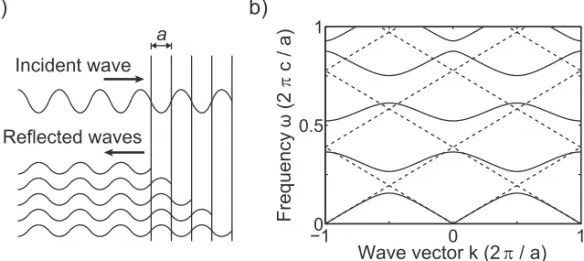
Propagation of light in a photonic crystal is analogous to the propagation of electrons in a semiconductor crystal. Figure 1.1(a) shows constructive inter-ference of light waves reflected from a one-dimensional periodic structure with a spatial perioda. For an appropriate frequency of lightω, the reflected waves from all the interfaces are in phase and the interference is constructive, similar to Bragg reflection of X-rays from a crystalline solid [12]. When this Bragg condition is met, light is totally reflected, and it cannot propagate through the structure. For a realistic photonic structure with a finite index contrast the Bragg peaks are significantly broadened and form frequency ranges for which the propagation of light in the periodic structure is forbidden in a particular direction. These forbidden gaps, called photonic stop gaps or photonic band gaps, can be described by a photonic band structure.
Figure 1.1(b) shows the photonic band structure (frequencyωas a function
a) b)
Incident wave
Reflected waves a
−10 0 1
0.5 1
Wave vector k (2 π / a)
Frequency
ω
(2
π
c / a)
1.1 Photonic structures
of the wave vector k) for light waves propagating through a one-dimensional photonic crystal along the direction of periodicity. The structure has a spatial periodaand consists of alternating layers of materials with refractive indices of n1 = 1 (air) and n2 = 3.5, and equal thicknesses d1 =d2 =a/2. The fre-quency ω and the wave vector k are plotted in dimensionless units ωa/(2πc) and ka/(2π), respectively. As can be seen, the photonic band structure re-peats every reciprocal lattice vectorG= 2π/adue to periodicity of the struc-ture. The discrete translational symmetry of the structure conserves the wave vector k modulo the addition of reciprocal lattice vectors, i.e., k=k±mG, wherem is an integer. The region of non-redundant values of wave vector k, −π/a < k≤π/a, is called the first Brillouin zone.
For comparison, the dispersion relation of a homogeneous dielectric mate-rial with a refractive index equal to the effective refractive index of the photonic crystal (ω =ck/nef f) is also shown in the figure with dashed lines. Here,nef f
is equal to the volume average of the dielectric constants of the constituent materials of the multilayer structure. For the periodic structure discussed here
nef f = 2.6. The dispersion relation of the homogeneous dielectric is repeated
every reciprocal lattice vectorG. As can be seen, the propagation of light in a photonic crystal is very different from the propagation of light in a homoge-neous dielectric material. In a photonic crystal, light can be slowed down close to the edges of the first Brillouin zone (k=±π/a) or forbidden to propagate through the structure. By tuning the period (a), thicknesses of the layers (d1 andd2), and refractive indices of the layers (n1 andn2), it is possible to tune the dispersion of light in a photonic crystal.
1. Introduction
1.1.2 Nanowires
Semiconductor nanowires are one-dimensional nanostructures that can be epi-taxially grown using small, typically subwavelength, gold particles as a cat-alyst [13]. The actual nanowire grows under the gold particle and typical, as-grown wires, have a diameter of a few tens of nanometers and can be sev-eral micrometers long. The optical and electrical properties of the wires may be tuned by controlling their growth. Both regular and random arrays of nanowires as well as single nanowires can be grown for nanowire-based opto-electronic devices that include lasers [14–16], waveguides [17, 18], photodetec-tors [19–21], solar cells [22, 23], nonlinear optical converters [24, 25], biological and chemical sensors [26].
1.2 Frequency conversion
1.2
Frequency conversion
Frequency conversion refers to a process in which the incoming radiation generates radiation at a different frequency by interacting with a nonlinear medium [29]. This nonlinear process can be used to generate coherent radia-tion in the spectral regions where there are no convenient laser sources [30]. For instance, sum frequency generation can be used to produce tunable ra-diation at ultraviolet wavelengths by mixing the output of a fixed-frequency visible laser and the output of a frequency-tunable visible laser. The gener-ated radiation can be used in biomedical applications because most organic materials absorb in the ultraviolet region. Difference frequency generation can be used to obtain tunable mid-infrared coherent radiation in the wavelength range of 3–12µm. Since most molecules in the atmosphere have their strong absorption lines in this wavelength region, the mid-infrared radiation can be used for remote sensing of the atmosphere.
Besides practical applications, the process of frequency conversion is of great interest for fundamental science as well. A pump photon from an in-tense blue laser can spontaneously produce two photons at a red wavelength via a process called spontaneous parametric down-conversion. Since these twin photons are generated in pairs, strong correlations exist between the photons. Under appropriately chosen conditions this may lead to the gener-ation of entangled photon pairs, which can be used to test the fundamental laws of quantum mechanics.
In this thesis we will constrain ourselves to the particular case of second harmonic generation (SHG), also known as frequency doubling. This is a relatively strong second-order nonlinear process that exists only in materials where the inversion symmetry is broken. These materials show a nonzero second-order nonlinear coefficientd.
1. Introduction
materials such as beta-barium borate (BBO), potassium titanyl phosphate (KTP), or lithium niobate (LiNbO3) [29]. However, this solution excludes op-tically isotropic materials with a much larger second-order nonlinearity. For example, the nonlinear coefficients dof gallium arsenide (GaAs) and gallium phosphide (GaP) are respectively about 70 and 30 times larger than the coef-ficientdof a BBO crystal [31, 32].
Bloembergen et al. [33] were the first to propose a periodic photonic struc-ture with alternating layers of GaP and GaAs as a way to satisfy the phase-matching condition in III-V materials. By a proper choice of the parameters of the multilayer structure the dispersion of light can be tuned in such a way that the waves at the fundamental and the second harmonic frequency are phase-matched (∆k= 2k(ω)−k(2ω) = 0). Furthermore, an existing phase mis-match in a periodic structure can be compensated by adding an appropriate re-ciprocal lattice vector of the photonic lattice (∆k= 2k(ω)−k(2ω) +mG= 0). This latter mechanism is called quasi-phase-matching.
To summarize, we identify three different mechanisms by which a photonic structure can reduce a phase mismatch in a nonlinear optical process:
(i) Form birefringence, related to the anisotropy of the fundamental build-ing blocks of the structure, can reduce a phase mismatch if different polarization states are used.
(ii) The strong light-matter interaction for materials with a large index con-trast gives additional dispersion. This additional dispersion is due to a combination of Bragg diffraction leading to standing wave patterns and waveguide dispersion [34] that originates from the vertical confinement. Both contributions may be tuned via design of the structure.
(iii) In periodic structures discrete translational symmetry conserves the wave vector modulo the addition of a reciprocal lattice vector. This leads to quasi-phase-matching and allows to add a reciprocal lattice vector to the phase mismatch.
1.3
Thesis outline
1.3 Thesis outline
aluminum gallium arsenide (AlxGa1−xAs) photonic crystal slabs in Chapters
3–6 and ensembles of aligned gallium phosphide (GaP) nanowires randomly grown in two dimensions in Chapter 2. All the chapters can be read indepen-dently of each other. A short description of each chapter is given below.
• Chapter 2: Ensembles of aligned gallium phosphide nanowires ran-domly grown on a gallium phosphide substrate show strong birefringence originating from the optical anisotropy of the wires. In this chapter we investigate if this birefringence can be used to reduce the phase mismatch in the nonlinear process of second harmonic generation. We describe a number of experiments that aim at separating the second harmonic light generated by the wires from the second harmonic light generated by the substrate. However, we were not successful in separating the nanowire contribution and showing the effect of the reduced phase mismatch for nanowires that are shorter than the coherence length.
• Chapter 3: This chapter describes the fabrication of freestanding, two-dimensional photonic crystal slabs made in Al0.35Ga0.65As. Light can resonantly couple to leaky modes of these structures, and the dispersion relations of these resonances can be extracted from the measured linear reflection spectra. The nonlinear reflection spectra show that resonant coupling of a pulsed laser at a wavelength of 1.535 µm can significantly enhance the second harmonic signal. By tuning the angle of incidence the pulsed laser beam is tuned into resonance with one of the leaky modes of the structure, and a second harmonic enhancement of more than 4500 ×the non-resonant contribution is measured.
• Chapter 4: A novel method to transfer freestanding photonic crystal slabs to a transparent gel substrate is presented in this chapter. Com-pared to the freestanding structures of Chapter 3, transferred structures allow for both reflection and transmission measurements. The resonant features in measured reflection spectra of a structure on the gel are much more prominent than those in reflection spectra of a freestanding struc-ture. We show that the measured quality factor of one of the leaky modes, Q= 300, is limited by the finite size of the ∼300×300µm2 photonic crystal slab.
1. Introduction
the Fano model. Within this model, the interference between the non-resonant and the non-resonant contribution leads to the asymmetric line-shape in the spectra. For lossless and symmetric structures, the sign of the real-valued parameterqof the Fano model, which can be interpreted as the ratio between the resonant and the non-resonant contribution, controls the asymmetry of the resonance. For a symmetric air-slab-air structure parameter q changes its sign if the amplitude reflection coef-ficient of the slab goes through zero. We show that for an asymmetric air-slab-gel structure it is also possible to change the asymmetry of a res-onance by angle tuning without reaching the condition of zero amplitude. This behavior requires a complex-valued q parameter and demonstrates that a complex q is not necessarily a sign of the microscopic processes of decoherence and/or dephasing.
1.3 Thesis outline
Chapter 2
Second harmonic generation in
gallium phosphide nanowires
2.1
Introduction
Semiconductor nanowires are essentially one-dimensional (1D) nanostructures that have subwavelength lateral dimensions and typical lengths of several mi-crometers. Since the introduction of nanowires by Yazawa et al. [35], many advances have been made in tuning their electrical and optical properties by controlling their growth. Today, nanowires represent a class of metamate-rials that shows promise for many device applications compatible with on-chip technologies. The list of nanowire-based optoelectronic devices includes lasers [14–16], waveguides [17, 18], photodetectors [19–21], solar cells [22, 23], nonlinear optical converters [24, 25], biological and chemical sensors [26].
The high length-to-width aspect ratios of the nanowires combined with the high refractive index of semiconductors can lead to strong polarization anisotropy that facilitates some of their applications. Wang et al. [19] were the first to experimentally demonstrate the optical anisotropy of a single indium phosphide (InP) nanowire by measuring its photoluminescence (PL) proper-ties. The authors point out the possibility of using InP nanowires as polariza-tion sensitive photodetectors incorporated into photonic-based circuits.
nanostruc-2. Second harmonic generation in gallium phosphide nanowires
turing bulk materials represents an important approach in making III-V ma-terials, like gallium arsenide (GaAs) and GaP, more attractive for nonlinear optics [28, 37].
A large optical nonlinearity as well as perfect phase-matching conditions are necessary in order to achieve large nonlinear yields [29]. Phase matching ensures that all the waves generated inside the nonlinear medium interfere con-structively. In most materials, this phase-matching condition is not met due to material dispersion. Therefore, birefringent materials are commonly used to compensate material dispersion and phase-match the nonlinear interaction. Although bulk GaP has about 30 times larger effective second-order nonlinear susceptibility, χ(2)ef f, than that of a BBO crystal, it doesn’t possess birefrin-gence. The second harmonic (SH) signal, generated in bulk GaP, is much smaller than that of bulk BBO. The large geometrical anisotropy of aligned GaP nanowires, combined with a high refractive index contrast between the GaP and the surrounding air, gives rise to strong form birefringence and has been extensively studied by Muskens et al. [27, 36]. However, little is known about using the birefringence of these photonic metamaterials to achieve phase matching in nonlinear optical processes.
In this chapter we study second harmonic generation (SHG) in samples containing ensembles of aligned GaP nanowires randomly grown on a GaP substrate. We investigate the influence of the birefringence of the nanowire layer on second harmonic generation. We consider the symmetry of the second-order nonlinear tensorχ(2) of the nanowire metamaterials as well. The sym-metry of the nonlinear tensor χ(2) of the nanowires maybe differs from that of bulk GaP due to the numerous stacking faults in the nanowires [13].
2.2
Sample description
2.2 Sample description
(b) (a)
1µm
(c)
1µm 1µm
Figure 2.1. Cross-sectional SEM images of aligned GaP nanowires epitaxially grown on a (111)B GaP substrate, with a length of
≈ 1.3 µm and lateral shell growth times of 100 sec. (a), 350 sec. (b) and 1100 sec. (c) [38].
GaP (100) 35
<111>
Figure 2.2. A schematic presentation of the nanowire growth on a (100) GaP substrate. Nanowires grow preferentially along the <111>B directions.
in-2. Second harmonic generation in gallium phosphide nanowires
Figure 2.3. Birefringence (∆n) at a wavelength of 632.8 nm, as a function of the nanowire volume fraction (f), for GaP nanowires grown on a (111)B oriented GaP substrate. The theoretical curve (red line), calculated using Maxwell-Garnet effective medium theory, is plotted on top of the experimental data (points) taken from Ref. [27].
creases strongly with volume fraction reaching values as large as 0.79±0.07 for a volume fraction of 0.4±0.05.
The layer of subwavelength GaP nanowires grown on a (111)B gallium phosphide substrate can be treated as a positive uniaxial crystal. The bire-fringence ∆n=ne−no, with the ordinary (no) and the extraordinary (ne)
index of refraction, is positive, reflecting the stronger interaction with light when theE-field vector is parallel to the long axis of the wires. We approxi-mate the nanowires by infinitely long cylindrical pillars, and assume that the nanowire volume fractionf is low, and use Maxwell-Garnett effective medium theory [39, 40] to calculate the refractive indicesno andne using the following
expressions:
n2o=
1 + 2f α 1−f α
, (2.1)
n2e =f n2+ (1−f), (2.2)
2.3 Setup
The nanowires that we studied all have a similar length of ≈1.3µm, but different samples have different volume fractions f. The wires are grown on ∼500µm thick (111)B oriented substrates. The relevant parameters of sam-ples B9138 (Fig. 2.1(b)) and B9165 (Fig. 2.1(c)) are summarized in Table 2.1.
Table 2.1. Parameters of the nanowire metamaterials used in our ex-periments.
Sample GaP substrate Length Volume fraction f Birefringence
label orientation (µm) (%) ∆n
B9138 (111)B 1.26 15 0.34
B9165 (111)B ≈1.3 40 0.79
2.3
Setup
2.3.1 Description of the setup
Figure 2.4(a) shows a schematic of the setup used to study second harmonic generation in transmission from ensembles of aligned GaP nanowires. A Q-switched diode-pumped solid state laser (Cobolt Tango) is employed as the source of radiation at the fundamental wavelength. The laser uses an Er:Yb-doped glass as the gain medium to produce a laser beam operating in the TEM00 mode (M2<1.2). The fundamental beam has a specified center wave-length of 1535±1 nm and a narrow linewidth (<0.04 nm). Short pulses, with a duration of ≈ 3.8 ns (full width at half maximum) and a ∼1.3 kW peak power, are generated at a repetition rate of 5 kHz.
The divergent laser beam is collimated by lens L1 with a focal length of 60 mm and sent through an optical isolator (OFR IO-4-1535-HP-Z) to eliminate instability of the laser power output due to the optical feedback. During the measurements, we check for laser power fluctuations by monitoring the output of the internal laser photodiode using a Lab View program.
2. Second harmonic generation in gallium phosphide nanowires
SPECTROMETER
LASER BEAM a)
b)
d
SAMPLE OPTICAL
ISOLATOR
POLARIZER SAMPLE ANALYZER
L1 L2 L3 L4
LASER
/2 PLATE
F
IB
E
R
Figure 2.4. (a) Setup used for investigating the second harmonic gen-eration in transmission from nanowire metamaterials. The fundamental beam is focused on the sample and the generated second harmonic is collected in transmission and forwarded to a fiber-coupled spectrometer. Lenses L1–L4 serve to focus and collimate the light. The polarization of the incident fundamental is defined using a combination of aλ/2 plate and a polarizer. The polarization state of the second harmonic is stud-ied with a second polarizer (analyzer). An optical isolator is employed to prevent optical feedback caused by the light reflecting back into the laser cavity. (b) Details of the sample stage. The angle of incidence
θ, the azimuthal angleϕ, and the position of the sampled, can be set individually using motorized stages.
2.3 Setup
2.3.2 Second harmonic generation from BBO
In order to test the setup and our 1535 nm laser we generated second harmonic using a 1 mm BBO crystal. Figure 2.5 shows the measured second harmonic signal as a function of angle of incidence (black dots). The phase matching in this standard crystal is well-known. For a collinear second harmonic generation the power at the SH frequencyP(2ν) is proportional to the square of the power at the fundamental frequencyP(ν), and can be expressed as [29]:
P(2ν)∝L2sinc2(∆kL/2)P(ν)2, (2.3)
where
sinc2(∆kL/2) = sin
2(∆kL/2)
(∆kL/2)2 , (2.4)
and
∆k= 2k(ν)−k(2ν) = 4πν
c (n(ν)−n(2ν)). (2.5)
-6 -4 -2 0 2 4
Angle of incidence (degrees)
0.0 0.5 1.0 1.5x10⁴
Second harmonic power (counts)
-6 -4 -2 0 2 4
0 200 400 600 800
Angle of incidence (degrees)
SH power (counts)
2. Second harmonic generation in gallium phosphide nanowires
Herek(ν) andk(2ν) are the wave vectors at the fundamental and the second harmonic frequency, respectively. Thickness of the crystal is denoted by L. When the refractive index at the fundamental frequency (n(ν)) is equal to the refractive index at the SH frequency (n(2ν)), ∆k= 0 and the phase-matching condition is satisfied resulting in maximum SH yield. For a BBO crystal, phase matching can be achieved by choosing the polarization of the SH wave to be extraordinary so that it experiences the lower of the two refractive indices. We employ type II phase matching where one of the waves at the fundamental frequency is an extraordinary wave while the other wave is an ordinary wave. The phase-matching condition ∆k= 0 can then be expressed as:
no(ν) +ne(ν, ψ)−2ne(2ν, ψ) = 0, (2.6)
whereψis the angle between the wave vectorkand the optic axis of the BBO crystal. The refractive indexne(ν, ψ) is given by
1
ne(ν, ψ)2
= sin
2ψ
ne(ν,90◦)2
+ cos 2ψ
no(ν)2
. (2.7)
In the experiment, the fundamental beam is polarized under an angle of 45◦ with respect to the plane containing the wave vector k of the incident light and the optic axis. The crystal is cut so that the type II phase-matching condition is satisfied close to normal incidence. The fundamental beam is focused to a spot of ≈ 120 µm with a numerical aperture (NA) ≈0.01, and the angle of incidenceθ is varied from -7◦ to 4◦ in steps of 0.1◦. By varying the angle of incidenceθ we vary the angle ψ between the wave vector k and the optic axis.
To fit the experimental data, we use Equation 2.3 with A=L2P(ν)2 as a fitting parameter. The phase mismatch ∆k is given by the known refractive indices of BBO:
∆k= 2πν
c (no(ν) +ne(ν, ψ)−2ne(2ν, ψ)). (2.8)
2.4 SHG in samples with GaP nanowires
2.4
SHG in samples with GaP nanowires
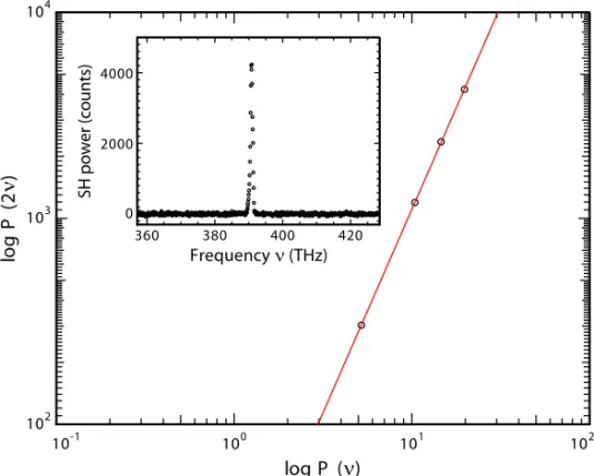
Figure 2.6 shows the measured power of the signal at a frequency of 390.9 THz (wavelength of 767.5 nm) as a function of the power of the incident fundamen-tal beam (black dots), generated in transmission from sample B9165. The inset shows a typical spectrum of the signal detected by a fiber-coupled spec-trometer USB4000. We focus the fundamental beam to a spot of ≈ 120 µm with a numerical aperture≈ 0.01, and keep the angle of incidence as well as the polarization of the incident fundamental constant throughout the measure-ment. The power at the second harmonic frequency grows with the square of the fundamental power, as indicated in Fig. 2.6 with a linear fit (red line) of a slope of 1.975±0.008.
The crucial question is whether this second harmonic signal is generated in the nanowire layer or in the underlying substrate. One possibility is to use the birefringence of the nanowires to achieve phase matching via angle tuning of
10-1 100 101 102
log P (ν)
102 103 104
lo
gP
(2
ν
)
360 380 400 420
Frequency
0 2000 4000
SH power (counts)
(THz)
ν
2. Second harmonic generation in gallium phosphide nanowires
the sample. When successful, a much more efficient SHG would be obtained from the nanowire layer than from the substrate. Unfortunately, it is not possible to demonstrate this with short nanowires with a length of≈1.3µm, which is smaller than the coherence lengthLc. This coherence length is defined
asLc= 2/∆k [29], where ∆k is given by Equation 2.5, and defines a length
over which the fundamental and second harmonic waves are in phase. For a bulk GaP crystal used for frequency doubling of 1535 nm light, the coherence lengthLc is about 3 µm. The large value of ∆k for bulk GaP is due to the
strong dispersion of the material. For a nanowire layer that contains mostly air, the effective refractive index and consequently also the dispersion are lower than that of the bulk. Therefore, we expect a smaller ∆k and thus a longer coherence length. Phase matching which reduces ∆k and increasesLcis only
effective if the crystal thickness L is much larger than Lc (L >> Lc). To
enhance the second harmonic signal due to the nanowires by phase matching, we could make the nanowires much longer than the coherence length. However, long nanowires (> 10 µm) have a significantly reduced birefringence due to the bending of the wires [27]. Therefore, a sample with these long nanowires is not a good candidate for efficient second harmonic generation.
In the remainder of the chapter we will discuss two possibilities to find out whether the measured second harmonic signal in Figure 2.6 is generated in the nanowire layer or in the underlying substrate. In Section 2.4.1 we discuss a possible difference in tensor properties ofχ(2) between the bulk material and the nanowires. In Section 2.4.2 we discuss an experiment where we use the strong absorption of blue light in GaP to get rid of the substrate contribution.
2.4.1 Tensor properties of nanowires
Figures 2.7(a) and (b) show polar plots of the measured SH signal in trans-mission as a function of the azimuthal angleϕfor sample B9165 and a (111) oriented GaP reference substrate, respectively. The experimental data are off-set by 500 counts for clarity. The fundamental beam is at normal incidence, and is focused to a spot of≈120µm with a numerical aperture ≈0.01. The azimuthal angleϕ (Fig. 2.4(b)) is varied from 0◦ to 360◦ in steps of 3◦. The black dots and red triangles in Figure 2.7 correspond to the experimental data points for the parallel and the orthogonal orientation of the polarizer and the analyzer. In this way we probe some of the symmetry properties of the nonlinear susceptibility tensorχ(2).
2.4 SHG in samples with GaP nanowires 2000 4000 0 2000 4000
SH power (counts)
180 150
120 90 60
30 ϕ=0 330 210 270 300 240 180 150
120 90 60
30 ϕ=0 330 210 270 300 240 a) b)
Figure 2.7. Measured SH power as a function of the azimuthal angleϕ
for (a) sample B9165 and (b) a (111) oriented GaP reference substrate, offset by 500 counts for clarity. The SH signal is measured in trans-mission at normal incidence. Black dots (red triangles) correspond to experimental data points for the parallel (orthogonal) orientation of the polarizer and the analyzer (Fig. 2.4(a)). Solid lines serve only as a guide to the eye. As expected, the power at the SH frequency is proportional to sin2(3ϕ) (cos2(3ϕ)).
microscopy (HRTEM) [36]. At the same time, the crystal structure of the nanowires contains many stacking faults [13]. To understand the nature of these defects let us consider the stacking sequence of atomic layers in a cu-bic zincblende structure [12]. In a perfect zincblende structure the atomic layers are stacked in an ...ABCABC... (fcc) sequence along the [111] direc-tion. A stacking fault of the hexagonal layers locally changes the stacking sequence to ...ABAB... (hcp), and as a result a hexagonal wurtzite crystal structure is formed. For GaP nanowires that grow along a [111] direction of the cubic lattice, the wurtzite domains are oriented along a [0001] direction of the hexagonal lattice [12]. The wurtzite structure belongs to a 6mmpoint group symmetry, and has a different second-order nonlinear susceptibility ten-sor compared to a zincblende structure. To appreciate the difference we use a contracted notation for the nonlinear susceptibility tensor. Instead of the rank 3 tensor χ(2) we use a 6×3 rank 2 tensor d with elements dij [29].
For zincblende (group ¯43m) the elements d14, d25, and d36 are all equal and nonzero. For wurtzite (group 6mm) the nonzero elements are d15 = d24,
d31=d32, and d33.
2. Second harmonic generation in gallium phosphide nanowires
the fundamental beam. Instead investigating a system in which the sample is rotated, we study an equivalent problem where both the incident polarization of the fundamental and the analyzer are rotated by the same angle ϕ while the sample is fixed.
The nonlinear polarization PN L(2ν) generated by the electric field E(ν) in the medium is given by [29]
PN L(2ν) = 4d14
Ey(ν)Ez(ν) Ex(ν)Ez(ν) Ex(ν)Ey(ν)
, (2.9)
whereEx(ν), Ey(ν), andEz(ν) are the electric field components along thex, y, andz-axis of the Cartesian coordinate system, respectively. Here, we define
x, y, and z-axis to coincide with the crystallographic axes [100], [010], and [001].
We chose unit vectors √1
2(1,−1,0), 1
√
6(1,1,−2), and 1
√
3(1,1,1), denoted bye1,e2, ande3, respectively, to form an orthonormal basis ofR3. At normal incidence, the wave vectorkof the incident fundamental is parallel toe3 with the E-field in the plane spanned by e1 and e2. Consequently, the incident electric fieldE(r, t) as a function of the azimuthal angleϕis given by
E(r, t) =E(ν, ϕ)e−i2πνt+E(−ν, ϕ)e+i2πνt, (2.10)
where
E(ν, ϕ) = 1 2E0e
ikr(cos(ϕ)e
1+ sin(ϕ)e2)
= 1
2E0e
ikr
cos(√ϕ)
2 +
sin(√ϕ) 6 sin(√ϕ)
6 −
cos(√ϕ) 2 −q2
3sin(ϕ) . (2.11)
Here,E(−ν, ϕ) is the complex conjugate ofE(ν, ϕ), andE0 is the amplitude of the electric field. Combining Equations 2.9 and 2.11, we arrive to the following expression for the Cartesian components of the nonlinear polarizationPN L(2ν) as a function of the azimuthal angleϕ:
PxN L(2ν, ϕ) = 23E2
0d14sin(ϕ)
√
3 cos(ϕ)−sin(ϕ),
PyN L(2ν, ϕ) = −2 3E
2
0d14sin(ϕ)
√
3 cos(ϕ) + sin(ϕ),
PzN L(2ν, ϕ) = −1 3E
2
0d14(1 + 2 cos(2ϕ)).
2.4 SHG in samples with GaP nanowires
The measurement scheme with the parallel (orthogonal) orientation of the polarization of the incident fundamental and the analyzer, filters through the nonlinear polarizationPkN L(2ν, ϕ) (P⊥N L(2ν, ϕ)), given by
PkN L(2ν, ϕ) = PN L(2ν) (cos(ϕ)e1+ sin(ϕ)e2)
= −
r 2 3E
2
0d14cos(3ϕ), (2.13)
P⊥N L(2ν, ϕ) = PN L(2ν) (sin(ϕ)e1−cos(ϕ)e2)
= r
2 3E
2
0d14sin(3ϕ). (2.14)
The corresponding expressions for the SH power as a function of the azimuthal angle ϕ, Pk(2ν, ϕ) and P⊥(2ν, ϕ), are proportional to the square of the
non-linear polarizationsPkN L(2ν, ϕ) and P⊥N L(2ν, ϕ), respectively:
Pk(2ν, ϕ)∝cos2(3ϕ), (2.15)
P⊥(2ν, ϕ)∝sin2(3ϕ). (2.16)
As can be seen from Fig. 2.7, the experimentally obtained SH signal qual-itatively exhibits the sin2(3ϕ) (cos2(3ϕ)) dependence, for both the reference (111) GaP substrate and sample B9165. We observe six lobes in the polar plots and the fact that all the minima really go to zero, once the offset of 500 counts is subtracted. However, the amplitudes of the lobes vary, probably due to a non-perfect alignment. Namely, the wave vector k of the incident fundamental does not exactly coincide with the rotation axis of the sample. As a result, the fundamental beam describes a circle on the sample during the measurement. Most probably, the SH signal fluctuates from spot to spot on the sample due to the variation in the sample thickness. These fluctuations of the second harmonic signal are essentiallyMaker fringes[41].
With currently available samples, one might be tempted to employ an experimental scheme where the wave vector k of the fundamental beam is perpendicular to a (100) substrate from which the nanowires grow preferen-tially in the <111>B directions (Fig. 2.2). If a Cartesian coordinate system with a z-axis parallel to the vector k is adopted, the only component of the nonlinear polarization that can be generated in the substrate isPN L
z (2ν), and
2. Second harmonic generation in gallium phosphide nanowires
wurtzite domains in a single nanowire. However, due to a geometric symmetry of theV shape, the components of the nonlinear polarization perpendicular to the wave vectorkof the fundamental, generated in the two nanowires, cancel each other. Thus, there is no SH signal generated in transmission from the nanowires either.
2.4.2 Second harmonic generation at 425 nm
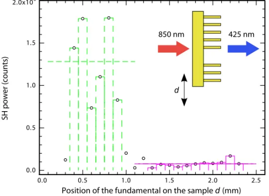
Figure 2.8 shows the SH signal at a wavelength of 425 nm as a function of the position of the fundamental beam on the sample (black dots), measured in transmission for sample B9138 with a 15% volume fraction of nanowires. The fundamental beam at a wavelength of 850 nm enters the sample at normal incidence from the substrate side (see inset) generating second harmonic as it propagates. Since the absorption length at a wavelength of 425 nm is only ∼ 200 nm for bulk GaP, we can assume that the SH signal in transmission is due to a thin layer (< 1µm) of the side of the sample facing the detector.
0.0 0.5 1.0 1.5 2.0 2.5
Position of the fundamental on the sample d (mm)
0.0 0.5 1.0 1.5
2.0x10⁶
SH power (counts)
d
850 nm 425 nm
2.5 Conclusion
Therefore, for the fundamental beam exiting the sample through the nanowire layer, the SH signal should have a large component due to the nanowires. By translating the sample relative to the fundamental beam we probe regions with and without the nanowires, without changing the angle of incidence on the sample.
In the experiment, the setup from Fig. 2.4(a) is slightly modified. A Ti:Sapphire laser is used to generate pulses at 850 nm with a duration of ∼2 ps full width at half maximum at a repetition rate of 80 MHz. The fun-damental is focused to a spot of ∼ 30 µm by a lens with a focal length of 100 mm. Since the nanowire layer acts as a highly scattering medium for radi-ation at 425 nm [36], a lens with a high NA of 0.5 and a focal length of 8 mm is used to collect the SH signal in transmission. The collimated second harmonic is focused onto a Peltier cooled CCD. A combination of the Newport band-pass filter FSR-BG39, with a transmission region of≈ 350–600 nm, and the Thorlabs shortpass filter FES0550, with a cut-on wavelength of about 550 nm, is inserted before the CCD to filter out the fundamental beam, and ensure the detection of the second harmonic signal only.
The dashed and solid bars in Figure 2.8 correspond to the SH signal origi-nating from the region without and with nanowires, respectively. The average second harmonic signal generated in the region without nanowires (horizontal dashed line) is ≈ 17 times larger than the average second harmonic signal generated in the region with nanowires (horizontal solid line). Apparently, nanowires on the sample do not lead to enhanced second harmonic genera-tion in the forward direcgenera-tion. We speculate that the main contribugenera-tion of the nanowires is to scatter the second harmonic generated in bulk GaP to angles inside the high refractive index substrate. This scattered second harmonic signal is not collected by our setup. Unfortunately, the current experimental data do not distinguish between scattered light and light generated by the nanowires, preventing a more detailed quantitative analysis.
2.5
Conclusion
The coherence length for second harmonic generation in bulk GaP at a wave-length of 1535 nm is more than two times larger then the wire wave-length of short GaP nanowires with a length of ≈ 1.3 µm. As a result, the contribution to the SH signal originating from the substrate is likely to be larger than the contribution originating from the nanowire layer.
2. Second harmonic generation in gallium phosphide nanowires
Chapter 3
Second harmonic generation in
freestanding AlGaAs photonic
crystal slabs
3.1
Introduction
Ever since the introduction as materials that can inhibit spontaneous emis-sion [5] or localize light [6], photonic crystals have been recognized as struc-tures that are able to tailor the propagation of light [9, 10]. These photonic crystals consist of a dielectric material arranged on a periodic lattice with a lattice constant comparable to the wavelength of light. Nowadays, photonic crystals find application in high Q, small mode volume cavities, in slow-light waveguides and numerous other applications that make use of the intriguing linear optical properties of photonic crystals. The nonlinear optics of photonic crystals, in particular second harmonic generation (SHG) is less intensively re-searched. Nevertheless, photonic crystals are interesting for nonlinear optics since they may combine high field intensities with optical properties that can be tuned by structure design.
phase-3. Second harmonic generation in freestanding AlGaAs photonic crystal slabs
matching is not easily satisfied. Phase matching can be satisfied in a device with periodically alternating layers of low and high index of refraction or by periodically poling the orientation of the χ(2) material. An existing phase mismatch can be compensated by adding or subtracting a suitable reciprocal lattice vector G resulting in what is called quasi-phase-matching [33, 43–45]. Second harmonic generation can be further enhanced significantly by a strong spatial confinement of both the fundamental and the SH optical fields [46], that enhances the field intensities. Two-dimensional (2D) photonic crystal slabs, i.e., slabs of dielectric GaAs material perforated with a lattice of holes, are interesting in this respect.
Cowan et al. [47] show theoretically how to exploit the leaky modes of a freestanding 2D photonic crystal slab to achieve both quasi-phase-matching and strong spatial confinement. The authors predict an enhancement of SH signal in reflection of more than 6 orders of magnitude.
Mondia et al. [48] investigate experimentally SHG in reflection from a 2D square lattice of holes in GaAs supported on an Al2O3 cladding layer. The authors use very short (150 fs) pulses and vary the angle of incidence and the frequency of the fundamental beam. This enables them to make both the fundamental and the SH wave resonant with the leaky modes of the structure. In this quasi-phase-matched configuration they achieve a SH enhancement of more than 1200 times compared to the noise level in the experiment. Torres et al. [49] present a theoretical and experimental study of SHG in reflection from a 1D GaN photonic crystal. They report a SH enhancement of more than 5000 times, compared to an unpatterned GaN slab, when the quasi-phase-matching condition is satisfied.
3.2 Fabrication of photonic crystals
reported in References [48,49]. We measure our largest enhancement when the fundamental beam is slightly off-resonance. This shows the importance of the resonant coupling occurring at the SH frequency (quasi-phase-matching) and hints at the fact that the enhancement may be much larger in a structure that is doubly resonant.
3.2
Fabrication of photonic crystals
The photonic crystal samples, investigated in this chapter, consist of a free-standing slab perforated with a two-dimensional square lattice of holes. The starting point of the fabrication process, similar to that of Ref. [50], is the heterostructure shown in Fig. 3.1(a), grown along the <100> lattice direction of the GaAs crystal [51]. The purpose of the fabrication procedure is to create a large, freestanding slab made out of Al0.35Ga0.65As perforated by a regular array of holes. A cross-section of this structure is shown in Fig. 3.1(b). The composition of the slab layer is chosen to render the structure optically trans-parent at both the fundamental (1535 nm) and second harmonic wavelength (767.5 nm).
The fabrication procedure starts with spin coating a∼500 nm thick layer of a positive-tone e-beam resist, ZEP 520A [52], on top of the heterostructure. The two-dimensional square lattice of holes is defined in the resist using e-beam lithography. To ensure a nonzero efficiency for second harmonic generation, the ΓX direction of the photonic lattice is rotated relative to the crystallo-graphic <100> direction of the underlying GaAs by an angle of ∼22.5◦. In this case, the incident electric field of the fundamental is never along a crys-tallographic axis of the GaAs wafer and the effective nonlinearity is nonzero. Collinear second harmonic generation along one of the crystallographic direc-tions is forbidden due to the 4¯3m symmetry of the GaAs lattice.
After e-beam exposure, the exposed resist is removed by developing for 80 sec. in n-amyl acetate and rinsing for 30 sec. in 9:1 methyl isobutyl ke-tone:isopropyl alcohol solution. The developed resist then serves as an etch mask for transferring the pattern to the silicon nitride (SiNx) layer using
anisotropic reactive ion etching (RIE) in a CHF3/Ar plasma. In this pro-cess a RF power of 50 W, a pressure of∼6µbar and CHF3 and Ar flow rates of 25 sccm are used. The etch rate of the SiNx layer is ∼15 nm/min and the
selectivity of the process is better then 10:1. After the pattern transfer, a low pressure RIE with an oxygen plasma is used to remove the residual e-beam resist.
3. Second harmonic generation in freestanding AlGaAs photonic crystal slabs
Figure 3.1. (a) Heterostructure used for fabrication of photonic crystal slabs. Photonic crystal slabs are made in the 150 nm thick Al0.35Ga0.65As layer. The silicon nitride layer provides the mask for
etching the hole pattern (defined by e-beam lithography) deep into the GaAs/AlxGa1−xAs layers. After removing the sacrificial layer a
standing structure is achieved. (b) Schematic cross-section of a free-standing photonic crystal slab with lattice constanta, radius of the holes
rand thicknessd.
into the GaAs/AlxGa1−xAs layers in a chlorine-based RIE etch [53]. The
flow rates of BCl3, Cl2, and N2 are set to 15, 7.5, and 10 sccm, respectively. A pure chlorine plasma leads to isotropic etching of the GaAs. This can be compensated by adding a sufficient amount of nitrogen to the plasma to passivate the sidewalls during the etching process. This way, near vertical etch profiles can be realized, ensuring straight holes in photonic crystal layer [54]. The RF power and pressure are 100W and ∼ 4.5 µbar respectively and the selectivity of the process is better than 10:1. Afterwards, the remaining silicon nitride mask is removed using the CHF3/Ar RIE as described earlier.
The 100 nm thick GaAs capping layer, on top of the structure, that protects the AlGaAs layers from oxidizing, is removed in a 3:1 citric acid:H2O2solution∗ etch for 2 minutes [55]. The GaAs layer is etched∼100 times faster then the underlying Al0.35Ga0.65As layer. In order to obtain reproducible results, any oxide layer residing on top of the capping layer should be removed prior to the etching process by dipping the structure in 15:1 deionized H2O:buffered oxide etch (BHF) solution for 15 seconds. Figure 3.2 shows a structure for which the removal of the GaAs is incomplete. The etching process is faster along the {100} crystallographic planes resulting in a square feature around every hole. From this image, the intentional∼ 22.5◦ misalignment of the photonic and the crystal lattice of GaAs is clearly visible.
After removing the sacrificial Al0.7Ga0.3As layer in a 1:4 HF (40%):H2O
∗
3.2 Fabrication of photonic crystals
solution for 1 minute [50], critical point drying is used to remove the sample from the liquid, resulting in a freestanding photonic crystal slab. The samples for this chapter were fabricated using the facilities of the Kavli Nanolab Delft. In this chapter, we investigate four freestanding photonic crystal slabs with the same lattice constant, but with a slightly different radius-to-pitch ratior/a
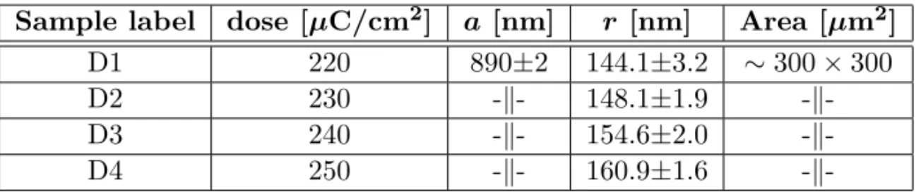
of the holes. These samples were created by writing the same pattern with e-beam using different exposures. Figure 3.3 shows an SEM image of sample D4 that was exposed with an electron dose of 250µC/cm2. From this image we find that the lattice constanta= 890±2 nm. An analysis of∼1000 holes shows
2s 2 1
(a) m (b) m
Figure 3.2. (a) and (b) SEM images of a photonic crystal sample with partially removed GaAs capping layer. Square feature around every hole arises from the fact that GaAs etches preferentially along the {100} crystallographic planes. The photonic lattice is rotated with respect to the crystal lattice of GaAs.
Figure 3.3. (a) and (b) Scanning electron micrographs showing the top view of freestanding photonic crystal slab D4. The entire structure covers an area of∼300×300µm2. The radius of the holes is 160.9 nm,
3. Second harmonic generation in freestanding AlGaAs photonic crystal slabs
that the radius of the holes is a normal distribution with an average radius of 160.9 nm and a standard deviationσ = 1.6 nm. The relevant parameters of photonic crystals D1–D4 are summarized in Table 3.1. As can be seen from the table, the hole size increases with electron dose. Varying the e-beam dose is a good way to fine tune ther/a ratio of a photonic crystal [56]. Samples D2, D3, and D4 have a similar distribution of hole sizes (equal σ) while D1 shows significantly more variation in hole size.
Table 3.1. Parameters of the photonic crystal slabs used in our exper-iments.
Sample label dose [µC/cm2] a [nm] r [nm] Area [µm2]
D1 220 890±2 144.1±3.2 ∼300×300
D2 230 -k- 148.1±1.9
-k-D3 240 -k- 154.6±2.0
-k-D4 250 -k- 160.9±1.6
-k-3.3
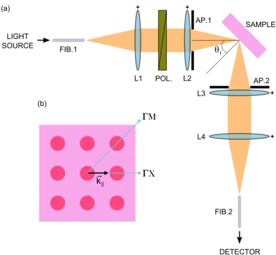
Setup
The experimental setup used for both linear reflectivity and second harmonic generation is shown schematically in Fig. 3.4(a). All the measurements are done in a specular geometry where the angle of incidenceθi is set by using a
motorized stage.
3.3.1 Linear reflectivity
3.3 Setup
FIB.1 LIGHT
SOURCE
DETECTOR L2
POL.
SAMPLE AP.1
AP.2 L3
L4
FIB.2 (a)
L1
X M
(b)
k||
i
Figure 3.4. (a) Setup used for both linear reflectivity and second har-monic generation. Light from an illumination source is coupled into a fiber (FIB.1) and focused on the photonic crystal sample at an angle of incidenceθi. The reflected light is collected into a second fiber (FIB.2)
and sent to a detector. The lenses L1–L4 serve to collimate and focus the light onto the sample. A polarizer (POL.) adjusts the polarization of the incident light. The apertures AP.1 and AP.2 can be used to reduce the numerical aperture of the incident and collected beams. (b) Schematic top view of a square lattice photonic crystal slab. Relevant symmetry directions are indicated as well as the parallel component of the wave vectork||.
by lens L3 (focal length of 75 mm), and focused by lens L4 (focal length of 50 mm) onto a 400 µm multimode fiber (FIB.2) and then sent to a fiber-coupled grating spectrometer.
3. Second harmonic generation in freestanding AlGaAs photonic crystal slabs
NIR-512 spectrometer (resolution≈ 3nm) is used for the infrared part of the spectrum (λ∼900–1700 nm).
3.3.2 Second harmonic generation
For SHG we slightly modify the setup shown in Figure 3.4(a). A Q-switched diode-pumped solid state laser (Cobolt Tango), with Er:Yb-doped glass as gain medium, is now used as the source of illumination. This laser has a specified center wavelength of 1535±1 nm and a narrow linewidth, <0.04 nm. The laser has a 5 kHz repetition rate with a typical pulse duration of≈3.8 ns (full width at half maximum). The average power of the laser is∼25 mW and high peak power pulses (∼1.3 kW) are generated. Light from the laser is coupled into a 9.5µm single-mode fiber instead of the 50µm multimode fiber used for linear reflectivity measurements.
The second harmonic generated in reflection is detected with either Ocean Optics USB4000 spectrometer (resolution ≈ 1.3 nm) or an Apogee Alta U1 Peltier cooled CCD camera. The CCD camera is used to detect very low second harmonic signals since it has much higher sensitivity compared to the fiber-coupled spectrometers.
3.4
Linear optical characteristics
The optical modes of a two-dimensional photonic crystal slab can be classified as truly guided modes and leaky modes (or guided resonances) [57]. Truly guided modes are the modes guided in the slab by total internal reflection. For these modes, all diffraction orders from the photonic crystal lattice are confined to the guiding layer as well. As a result, these modes remain confined to the slab and decay exponentially outside the slab. Leaky modes are the modes guided in the slab by total internal reflection that can couple to the environment via diffraction. In this case, at least one diffraction order from the photonic crystal lattice can propagate in the surrounding medium. Therefore, leaky modes can escape the slab and couple to the external radiation.
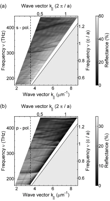
An effective way to investigate the leaky modes and their dispersion re-lation is to measure specular reflection spectra as a function of angle of inci-dence [58, 59]. Each guided resonance will appear as a resonant feature in the reflection spectrum on top of a slowly oscillating background [60]. Figure 3.5 shows a plot of the measured reflection for sample D4 as a function of fre-quency on the vertical axis and the in-plane wave vectork|| on the horizontal
3.4 Linear optical characteristics
(a)
(b)
Figure 3.5. Gray scale plot of the measured reflection as a function of frequency (vertical axis) and wave vectork|| (horizontal axis) for sample
3. Second harmonic generation in freestanding AlGaAs photonic crystal slabs
steps of 1◦. In order to facilitate a comparison with a dispersion relationν(k||),
the angles of incidence are converted to the in-plane wave vectors using the expression k|| = (2πν/c) sinθi, where θi are the angles of incidence, as shown
in Figure 3.4(a). The sample is oriented in such a way that the in-plane wave vector,k||, is along the ΓX symmetry direction of the photonic crystal lattice.
The incident light beam is focused to a spot of ∼75 µm with a numerical aperture∼0.025. Several sharp resonant features can be observed in the fig-ure indicating the dispersion of leaky modes. The gray shaded area below the light line (ν=ck||/(2π)) is the region of the truly guided modes.
In order to understand the position of the leaky modes, we calculated the band structure of the leaky modes using a freely available finite difference time domain (FDTD) package∗. In the calculation, the slab has a radius of the holes
r/a= 0.18, a thicknessd/a = 0.13, and a relative permittivity= 10. These parameters correspond to those of sample D4. For simplicity, we assume that the photonic crystal material is lossless and dispersionless and use a literature value [62] of the permittivity of Al0.35Ga0.65As at a wavelength of 1500 nm. It is well-known that below the electronic band gap, the permittivity increases with frequency. Therefore, we expect that the calculated modes are slightly blue-shifted for larger frequencies compared to a calculation that takes into account dispersion. This is a relatively small effect in the frequency range where we compare the calculated band structure with measured data.
Figure 3.6 shows the calculated band structure of leaky modes plotted on top of the experimental reflectivity data for sample D4. We restrict ourselves to frequencies ν below 300 THz for clarity. Calculations are shown for both H-even (TE-like) and E-odd (TM-like) modes.
In the calculation, the 2D square lattice is positioned in thexy-plane and a point dipole source is placed in the middle of the photonic crystal slab atz= 0. The modes of a photonic crystal slab can be classified by their E-field, which is either even or odd with respect to the mirror-symmetry plane at z = 0. Even modes have the H-field in the z-direction, while odd modes have the E-field in thez-direction. In the case of an unpatterned waveguide slab, these modes correspond to the fundamental transverse electric (TE) and transverse magnetic (TM) modes. Note however, that this definition of TE and TM is relative to a plane of continuous translational symmetry, perpendicular to the slab; e.g., thex = 0 plane. This continuous translational symmetry is broken in a 2D photonic crystal slab and the optical modes cannot be labeled as TE and TM modes [63]. We will refer to these modes as a TE- and TM-like mode
∗
3.4 Linear optical characteristics
(a)
(b)
3. Second harmonic generation in freestanding AlGaAs photonic crystal slabs
to emphasize the resemblance of these modes to those of an unpatterned slab. As can be seen, the calculated and the experimental data are in good agreement. From the figure we conclude that there is no coupling to TM-like leaky modes in this frequency range while a number of TE-like leaky modes are visible in the experimental data for both s- and p-polarized incoming light. External radiation couples to the guided resonances of the photonic crystal via diffraction by adding a reciprocal lattice vector G to the in-plane wave vector k||. We define the wave vector of the incident light in the xz-plane,
with the x-axis parallel to the ΓX direction of the photonic lattice. Each leaky mode can be labeled by the reciprocal lattice vector (Gx, Gy) involved
in the coupling of the incoming light to the leaky mode.
In order to understand the coupling of the incident light to a leaky mode one needs to understand the symmetry of these modes in the plane of incidence. In our case, the plane of incidence is thex = 0 plane of mirror symmetry of the photonic crystal. The E-field of the leaky modes is either odd or even relative to this plane. Note that this definition of odd or even is an additional symmetry in addition to the mirror symmetry of the z = 0 plane discussed before. The E-field of the incoming s- or p-polarized light is either odd or even relative to the x = 0 plane. This determines the coupling of light to the slab modes.
Let us first consider the coupling to (±1, 0) and (0, ±1) modes. At non-normal incidence all degeneracy of these modes is lifted. The (-1, 0) and (+1, 0) modes show strong dispersion and propagate in the direction of the incoming wave vector. These TE-like modes are odd with respect to thex= 0 plane and couple to s-polarized light. The (0,±1) modes propagate in and out of plane direction, and as a consequence have a weaker dispersion. The lower energy (0,±1) mode is a superposition of a (0, +1) and (0, -1) mode with odd symmetry relative to thex = 0 plane and couples to s-polarization. The high energy (0,±1) mode is even and couples to p-polarization [64]. This is indeed what is observed in Fig. 3.6. In the experimental data for s-polarization (Fig. 3.6(a)), going from low to high frequencies, we see a lower energy (0,±1) mode, a (-1,±1) mode, a crossing of (1, 0) and (-2, 0) modes, and a crossing of (1,±1) and (-2, ±1) modes. The (-1, 0) mode is too low in frequency to be observed in the experiment. In p-polarization (Fig. 3.6(b)), we see a higher energy (0,±1) mode, a (-1,±1) mode with low Q (not resolved with MEEP calculation∗), and a crossing of (1,±1) and (-2, ±1) modes.
Sample D4 was designed in such a way to enable the coupling of a
s-∗
3.4 Linear optical characteristics
polarized fundamental beam at frequency νF = 195.44 THz to one of the
first leaky modes. From Figure 3.6(a), it is evident that the fundamental can resonantly couple to the structure by exciting the lower energy (0, ±1) mode. In order to determine for which value of the in-plane wave vector k||
this is achieved we have to extract the dispersion of this leaky mode from the experimental reflectivity data.
Figure 3.7 shows reflection spectra of sample D4 for s-polarized incident light and various values of k||. Each reflection spectrum contains sharp
res-onant features superimposed on top of a smooth background. The asym-metry of the (Fano) resonances is a result of an interference between a di-rect (non-resonant) and indidi-rect (resonant) channel, as was first described by Fano [65, 66]. Light in the non-resonant channel is Fresnel reflected from the slab, while light in the resonant channel couples to a leaky mode of the struc-ture and after some time “leaks” back into the environment. Fan et al. [60]
190 195 200 205 210
30 60 90 120
Reflectance (%)
Frequency ν (THz)
k||= 2.632 µm−1
νlaser s−polarization
k||= 2.896 µm−1
νlaser s−polarization
k||= 3.137 µm−1
νlaser s−polarization
k||= 3.355 µm−1
νlaser s−polarization
k||= 3.547 µm−1
νlaser s−polarization
k
||= 3.712 µm −1
νlaser s−polarization
Figure 3.7. Experimental reflection spectra of sample D4 (blue curves) for s-polarized incident light and different values of k||. Measured
3. Second harmonic generation in freestanding AlGaAs photonic crystal slabs
have developed a general temporal coupled-mode theory of the Fano resonance for a single-mode optical resonator coupled with multiple input/output ports. A photonic crystal slab can be treated as a single-mode optical resonator with two ports, one at each side of the structure. Light, can be transported from one port to the other using both a non-resonant and a resonant channel. The resonant channel is characterized by a frequency ν0 and a time τ. We define the escape rate of a resonance as Γ = 1/(2πτ) and the quality factor of a reso-nance asQ=ν0/(2Γ). For a symmetric two port system, e.g., a freestanding photonic crystal slab in air, the reflectance R as a function of frequency ν is given by R=
rD+ Γ
−rD∓itD i(ν−ν0) + Γ
2 , (3.1)
whererD andtD are the Fresnel reflection and transmission coefficients of the
slab. The subscript “D” is used to denote the direct channel. The ∓ sign is due to exciting eithereven(-) orodd(+) leaky mode with respect to the plane of mirror-symmetry going through the middle of the slab (z = 0).
For a lossless system, the asymmetric Fano lineshape given by equation (3.1) reaches both 0% and 100%. In realistic systems, losses are present. These losses are either due to the absorption of the slab material or scattering from imperfections of the structure. Driessen et al. [67] have extended the coupled-mode theory of the Fano resonance by adding an extra port to include losses in the system. It is assumed that energy in the photonic crystal resonator is transferred irreversibly to the loss port and is characterized by a loss rate
γ. The resonant Fano features in the experimental data, for a freestanding photonic crystal slab in air, can be described using the following expression for the reflectanceR:
R=
rD
+ Γ −rD∓itD
i(ν−ν0) + Γ +γ 2 . (3.2)
In order to fit the measured Fano resonances corresponding to the lower energy (0,±1) leaky mode (Fig. 3.7), the expression (3.2) is rewritten in the following form: R= c1
+c2ν−
c3+ic4
i(ν−ν0) +γ+ Γ 2 , (3.3)
3.4 Linear optical characteristics
(ν0as a function ofk||) and the quality factor (Q=ν0/(2(Γ +γ)) as a function ofk||) of a leaky mode directly from the experimental data. Figure 3.8 shows
the dispersion of the lower energy (0,±1) leaky mode of sample D4 (blue dots). The frequency of the fundamental is indicated by the red dashed line in the figure. The green dash-dot line defines a constant angle of incidenceθi = 46◦.
From this figure it is clear that the s-polarized fundamental beam couples resonantly to a leaky mode at an angle of incidenceθi = 46◦, corresponding
tok|| = 0.417×2π/a. A typical quality factor Q=ν0/(2(Γ +γ)) of this leaky mode, as determined by the Fano model, is∼175.
0.2 0.3 0.4 0.5
0.55 0.57 0.59 0.61
θi=46°
νlaser
s−pol. p−pol.
Wave vector k
||
(2
π
/ a)
Frequency
ν
o(c / a)
1.3 1.8 2.3 2.8 3.3 3.8
190 195 200 205
Frequency
ν
0(THz)
Wave vector k
||
(
µ
m
−1)
Figure 3.8. Measured dispersion of the lower energy (0,±1) leaky mode of sample D4 (blue dots). The red dashed line indicates the position of the fundamental frequency, and the green dash-dot line corresponds to a constant angle of incidence θi = 46◦. Resonant coupling of the
s-polarized fundamental beam to the (0,±1) leaky mode occurs at an angle of incidenceθi= 46◦. A simple analytical model, based on a nearly