Master Interface For On-Chip Hardware Accelerator Burst
Communications
Antoine Fraboulet
Compsys, Lip
46 All´
ee d’Italie
69363 Lyon cedex 07
France
[email protected]Tanguy Risset
Citi, Insa-Lyon,
21 av. Jean Capelle
69621 Villeurbanne Cedex
France
Abstract
We explain a systematic way of interfacing data-flow hardware accelerators (IP) for their inte-gration in a system on chip. We abstract the communication behaviour of the data flow IP so as to provide basis for an interface generator. Then we measure the throughput obtained for different architectures of the interface mechanism by a cycle accurate bit accurate simulation of a SoC inte-grating a data-flow IP. We show in which configuration the optimal communication scheme can be reached.
Keywords: system on chip, SoC simulation, high level synthesis, interface generation
1. Introduction
Large scale systems on chip (SoC) design is faced with many problems among which efficient communication managing is one of the most important. In the past, communication efficiency has already been one of the major burden in parallel machine development but in addition, today’s on-chip communications are limited by the power consumption problem. Network on chip based SoC architectures are not arriving as fast as envisaged because of the power consumption problem. In addition, shorter design time is required to meet the ever increasing time-to-market constraints. IP re-use and platform based design are pointed out as solution to faster design but they are still confronted with important limitations and are not really used in today’s industrial design flows. Examples of these problems are: IP standardisation, system on chip cycle accurate simulation time [22, 21], and fast integration of special purpose hardware in a design environment.
We address the problem of providing a rapid and efficient integration of a special purpose hard-ware accelerator into a complex system on chip possibly integrating many processor cores and important software applications. More precisely, we will focus on the category ofstream process-inghardware accelerators. Stream processing performs on-the-fly costly computations on streams of data. The amount of control in these computations is reduced, but the complexity lies in the quantity of computations usually submitted to soft real time constraints (as for audio or video processing). Hardware accelerators containing parallel computation usually presented in the form of arrays of processors are mandatory to meet these constraints. we refer to these accelerators as
data-flowips. Systolic arrays are examples of such data-flow ips but they are not the only ones. In this paper we only target linear array of processor which have a small number of input/output ports, the problem of interfacing 2D array of processors has been studied in [7], but the problems
encountered are quite different and many ipintegrated to SoC are 1D arrays because of the high bandwidth required by 2D arrays.
The hardware accelerators used in SoC for portable communication systems (cell-phones,pda,. . . ) are originally designed by hardware designers in collaboration with signal processing engineers. For theseips, the performance bottleneck lies in the communication of the data between memory and theip. The paradigm used for specifying and designing these circuits is called thedata-flowmodel: designers manipulates streams of data which input and output the circuits without any information about the external storage of these data. The interface protocol isdata synchronisedwhich means that the behaviour is regulated by the consumption and production of data at the boundaries of the architecture. In this protocol, if the data is not present the computations are stopped, usually with a clock enable mechanism.
Until recently, theseips where designed by hand with a precise methodology, knowing in advance the target SoC architecture. Hence the design of the interface was more or less performed together with the architecture. New trends in SoC design require the use of tools to accelerate the design phase of specific hardware accelerators. These tools are calledhigh level design,behavioural synthesis
tools orhardware compilers [11, 5, 24]. Most of the time, because of the huge design space they propose to the user a toolbox for tuning parameters of the resulting architecture. However, even if these tools greatly accelerate and secure the design of the ip itself, the time needed to write the interface may render the tool simply useless. Today, these tools produce some configuration information that helps in the design of the interface, but this part has not been standardised. In this paper, based on the experience of MMAlpha [8, 10] and Gaut [5], we identify the common concepts that are used by data-flow ip designers to propose a generic interface mechanism. This generic interface mechanism will be parameterised by the configuration information output from data-flow ip generators. We also hope to bring a standard way of describing data-flow ip input/output behaviour so as to facilitateipreuse.
We introduce in this paper some theoretical foundations for the automatic generation of data-flow ips interface. As a reference to data-flowmodel of computation used to buildips, we introduce the data flowmodel of interfacewhich basically rely on a data synchronised protocol. We highlight the various parameters that must be taken into account to adapt the data-flowipto various SoC platform and we validate this high level interface design concept by a complete cycle accurate SoC simulation using the SocLib simulation environment and a high level designed hardware accelerator synthesised with the MMAlpha tool [11]. We provide many experimental results concerning communication performances for various architecture of the interface. The major conclusion of this work is that optimal communication scheme can be reached only if the interface of the hardware accelerator is master, i.e. contains adma, and moreover thisdmahas to have a small degree of programmability: it must be able to execute repeatedly a small sequence of transfers.
2. Hardware/Software Interface Of Data-Flow IPs
In this section, we precisely identify the context of the work, it implies precise definition of what we call data-flow ip, the schematic architecture of the system on chip we target and the overall principles of the hardware/software interface that we wish to generate.
2.1. Data flow IP and SoC environment
In recent SoC design, many processors ips are to be connected on a communication medium which can be a bus, a hierarchical bus or a network. We will refer to this communication medium as thebuseven if this work can be applied to network on chip based SoC architectures. The processors are usually initiators, in the sense that they initiates communications. In addition, several other
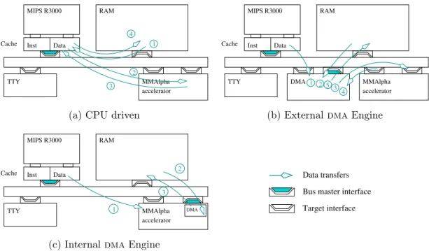
MMAlpha accelerator TTY MIPS R3000 Data Inst Cache RAM 3 2 1 4
(a) CPU driven
MMAlpha accelerator TTY MIPS R3000 Data Inst Cache RAM DMA 2 3 4 1 5
(b) External dmaEngine
TTY MIPS R3000 Data Inst Cache RAM MMAlpha accelerator DMA 2 3 1
(c) InternaldmaEngine
Bus master interface Target interface Data transfers
Figure 1. The three main interface modes: (a) CPU driven, (b) external
dma
and (c)
internal
dma
engine
ips are connected on the bus: memory, hardware accelerators, external communication systems, bridge to other buses and so on. In most recent SoC architectures the only hardware to be designed specifically will be some hardware accelerator dedicated to a particular algorithm to be executed on the SoC.
From the external communications point of view, a data flowipis a black box controlled by data arrival which receives and sends data possibly at each clock cycle. It has a number of input ports and output ports each of which having a certain bit-width. We assume that, in addition to the clock, theiphas aclock enablepin that can freeze the execution of theip. Hence, if the clock enable is not set, everything behave in theipas if the clock was not changing. This allow us to define the notion ofvirtual clock, the virtual clock is the one seen inside the ip, it does not take into account the clock changes that are not validated by the clock enable. Then, we assume that theipis data synchronised, i.e. at each clock cycle, data are presented on the input port and at the raise of the clock (provided that the clock enable is set), the data is read by the ip. If all the required data are present and the clock enable is set then theipcan run for a cycle which increments the virtual clock counter. We do not assume that there is a hand shake protocol at this level of abstraction. In practice there is a hand shake protocol at a lower level, but it can be abstracted thanks to the virtual clock mechanism.
The target SoC platform is represented on Fig. 1, ips are connected to the bus via the vci interface protocole. vci[1] is a low level point to point protocol standardised by the vsiAlliance and permits to interconnectips independently of the protocol used by the bus. A mipsprocessor executes a stream-processing like application and uses a hardware ipto accelerate computations. Theiphas been generated withmmalpha high level synthesis tool [11], hence it is namedMMAlpha acceleratorin Fig. 1.
2.2. Hardware/Software Interface Global Scheme
In general we assume that the hardware accelerator will be controlled by a processor (that we call thehostprocessor). Hence the interface of theipis composed of a software part and a hardware
part. The software part will command the data communication between memory and the ip, we call this part thedriver. From our experience [8, 10], the communication scheme used to feed the hardware accelerator must respect important constraints so as to obtain acceptable performances: (i) it should try to use a Direct Memory Access module (dma) to perform communication in burst mode, but only when it increases performances; (ii) the designer can set the burst size to balance between hardware cost, communication latency and bus contention. Also, the architecture of the hardware/software interface must be re-usable for many different data-flowip. It can be envisaged in three main modes depicted in Fig. 1: either the driver on the host processor directly executes all the communications or it simply controls a dmawhich himself performs the communications between the memory and theip. The use of this dmacan be made much more efficient if thedma is designed specifically to this generic interface control mechanism and is directly connected to the ip as shown on 1-c and demonstrated in section 4. The proposed interface mechanism must be used in various SoC architectures, hence we think that aninterface generatortool must be used to generate various versions of the interface depending on targeted SoC parameters, this is detailed in next section.
3. Generic Interface Generation Principles
In this section we identify the concept that are useful to build an interface generator for data-flow ips.
3.1. Communication Activity Abstraction
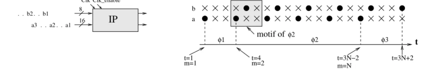
The crucial point is to abstract theipcommunication activity in such a way that it is (i) platform independent and (ii) compact. To be platform independent, one has to identify the communication activity that depends only of theip. To be compact one must use loop like formalism to express a large number of communication in a very small space. The use of parameters not known at compile time in these loop is mandatory. The theoretical background of our work is based on the polyhedral model which uses polyhedra to abstract loop iteration domains. However, interface synthesis for linear arrays does not need a important knowledge on polyhedra as the only polyhedra manipulated are 1-dimensional. . . b2 . . b1 8 16 Clk Clk_enable
IP
a1 . . a2 . . a3 t b a t=1 t=4 t=3N−2 t=3N+2 φ1 motif of φ2 φ2 φ3 m=1 m=2 m=NFigure 2. Graphical representation of input/output on a simple data-flow IP
Consider a very simple example: a hardware module that processes two streams a1,a2,. . . and
b1,b2,. . . (only the input interface is detailed here). The a stream is 16 bits wide while the b
stream is 8 bits wide. Thisipinputs the firstasample att= 1 and then oneasample every three clock cycle untilN samples have been processed. The t counter corresponds to a counter on the virtual clock of theiphence we are currently observing the behaviour frominsidethe module, it is initialised with the reset of theip. Thebstream is input at the same rate (one sample every 3 clock cycles) but starts att= 5. Theipis represented on the left of Fig. 2, many signal processing filters have the same kind of input/output behaviour: each stream is composed of a sequence ofsamples
arriving at a regular rate. The schedule of the inputs can be graphically represented by the right of Fig. 2, forN = 6.
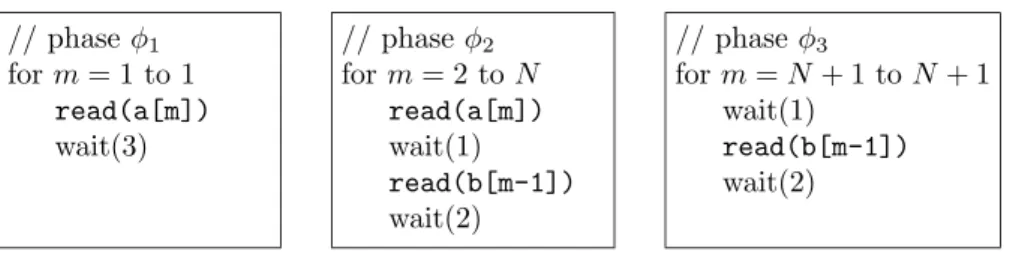
// phaseφ1 form= 1 to 1 read(a[m]) wait(3) // phaseφ2 form= 2 toN read(a[m]) wait(1) read(b[m-1]) wait(2) // phaseφ3 form=N+ 1 toN+ 1 wait(1) read(b[m-1]) wait(2)
Figure 3. Data flow interface format used for specifying input/output behaviour of
the IP of Fig. 2
The input interface behaviour has threephases. During the first phase, only ais input, then a
andbare input, and finally there is a phase where onlybis input. Because of the stream processing behaviour of the application, we can divide each of these phases into the repetitive execution of a motif which corresponds to the consumption of one sample of each stream (right of Fig. 2). We define a motif as a small sequence of steps (here 3 steps) where I/O performed by each port are precisely defined. Here, each sample of streamais input every 3 clock cycles. Hence, the I/O behaviour on portacan be described as a repetitive execution of a simple motif: one step with input and two steps without input. The motif of streambhas the same length, hence the I/O behaviour during phaseφ2 can be expressed asN −1 execution of a simple motif which is illustrated on the
right of Fig. 2. In general the length of the motif of a phase is the least common multiple of the length of the motifs of all the streams involved.
To specify functional behaviour of theip, the motif indexmcan be used rather than the virtual clockt. Of course, as we are in the data flow model, there will always be a relation between the motif indexm and the virtual clock countert. For our example, this relation can be expressed as: in phaseφ2the motifmstart its execution att= 3m−2, this relation can be easily established once
the motif has been defined. In addition we need a way to identify which data is concerned with a particular motifm. For that we assume that data input on a particular port are successive elements of a linear array. Any other indexing is possible, however, it should be as close as possible as the memory layout of the corresponding variable in a target SoC.
We gather the phase and motif information into the data-flow interface format presented in Fig. 3 which permits to represent the input behaviour of the architecture of Fig. 2 without assigning a value to N. In these loops, the m index is the motif index or equivalently the number of the sample treated. The virtual clock countert can be reconstructed using thewaitinstructions. The instructions have a 0 cycle execution time except thewait()statement whose execution time is the argument. The phases and motifs completely define the communication behaviour of the ip. Any ipwhose input/output behaviour cannot be expressed with these concepts cannot be interfaced by our mechanism. Note that it strictly implies data-independent communications, the communication scheme must be statically defined before the computation starts.
This data-flow interface format should be parsed by the interface generator. During this process, the polyhedral model can be used to store the internal representation of the phase and motif infor-mation. For instance, the virtual clock cycles at which theipshould read on portaare the integers of the following set: { 3m−2 | 2 ≤m≤ N }. This set is called a Z-polyhedron. Researches on the polyhedral model [23] have shown how to store and manipulate these sets without knowing the value ofN. Building this set during the parsing of the data-flow interface program of Fig. 3 is easy. The scheme of the interface mechanism is depicted in Fig. 4, it will be explained in next section. Just note that FIFOs are placed between the bus and theIPto buffer the data. In order to integrate theip into a SoC, we need some more information, in particular the size of the bus and the size available for the FIFOs used to buffer data before theip. we define the communication scheme by a succession ofcommunication patterninside each phase: acommunication patternis the set of data that will be sent to the architecture to feed the architecture during a particular phase. A pattern can gather several motifs in order to take advantage of the bus burst mode. Input pattern and output
pattern must be carefully merged taking into account buffering available to avoid deadlocks. On our example, during phaseφ2, if we have FIFOs containing 20 data ofaandbbeforeipinput ports,
and assuming that the bus width is 32 bits, we can use the following pattern: send 10 bus-words of
a, then send 5 bus-words of datab(remember thatbhas a twice smaller bit width). To sum up the important concepts that we have introduced in this section:
• The input/output behaviour of theipis divided into a finite number ofphases. A phase is a period during which communication occurs only on (possibly many) fixed ports.
• A phase repeats from one to a very large number of time (possibly fixed at run time) amotif. A motif has a fixed number of virtual clock cycle. It describes the repeated behaviour of the input and output of the interface for each sample during a particular phase.
• A pattern(or communication pattern) is the set of data that will be sent to the architecture to feed the architecture during a particular phase.
3.2. Generic Interface Description
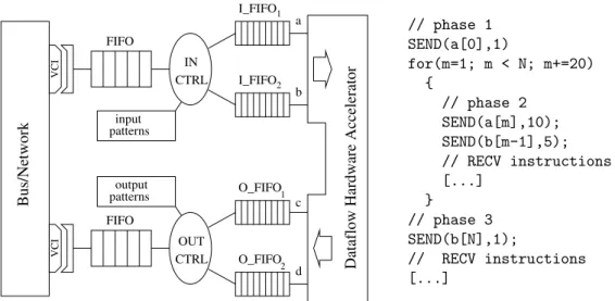
I_FIFO1 I_FIFO2 O_FIFO1 O_FIFO2 FIFO FIFO CTRL CTRL IN OUT input patterns patternsoutput VCI VCI
Dataflow Hardware Accelerator
a b c d Bus/Network // phase 1 SEND(a[0],1) for(m=1; m < N; m+=20) { // phase 2 SEND(a[m],10); SEND(b[m-1],5); // RECV instructions [...] } // phase 3 SEND(b[N],1); // RECV instructions [...]
Figure 4. Hardware and Software interfaces for the Data-flow hardware accelerator
of Fig. 3. Controllers must be configured according to communication patterns
used in the software driver on the right hand side.
We are now able to introduce the basic architecture of our interface mechanism. It is represented on Fig. 4 with a maximum burst size of 10 bus words. The hardware part is on the left. The proposed architecture has two target interfaces on the interconnect. These two ports can be reduced to one if simultaneous input and output are not feasible as it is the case when the interconnect is a bus. Data received from the host processor through the bus are de-multiplexed according to the communication pattern of the current phase. The hardware performing this control is a simple automaton parameterised by phases, motifs and communication patterns, we call it thecontroller. The software driver executed on the host processor is represented on the right. One can see how the patterns are used to write the driver (only input instructions are detailed). The compatibility between the controller configuration and the driver is essential, both should be generated by the same tool. This is the major argument for an interface generator.
The interface generator reads input/output behaviour of theipexpressed in a particular format such as the data-flow interface format presented in Fig. 3 and produces the corresponding hardware
controller and software driver. This generator should be able to include many parameters in addition to the ip parameters. For instance, the designer should be able to specify the maximum size of burst allowed, as well as the size of the FIFOs present in the interface generated. A good interface generator should be insensitive to a change of master processor, i.e. it should be easily retargeted to a new assembly langage or interruption handling strategy.
Finally the interface generator should be adaptable to different memory layout of the streams. The difficult part is to make the phase/motif information and the memory layout organisation compatible. In our version, we have assumed that successive data that enters a particular input port of the ip are stored contiguously in the memory. If this is not the case, as for instance for interleaved data in stereo signal processing, and if we still want to use burst access to memory, the interface must merge the memory layout organisation with the pattern information to program the controller. We think that this is very difficult to do in a generic way, hence we propose to generate a communication pattern mechanism interface for a fixed memory layout organisation of each stream, the most common case being the in-order data layout organisation.
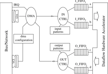
I_FIFO1 I_FIFO2 O_FIFO1 O_FIFO2 Bus/Network VCI input patterns patternsoutput configurationdma VCI CTRL CTRL IN OUT
Dataflow Hardware Accelerator
a b c d DMA IRQ
Figure 5. Hardware DMA interface implementation using a single data port for the
Data-flow hardware accelerator of Fig. 3.
4. Experiments: Cycle Accurate SoC Simulation
Performance results for this particular kind of experiments are very dependent on some target architecture characteristics as for instance the behaviour of the caches. It is now well known that cache behaviour and network congestion are very difficult to predict, hence the only way to validate our interface mechanism is to perform a cycle accurate simulation of the whole system. We have performed these simulations with the SocLib (http://soclib.lip6.fr/) environment and mea-sured the performances obtained with the three main interface modes presented in figure 1, we have also measured the impact of the burst size on the communication performances. The description of the experimental setting is performed in section 4.1, the results are analysed in section 4.2.
4.1. Target Platform And Design Methodology
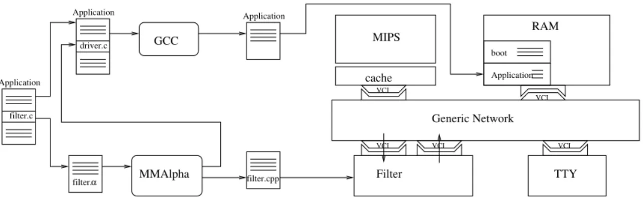
We have chosen to execute a classical audio signal processing application that processes stereo audio files and proposes various simple filters likelp’s tick removal. As we mentioned before, we are interested in non-interleaved streams. Writing an interleaved version of the interface would not be very difficult and would only require a modification of the input and output controllers used within the interface. We have added an 8 tapfirfilter, a simple convolution with 8 multiplication and 8 additions. We have provided a SystemC module implementing a data flow hardware accelerator for this filter. The target platform that we want to simulate is composed of a processor, a memory, the hardware accelerator connected on a communication medium (see right of Fig. 6).
Simulation of the SoC platform was done in SystemC using the SocLib environment. The main component of SocLib is currently a set of SystemC simulation models for commonips (mips pro-cessor,ram, NoC, busses, dma). All these simulation models use vciinterconnection standard [1]. These simulation models are publicly available and there exists synthesizablertlversions of theips that can be used for the final design. The hardware accelerator was synthesised withmmalpha [11]. mmalpha is a toolbox for designing regular parallel architectures (systolic like) from recurrence equation specifications expressed in the Alpha language. It is one of the only existing tools that really automates the refinement of a software specification downtortl description within the same language: Alpha. We have developed a translator from AlpHard (hardware description language, subset of Alpha) to SystemC [10]. We wrote by hand a SystemC version of the generic interface presented in this paper and we generated from mmalpha the configuration of the controller and the software driver for different parameters of the experiments (size of the burst, different types of interface) etc.
Providing a complete refinement methodology using high level synthesis from a bulk software specification is not easy, we explain here precisely what we did from the original C-code, it is illus-trated in Fig. 6. We have extracted from the C-code a function (referred asfilter.c) performing the filter, and translated it in Alpha by hand (filter.alpha). Driven by the user,mmalpha will refine this specification downto a hardware description specification in the Alpha language (referred as AlpHard format). At any step of the refinement,mmalpha can generate C-code for simulation. The filter manually translated in Alpha was validated by replacing the originalfilter.cfunction by the C code generated from thefilter.alphabymmalpha and testing resulting execution against original program. Then mmalpha generated a systolic version of the filter from which we gener-ated a SystemC simulation model (filter.cpp), and a SystemC file for configuring the hardware interface and the software driver (driver.c). The software driver replaced the originalfilter.c
in the program before its compilation to themipsprocessor. In the particular instance of the SoC represented in figure 6, there is no dma, this driver explicitly performed all the communications between the memory and the hardware accelerator as did the driver represented on the right of Fig. 4. Hence, on Fig. 6, the box labelled Filter is composed of the generic interface plus the SystemC files generated bymmalpha: interface configuration andfilter.cpp.
The hardware components of the platform are: amipsR3000 processor (with its associated data and instruction cache) also referred as thecpu, a standard memory, a component used for displaying output (referred astty) and the a specific hardware accelerator generated withmmalpha including the interface. All these components are connected via vci ports to a simple network (internal architecture of this network is not precisely simulated, only the latency and bandwidth can be parameterised). All these components are memory mapped, i.e. the mips has access to the input and output ports of the hardware accelerator as two particular memory locations. The software running on the mips, in addition to bootstrapping information, is composed of the C program cross-compiled withgccto amipstarget.
We have written three SoC platforms to simulate the three types of interface illustrated in Fig. 1. In the first platform (Fig. 1-a), thecpu drives all communications: in order to send a data to the accelerator, the software driver running on themipsmust read the data in the memory and write it
VCI VCI VCI filter.c Application Generic Network VCI VCI Filter TTY cache MIPS RAM MMAlpha GCC filter.α Application filter.cpp Application boot Application driver.c
Figure 6. The SoC simulated and the global design methodology. Square boxes
represent SystemC models of
ip
s.
at the memory location of the accelerator I/O ports, this is illustrated by arrows 1 and 2 on Fig. 1-a, this is also what performs theSEND macro of Fig. 4. In this version, the accelerator contains two slave ports: one for input, one for output.
The second platform uses an externaldma that can outperform thecpu by using longer com-munication burst on the interconnect, it is represented on Fig. 1-b. If thedmais parameterised to perform one burst, the behaviour of aSENDis the following: themipsconfigures the dma, then the dmareads the data in memory and writes it to the hardware accelerator (in burst mode, arrow 1, 2 and 3 of Fig. 1-b), then it raises an interruption to indicate to themipsthat the communication occurred. This interruption is a major problem because it takes approximately 380 cycles to be handled by the mips. In order to minimise the impact of the interruption, we have authorised the scatter-gather scheme for the dma: thedma can store more than one burst communication con-figuration, the number of configuration stored is a parameter of our experiment, this is a classical improvement ofdmaengines. We are promoting another modification of thedma: because of the very regular nature of our communications (transmitting continuous streams), the configuration of thedmais always the same up to the starting address of the data which is incremented regularly. If we could, for instance implement the loop present on the driver of Fig. 4insidethedma, we would gain a lot of interruption handling (N/20 in the example of Fig. 4). This can be easily done by providing an additional register in thedmawhich indicates how many times the configuration stored on thedmamust be executed before waking up thecpu. We have implemented this improvement in the simulation model of ourdma.
The third platform is simply obtained by putting thedmainsidethe hardware accelerator. This is a natural improvement, as shown in Fig. 5, it immediately divides the number of communications by two. In this version, the hardware accelerator contains one slave port for configuration by the mipsand one master port for initiating communications with the memory (Fig. 1-c).
4.2. Experimental Results
In this section we only measured the portion of code composed of the originalfilter.c. Some performance results are presented in table 1, in this table and in the rest of the section, the term cpu refers to the first platform (Fig 1-a), the term external dma refers to the second platform (Fig 1-b) and the the terminternal dmarefers to the third platform (Fig 1-c). This table shows an average simulation speed of 50 000 cycles per second, there is no major difference in simulation speed between the three platforms, the only difference is for the loop enabledmaplatform that is slightly slower due to the activity increase that has to be simulated. We can immediately see the improvement of the internalloop enabledmaplatform: a throughput of 254 000 samples for 600 000 cycles is obtained. The theoretical maximum throughput that can be obtained is 300 000 samples
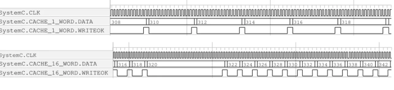
308 310 312 314 316 318 316 318 320 SystemC.CLK SystemC.CACHE_1_WORD.DATA 322 SystemC.CACHE_1_WORD.WRITEOK 324 326 328 330 332 334 336 338 340 342 SystemC.CLK SystemC.CACHE_16_WORD.DATA SystemC.CACHE_16_WORD.WRITEOK
Figure 7. Effect of different size of data cache lines (1 bus word and 16 bus word)
on the arrival of data to the
ip
.
for 600 000 cycles, indeed each sample is 16 bits wide, there are two sample stream which must be at least read once from the memory and write once to the memory, hence with a memory answering in one clock cycle and a bus width of 32 bits we cannot compute more than 300 000 samples for 600 000 cycles. The internal loop enable dmaversion is nearly optimal. There is no major difference between thecpu version and the dmaversion because the improvement provided by the burst of thedmais counter-balanced by the overhead of thedmainterruptions.
cpu ext. dma int. dma int. dmaw/ loop
complete simulation time (seconds) 10.91 12.82 10.91 18.26
complete simulation cycles 600000 600000 600000 600000
simulation speed (cycles/seconds) 54995.5 46802 54995.5 32858.8
hardware pipeline throughput (samples) 16861 10561 9601 254041
Table 1. Performances obtained from the complete SoC simulation for burst size of
30 samples and different hardware configuration
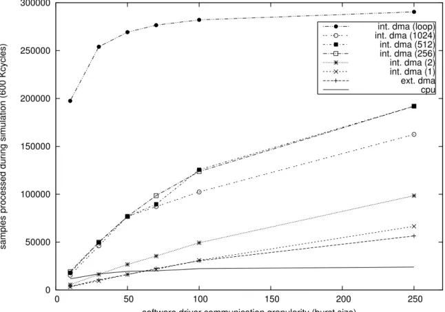
For thecpudriven platform the cache size has a strong effect on performance. For instance, in Fig. 7, we have shown the influence of cache line size on the frequency at which data could arrive to theip. The use of cache line of 16 bus word increases the throughput and the effect of a cache miss can be clearly visualised. With cache line reduced to one bus word, the data arrive regularly but slower. On the other hand it can be shown that cache size does not influence performances on this application as cache are direct-mapped. The behavior shown in Fig. 7 clearly indicate that efficient handling of burst mode through a dmamodule is a crucial issue to obtain an efficient use of the hardware accelerator. However, as it can be seen in table 1, performance for thedma engine are counterbalanced by the interrupt acknowledge mechanism that reduces the gain obtained with burst communications for small burst sizes. This tradeoff quickly turns in favour of thedmaplatform for burst sizes larger than 70 bus words on our architecture. As soon as the burst sizes counterbalance the interrupt latency thedmaplatform is more efficient thancpu driven I/O as it can be seen on figure Fig. 8 (ext. dma).
Using an externaldmamodule allows more efficient burst communications over the interconnect but still requires 4 transfers for each samples. The third architecture uses an internal dmathat has been implemented directly in the interface. This dma engine allows the interface to directly access the memory to fetch its input samples and to write the results back to the memory in only 2 accesses to the interconnect, reducing the number of data transfers by a factor 2 compared to the externaldmaplatform. Hardware accelerator throughput is not changed by using an internaldma for small burst sizes as the main bottleneck is still the transfer ofdmaconfigurations and interrupt handling. Hardware throughput for internaldmais shown on figure Fig. 8 (int. dma(1)).
The next architecture modification we have made is to use a scatter/gather enableddmaengine that can store several successive transfer configurations. This list reduces the number of interrupt that are generated by the dma. For instance, a list size of nconfigurations allows to reduce by a
0 50000 100000 150000 200000 250000 300000 0 50 100 150 200 250
samples processed during simulation (600 Kcycles)
software driver communication granularity (burst size)
cpu ext. dma int. dma (1) int. dma (2) int. dma (256) int. dma (512) int. dma (1024)int. dma (loop)
Figure 8. Hardware accelerator throughput according to different burst length and
cpu
or
dma
communication mechanism
factornthe number of interrupt acknowledge handled by thecpu. Performance improvements can be seen on figure Fig. 8 for several list size varying between 1 and 1024 configurations (int. dma(1 -- 1024)). Even when using big list sizes, performances ares still not at the maximum throughput, thecpustill has to perform configuration transfers using the bus. The more configuration thedma can store, the more transfers have to be done between two successive run of the accelerator. These inactivity periods occurring between burst mode computation phases introduce some extra latency that freezes the hardware pipeline during reconfiguration and have to be taken into account for real-time processing that have strict timing or jitter constraints on the data streams. Furthermore, the performance improvement is limited by the configuration transfers and we can observe a maximum performance between 256 and 512 configuration list sizes followed by a performance decrease for bigger lists. This performance decrease comes from the latency introduced by long configurations that cannot be fully completed during the 600 000 cycles of the simulation.
The last architecture we simulated overcomes the configuration problem by storing and trans-ferring the completeconfiguration to the internal dmausing a compact representation. This con-figuration represents the phases and motifs discussed in section 3. The loop enable dmathat we use in the architecture can perform the complete processing transfer without requiring interrupt for configuration transfers. This communication mode is close to the maximum theoretical throughput even for small burst sizes and is thus limited only by the interconnect bandwidth and memory per-formances. Furthermore, this high throughput is obtained for small burst sizes and allows to keep latency and jitter to a minimum compared to similar performances obtained with other solutions using big configuration lists. The performance results of Fig.8 clearly demonstrates that the loop enabledmais mandatory to reach interesting performances with a data-flowips on a SoC.
5. Related work
Many recent works present SoC simulation environments [18, 4, 14]. These approaches do not have an Open Source policy as the one of SocLib, their main concern is the acceleration of the simulation at various level of precision: transaction level or cycle accurate level. These works do not propose generic interface mechanism for ips. Some attempt have been made to abstract communication behaviour at high level [6] or at low level [26, 25, 2], but none of these approaches use the assumption that theipare in the data-flow model hence they propose solutions which are not optimised for stream processing.
Many of the interesting results in this field are based on the work of the Ptolemy project [17] and especially the introduction of various computation models for data-flow ips: process network [16] orsdf[27, 15]. An interesting theory has been developed for multi-rateip-based systems [12], but the problem solved is the interconnection between several data-flow ipwhile we specifically target a single data-flowipcontrolled by a host. The work presented here has its roots in the research on themmalpha system [8, 9], a very similar problem was studied by Park and Diniz [19, 20] leading to the design of a generic interface that can be parameterised to connect to different data-flowip with some constraints on theips. This approach does not assume that communications are known statically and propose a run-time resolution to solve conflicting access to the bus.
Several high level design tools are now clearly identified either as research prototypes or industrial products [11, 5, 24, 13, 16, 3], each of these tools have implemented ad-hoc communication protocol between the generated data-flowipand the host. The Pico [24] tool and the Paro tool [3] have in house interface mechanisms with dedicated solution for the problem exposed here. We expect our model to be usable at least bymmalpha and Gaut [5].
6
Conclusion
In this paper we have delimited a class of architecture that is subject to high throughput require-ment and restricted enough to allow an interface mechanism which is generic and efficient. The notion of phase, motif and pattern can be defined for many data flowipand are particularly useful for high level design tools that can use them to generate hardware and software interfaces together with theip.
The cycle accurate simulation environment that we use is much more accurate than theoretical estimation of throughput because cache behaviour and interruption handling are very difficult to predict. We have highlighted an important issue: a very important improvement in the throughput between the memory and theipcan be obtained with a slightly optimised version of scatter-gather dmathat we calledloop-enable dma. We have shown that the hardware/software of the interface can be generated automatically together with theipand quasi-optimal communication throughput can be reached.
References
[1] VSI Alliance. Virtual component interface standard (OCB specification 2, version 1.0), 2000. [2] N. Banerjee, P. Vellanki, and K.S. Chatha. A power and performance model for
network-on-chip architectures. InDesign, Automation and Test in Europe Conference (DATE), Paris, France, March 2004.
[3] M. Bednara and J. Teich. Automatic synthesis of FPGA processor arrays from loop algorithms.
[4] M. Bolado, H. Posadas, J. Castillo1, P. Huerta1, P. S´anchez1, C. S´anchez, H. Fouren, and F. Blasco. Platform based on open-source cores for industrial applications. InDesign, Automa-tion and Test in Europe Conference (DATE), Paris, France, March 2004.
[5] E. Casseau, C. Jego, and E. Martin. Architectural synthesis of digital processing applica-tions dedicated to submicron technologies. InIEEE International Conference on Electronics, Circuits, and Systems (ICECS 01), pages 533–536, 2001.
[6] V. Chandras, A. Xu, H. Schmit, and L. Pileggi. An interconnect channel design methodology for high performance integrated circuits. InDesign, Automation and Test in Europe Conference (DATE), Paris, France, March 2004.
[7] Alain Darte, Steven Derrien, and Tanguy Risset. Hardware/software interface for multi-dimensional processor arrays. In IEEE International Conference on Application-specific Sys-tems, Architectures and Processors (ASAP). IEEE Computer Society Press, 2005.
[8] S. Derrien, A. C. Guillou, P. Quinton, T. Risset, and C. Wagner. Automatic synthesis of efficient interfaces for compiled regular architectures. In Internationnal Samos Workshop on Systems, Architectures, Modeling and Simulation (Samos), Samos, Grece, July 2002.
[9] S. Derrien and T. Risset. Interfacing compiled FPGA programs: the MMAlpha approach. In A. Arabnia, editor,PDPTA2000: Second International Workshop on Engineering of Reconfig-urable Hardware/Software Objects. CSREA Press, June 2000.
[10] A. Fraboulet, T. Risset, and Antoine Scherrer. Cycle accurate simulation model generation for SoC prototyping. Technical Report 2004-18, LIP, ENS-Lyon, May 2004.
[11] A.-C. Guillou, P. Quinton, T. Risset, C. Wagner, and D. Massicotte. High level design of digital filters in mobile communications. Technical Report 1405, Irisa, June 2001.
[12] J. Horstmannshoff, T. Grotker, and H. Meyr. Mapping multirate dataflow to complex RT level hardware models. InIEEE International Conference on Application-Specific Array Processors (ASAP), pages 283–293., 1997.
[13] B. Hounsell and R. Taylor. Co-processor synthesis a new methodology for embedded software acceleration. In Design, Automation and Test in Europe Conference and Exhibition (DATE Designers’ Forum), Paris, France, March 2004.
[14] H.A. Jang, M. Kang, M.J. Lee, K. Chae, K. Lee, and K. Shim. High-level system modeling and architecture exploration with systemc on a network SoC: S3C2510 case study. InDesign, Automation and Test in Europe Conference (DATE), Paris, France, March 2004.
[15] Hyunuk Jung, Kangnyoung Lee, and Soonhoi Ha. Efficient hardware controller synthesis for synchronous dataflow graph in system level design. In International Symposium on System Synthesis (ISSS), pages 79–84, 2000.
[16] B. Kienhuis, E. Rijpkema, and E.F. Deprettere. Compaan: Deriving process networks from matlab for embedded signal processing architectures. In8th International Workshop on Hard-ware/Software Codesign (CODES), 2000.
[17] E.A. Lee et al. Overview of the Ptolemy project. Technical Report UCB/ERL No. M99/37, University of California, Berkeley, july 1999.
[18] M. Loghiy, F. Angiolini, D. Bertozzi, L. Benini, and R. Zafalon. Analyzing on-chip commu-nication in a MPSoC environment. In Design, Automation and Test in Europe Conference (DATE), Paris, France, March 2004.
[19] Joonseok Park and Pedro C. Diniz. Synthesis of pipelined memory access controllers for streamed data applications on FPGA-based computing engines. InInternational Symposium on System Synthesis (ISSS), pages 221–226, 2001.
[20] Joonseok Park and Pedro C. Diniz. Synthesis and estimation of memory interfaces for FPGA-based reconfigurable computing engines. InInternational Symposium on FPGA Custom Com-puting Machines, 2003.
[21] D. Gracia P´erez, G. Mouchard, and O. Temam. A new optimized implementation of the systemC engine using acyclic scheduling. InDesign, Automation and Test in Europe Conference and Exhibition (DATE Designers’ Forum), Paris, France, March 2004.
[22] Fr´ederic P´etrot, Denis Hommais, and Alain Greiner. A simulation environment for core based embedded systems. InAnnual Simulation Symposium, pages 86–91, Atlanta, GA, U.S.A, April 1997.
[23] P. Quinton, S. V. Rajopadhye, and T. Risset. On manipulating Z-polyhedra using a canonical representation. Parallel Processing Letters, 7(2):181–194, June 1997.
[24] R. Schreiber et al. High-Level Synthesis of Non Programmable Hardware Accelerators. In
IEEE International Conference on Application-specific Systems, Architectures and Processors (ASAP), Boston, July 2000.
[25] C. Shin, Y. Kim, E. Chung, K. Choi J. Kong, and S. Eo. Fast exploration of parameterized bus architecture for communication-centric SoC design. In Design, Automation and Test in Europe Conference (DATE), Paris, France, March 2004.
[26] V. D. silva, S. Ramesh, and A. Sowmya. Synchronous protocol automata: A framework for modelling and verification of SoC communication architectures. In Design, Automation and Test in Europe Conference (DATE), Paris, France, March 2004.
[27] M.C. Williamson. Synthesis of parallel hardware implementations from synchronous dataflow graph specifications. PhD thesis, University of California, Berkeley, CA, 1998.