LogiCORE IP Block
Memory Generator
v7.3
Product Guide
SECTION I: SUMMARY
IP Facts
Chapter 1: Overview
Feature Summary. . . 7
Native Block Memory Generator Feature Summary . . . 9
AXI4 Interface Block Memory Generator Feature Summary . . . 12
Applications . . . 27
Licensing and Ordering Information . . . 27
Chapter 2: Product Specification
Performance. . . 29Resource Utilization. . . 29
Port Descriptions . . . 38
Chapter 3: Designing with the Core
General Design Guidelines . . . 46Clocking. . . 87
Resets . . . 87
SECTION II: VIVADO DESIGN SUITE
Chapter 4: Customizing and Generating the Core
GUI . . . 89Generating the AXI4 Interface Block Memory Generator Core . . . 100
Output Generation. . . 103
Chapter 5: Constraining the Core
Required Constraints . . . 107Clock Placement . . . 107
Banking . . . 108
Transceiver Placement . . . 108
I/O Standard and Placement. . . 108
Chapter 6: Detailed Example Design
Directory and File Contents. . . 109Example Design . . . 109
SECTION III: ISE DESIGN SUITE
Chapter 7: Customizing and Generating the Core
GUI . . . 111Parameter Values in the XCO File . . . 127
Output Generation. . . 129
Chapter 8: Constraining the Core
Required Constraints . . . 135Device, Package, and Speed Grade Selections. . . 135
Clock Frequencies . . . 135
Clock Management . . . 135
Clock Placement . . . 135
Banking . . . 135
Transceiver Placement . . . 136
I/O Standard and Placement. . . 136
Chapter 9: Detailed Example Design
Directory and File Contents. . . 137Example Design . . . 137
Demonstration Test Bench . . . 137
Implementation . . . 139
Simulation . . . 140
Messages and Warnings . . . 141
Appendix B: Migrating
Migration Overview . . . 144
Differences Between Cores . . . 145
Using the Migration Kit . . . 149
Migrating a Design Manually . . . 155
Appendix C: Debugging
Finding Help on Xilinx.com . . . 168Debug Tools . . . 169
Simulation Debug. . . 171
Hardware Debug . . . 171
Interface Debug . . . 172
Appendix D: Native Block Memory Generator Supplemental Information
Appendix E: Additional Resources
Xilinx Resources . . . 208References . . . 208
Technical Support . . . 208
Revision History . . . 209
SECTION I: SUMMARY
IP Facts
Overview
Product Specification
Designing with the Core
Introduction
The Xilinx LogiCORE ™ IP Block Memory Generator (BMG) core is an advanced memory constructor that generates area and
performance-optimized memories using embedded block RAM resources in Xilinx FPGAs. Users can quickly create optimized memories to leverage the performance and features of block RAMs in Xilinx FPGAs.
The BMG core supports both Native and AXI4 interfaces.
The Native interface BMG core configurations support the same standard BMG functions delivered by previous versions of the Block Memory Generator (up to and including version 4.3). Port interface names are identical.
The AXI4 interface configuration of the BMG core is derived from the Native interface BMG configuration and adds an industry-standard bus protocol interface to the core. Two AXI4 interface styles are available: AXI4 and AXI4-Lite.
Features
For details on the features of each interface, see
Feature Summary in Chapter 1.
LogiCORE IP Facts Table Core Specifics Supported
Device Family(1)
Zynq™-7000(2), Artix-7, Virtex®-7, Kintex®-7, Virtex-6, Virtex-5, Virtex-4, Spartan®-6, Spartan-3E/XA, Spartan-3/XA, Spartan-3A/3AN/3A DSP Supported
User Interfaces AXI4, AXI4-Lite
Resources See Table 2-2.
Provided with Core
Design Files Vivado: Structural NetlistISE: NGC Netlist Example
Design VHDL
Test Bench VHDL
Constraints
File Vivado: XDCISE: UCF
Simulation
Model Verilog and VHDL Behavioral(3) and Structural Supported
S/W Driver N/A
Tested Design Flows(4)
Design Entry Vivado™ Design Suite v2012.4(5) ISE™ Design Suite v14.4 Simulation Cadence Incisive Enterprise Simulator Mentor Graphics ModelSim Xilinx ISim
Synthesis Vivado Synthesis
XST Support
Provided by Xilinx @ www.xilinx.com/support
Notes:
1. For a complete listing of supported devices, see the release notes for this core.
2. Supported in ISE Design Suite implementations only. 3. Behavioral models do not precisely model collision behavior.
See Simulation Models, page 9 for details.
4. For the supported versions of the tools, see the Xilinx Design Tools: Release Notes Guide.
Overview
The Block Memory Generator core uses embedded Block Memory primitives in Xilinx FPGAs to extend the functionality and capability of a single primitive to memories of arbitrary widths and depths. Sophisticated algorithms within the Block Memory Generator core produce optimized solutions to provide convenient access to memories for a wide range of configurations.
The Block Memory Generator has two fully independent ports that access a shared memory space. Both A and B ports have a Write and a Read interface. In Zynq-7000, 7 series, Virtex-6, Virtex-5 and Virtex-4 FPGA architectures, each of the four interfaces can be uniquely configured with a different data width. When not using all four interfaces, the user can select a simplified memory configuration (for example, a Single-Port Memory or Simple Dual-Port Memory) to reduce FPGA resource utilization.
The Block Memory Generator is not completely backward-compatible with the discontinued legacy Single-Port Block Memory and Dual-Port Block Memory cores; for information about
the differences, see Appendix B, Migrating.
Feature Summary
Features Common to the Native Interface and AXI4 BMG Cores
• Optimized algorithms for minimum block RAM resource utilization or low power utilization
• Configurable memory initialization
• Individual Write enable per byte in Zynq ™-7000, Kintex ™-7, Virtex ®-7, Virtex-6, Virtex-5, Virtex-4, Spartan ®-6, and Spartan-3A/XA DSP with or without parity • Optimized VHDL and Verilog behavioral models for fast simulation times; structural
simulation models for precise simulation of memory behaviors
• Selectable operating mode per port: WRITE_FIRST, READ_FIRST, or NO_CHANGE • Smaller fixed primitive configurations are now possible in Spartan-6 devices with the
introduction of the new Spartan-6 device 9K primitives
• VHDL example design and demonstration test bench demonstrating the IP core design flow, including how to instantiate and simulate it
Native Block Memory Generator Specific Features
• Generates Single-port RAM, Simple Dual-port RAM, True Dual-port RAM, Single-port ROM, and Dual-port ROM
• Supports data widths from 1 to 4608 bits and memory depths from 2 to 9M words (limited only by memory resources on selected part)
• Configurable port aspect ratios for dual-port configurations and Read-to-Write aspect ratios in Virtex-6, Virtex-5, and Virtex-4 FPGAs
• Supports the built-in Hamming Error Correction Capability (ECC) available in
Zynq-7000, 7 series, Virtex-6 and Virtex-5 devices for data widths greater than 64 bits. Error injection pins in Zynq-7000, 7 series, and Virtex-6 allow insertion of single and double-bit errors
• Supports soft Hamming Error Correction (Soft ECC) in Zynq-7000, 7 series, Virtex-6, and Spartan-6 devices for data widths less than 64 bits.
• Option to pipeline DOUT bus for improved performance in specific configurations • Choice of reset priority for output registers between priority of SR (Set Reset) or CE
(Clock Enable) in Zynq-7000, 7 series, Virtex-6, and Spartan-6 families • Asynchronous reset in Spartan-6 devices
• Performance up to 450 MHz
AXI4 Interface Block Memory Generator Specific Features
• Supports AXI4 and AXI4-Lite interface protocols • AXI4 compliant Memory and Peripheral Slave types • Independent Read and Write Channels
• Zero delay datapath
• Supports registered outputs for handshake signals • INCR burst sizes up to 256 data transfers
• WRAP bursts of 2, 4, 8, and 16 data beats • AXI narrow and unaligned burst transfers • Simple Dual-port RAM primitive configurations • Performance up to 300 MHz
• Symmetric aspect ratios • Asynchronous active low reset
Simulation Models
The Block Memory Generator core provides two types of functional simulation models: • Behavioral Simulation Models (VHDL and Verilog)
• Structural/UniSim based Simulation Models (VHDL and Verilog)
The behavioral simulation models provide a simplified model of the core while the
structural simulation models (UniSim) are an accurate modeling of the internal structure of the core. The behavioral simulation models are written purely in RTL and simulate faster than the structural simulation models and are ideal for functional debugging. Moreover, the memory is modeled in a two-dimensional array, making it easier to probe contents of the memory.
The structural simulation model uses primitive instantiations to model the behavior of the core more precisely. Use the structural simulation model to accurately model memory collision behavior and 'x' output generation. Note that simulation time is longer and debugging may be more difficult. The Simulation Files options in the CORE Generator
Project Options determine the type of functional simulation models generated. Table 1-1
defines the differences between the two functional simulation models.
Native Block Memory Generator Feature
Summary
Supported Devices
Table 1-2 shows the families and sub-families supported by the Block Memory Generator.
Table 1-1: Differences between Simulation Models
Behavioral Models Structural Models (Unisim) When core output is undefined Never generates ‘X’ Generates ‘X’ to match core Out-of-range address access Optionally flags a warning message Generates ‘X’
Collision behavior Does not generate ‘X’ on output, and flags a warning message Generates ‘X’ to match core Byte-Write collision behavior Flags all byte-Write collisions Does not flag collisions if byte-writes do not overlap
Memory Types
The Block Memory Generator core uses embedded block RAM to generate five types of memories:
• Single-port RAM • Simple Dual-port RAM • True Dual-port RAM • Single-port ROM • Dual-port ROM
For dual-port memories, each port operates independently. Operating mode, clock
frequency, optional output registers, and optional pins are selectable per port. For Simple
Dual-port RAM, the operating modes are not selectable. SeeCollision Behavior, page 59 for
additional information.
Selectable Memory Algorithm
The core configures block RAM primitives and connects them together using one of the following algorithms:
• Minimum Area Algorithm: The memory is generated using the minimum number of block RAM primitives. Both data and parity bits are utilized.
Table 1-2: Supported FPGA Families and Sub-Families
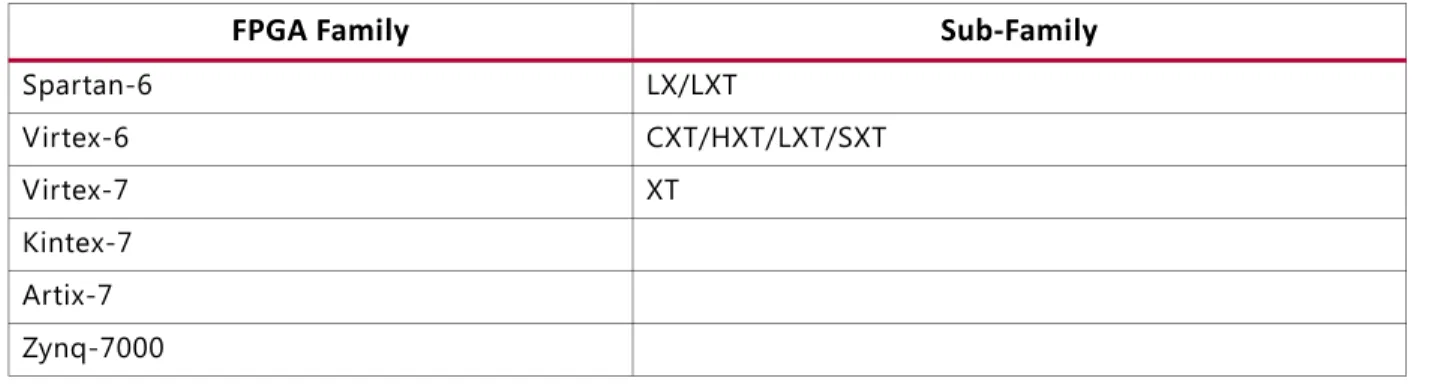
FPGA Family Sub-Family
Spartan-3 Spartan-3E Spartan-3A Spartan-3AN Spartan-3A DSP Spartan-6 LX/LXT Virtex-4 LX/FX/SX Virtex-5 LXT/FXT/SXT/TXT Virtex-6 CXT/HXT/LXT/SXT Virtex-7 XT Kintex-7 Artix ™-7 Zynq-7000
• Low Power Algorithm: The memory is generated such that the minimum number of block RAM primitives are enabled during a Read or Write operation.
• Fixed Primitive Algorithm: The memory is generated using only one type of block RAM primitive. For a complete list of primitives available for each device family, see the data sheet for that family.
Configurable Width and Depth
The Block Memory Generator can generate memory structures from 1 to 4096 bits wide, and at least two locations deep. The maximum depth of the memory is limited only by the number of block RAM primitives in the target device.
Selectable Operating Mode per Port
The Block Memory Generator supports the following block RAM primitive operating modes: WRITE FIRST, READ FIRST, and NO CHANGE. Each port may be assigned its own operating mode.
Selectable Port Aspect Ratios
The core supports the same port aspect ratios as the block RAM primitives:
• In all supported device families, the A port width may differ from the B port width by a factor of 1, 2, 4, 8, 16, or 32.
• In Zynq-7000, 7 series, Virtex-6, Virtex-5 and Virtex-4 FPGA-based memories, the Read width may differ from the Write width by a factor of 1, 2, 4, 8, 16, or 32 for each port.
The maximum ratio between any two of the data widths (DINA, DOUTA, DINB, and
DOUTB) is 32:1.
Optional Byte-Write Enable
In Zynq-7000, 7 series, Virtex-6, Virtex-5, Virtex-4, Spartan-6, and Spartan-3A/3A DSP FPGA-based memories, the Block Memory Generator core provides byte-Write support for memory widths which are multiples of eight (no parity) or nine bits (with parity).
Optional Output Registers
The Block Memory Generator provides two optional stages of output registering to increase memory performance. The output registers can be chosen for port A and port B separately. The core supports the Zynq-7000, 7 series, Virtex-6, Virtex-5, Virtex-4, Spartan-6, and Spartan-3A DSP embedded block RAM registers as well as registers implemented in the
FPGA fabric. See Output Register Configurations, page 187 for more information about
Optional Pipeline Stages
The core provides optional pipeline stages within the MUX, available only when the registers at the output of the memory core are enabled and only for specific configurations. For the available configurations, the number of pipeline stages can be 1, 2, or 3. For
detailed information, see Optional Pipeline Stages, page 64.
Optional Enable Pin
The core provides optional port enable pins (ENA and ENB) to control the operation of the
memory. When deasserted, no Read, Write, or reset operations are performed on the respective port. If the enable pins are not used, it is assumed that the port is always enabled.
Optional Set/Reset Pin
The core provides optional set/reset pins (RSTA and RSTB) for each port that initialize the
Read output to a programmable value.
Memory Initialization
The memory contents can be optionally initialized using a memory coefficient (COE) file or
by using the default data option. A COE file can define the initial contents of each individual
memory location, while the default data option defines the initial content of all locations.
Hamming Error Correction Capability
Simple Dual-port RAM memories support the built-in FPGA Hamming Error Correction Capability (ECC) available in the Zynq-7000, 7 series, Virtex-6 and Virtex-5 FPGA block RAM primitives for data widths greater than 64 bits. The BuiltIn_ECC (ECC) memory automatically detects single- and double-bit errors, and is able to auto-correct the single-bit errors. For data widths of 64 bits or less, a soft Hamming Error Correction implementation is available for Zynq-7000, 7 series, Virtex-6, and Spartan-6 designs.
AXI4 Interface Block Memory Generator Feature
Summary
Overview
AXI4 Interface Block Memories are built on the Native Interface Block Memories (see
supported by the Native Interface Block Memories, AXI4 Block Memories can also be used in AXI4 System Bus applications and Point-to-Point applications.
All communication in the AXI protocol is performed using five independent channels. Each of the five independent channels consists of a set of information signals and uses a two-way
VALID and READY handshake mechanism. The information source uses the VALID signal to
show when valid data or control information is available on the channel. The information
destination uses the READY signal to show when it can accept the data.
In Figure 1-2, the information source generates the VALID signal to indicate when data is
available.
The destination generates the READY signal to indicate that it can accept the data, and
transfer occurs only when both the VALID and READY signals are high.
The AXI4 Block Memory Generator is an AXI4 endpoint Slave IP and can communicate with multiple AXI4 Masters in an AXI4 System or with Standalone AXI4 Masters in point to point applications. The core supports Simple Dual Port RAM configurations. Because AXI4 Block Memories are built using Native interface Block Memories, they share many common features.
X-Ref Target - Figure 1-1
Figure 1-1: AXI4 Interface BMG Block Diagram
X-Ref Target - Figure 1-2
Figure 1-2: AXI4 Interface Handshake Timing Diagram 1$7,9( %0* &25( $;, ,17(5)$&( :5,7()60 $;, ,17(5)$&( 5($')60 $:9$/,' $:5($'< &+$11(/,1)2 :9$/,' :5($'< &+$11(/,1)2 %9$/,' %5($'< &+$11(/,1)2 :5,7($''5(66 &+$11(/ :5,7('$7$ &+$11(/ :5,7(5(63 &+$11(/ $;,0$67(5 :5,7(&+$11(/6 5($'$''5(66 &+$11(/ 5($''$7$ &+$11(/ $;,0$67(5 5($'&+$11(/6 $59$/,' $55($'< &+$11(/,1)2 59$/,' 55($'< &+$11(/,1)2 5($'< ,1)250$7,21 ;;; ,1)2 ;;; ,1)2 9$/,' $&/. ,1)2 ;;; ;
All Write operations are initiated on the Write Address Channel (AW) of the AXI bus. The AW channel specifies the type of Write transaction and the corresponding address information. The Write Data Channel (W) communicates all Write data for single or burst Write
operations. The Write Response Channel (B) is used as the handshaking or response to the Write operation.
On Read operations, the Read Address Channel (AR) communicates all address and control information when the AXI master requests a Read transfer. When the Read data is available to send back to the AXI master, the Read Data Channel (R) transfers the data and status of the Read operation
Applications
AXI4 Block Memories - Memory Slave Mode
AXI4 Block Memories in Memory Slave mode are optimized for Memory Mapped System Bus implementations. The AXI4 Memory Slave Interface Type supports aligned, unaligned or narrow transfers for incremental or wrap bursts.
Figure 1-3 shows an example application for the AXI4 Memory Slave Interface Type with an AXI4 Interconnect for Multi Master AXI4 applications. Minimum memory requirement for this configuration is set to 4K bytes. Data widths supported by this configuration include 32, 64, 128 or 256 bits
AXI4-Lite Block Memories - Memory Slave Mode
AXI4-Lite Block Memories in Memory Slave mode are optimized for the AXI4-Lite interface. They can be used in implementations requiring simple Control/Status Accesses. AXI4-Lite Memory Slave Interface Type supports only single burst transactions.
X-Ref Target - Figure 1-3
Figure 1-3: AXI4 Memory Slave Application Diagram
$;,0DVWHU $;,0DVWHU
$;,,QWHUFRQQHFW
$;,0DVWHU
$;,%0*
Figure 1-4 shows an example application for AXI4-Lite Memory Slave Interface Type with an AXI4-Lite Interconnect to manage Control/Status Accesses. The minimum memory
requirement for this configuration is set to 4K bytes. Data widths of 32 and 64 bits are supported by this configuration.
AXI4 Block Memories - Peripheral Slave Mode
AXI4 Block Memories in Peripheral Slave mode are optimized for a system or applications requiring data transfers that are grouped together in packets. The AXI4 Peripheral Slave supports aligned /unaligned addressing for incremental bursts.
Figure 1-5 shows an example application for the AXI4 Peripheral Slave Interface Type in a Point-to-point buffered link list application. There is no minimum memory requirement set for this configuration. Data widths supported by this configuration include 8, 16, 32, 64, 128 and 256 bits.
X-Ref Target - Figure 1-4
Figure 1-4: AXI4-Lite Memory Slave Application Diagram
X-Ref Target - Figure 1-5
Figure 1-5: AXI4 Peripheral Slave Application Diagram
3URFHVVRU3HULSKHUDO ,QWHUIDFH $;,/LWH,QWHUFRQQHFW $;,/,7(%0* 0(025<6/$9(02'( $;,/,7(6/$9( $;,/,7(6/$9( $;,0DVWHU :ULWH&KDQQHOV $;,0DVWHU 5HDG&KDQQHOV $;,%0* 3(5,3+(5$/6/$9( 02'( %XIIHU$GGU&RQWURO1H[W3WU %XIIHU %XIIHU %XIIHU$GGU&RQWURO1H[W3WU
AXI4-Lite Block Memories - Peripheral Slave Mode
AXI4-Lite Block Memories in Peripheral Slave mode are optimized for the AXI4-Lite interface. They can be used in implementations requiring single burst transactions.
Figure 1-8 shows an example application for the AXI4-Lite Memory Slave Interface Type in a Point-to-point application. There is no minimum memory requirement set for this
configuration. Data widths supported by this configuration include 8, 16, 32 and 64 bits.
Supported Devices
AXI4 BMG Core Channel Handshake Sequence
Figure 1-9 and Figure 1-10 illustrates an example handshake sequence for AXI4 BMG core.
Figure 1-9 illustrates single burst Write operations to block RAM. By default the AWREADY
signal is asserted on the bus so that the address can be captured immediately during the
clock cycle when both AWVALID and AWREADY are asserted. (With the default set in this
manner, there is no need to wait an extra clock cycle AWREADY to be asserted first.) By
default, the WREADY signal will be de-asserted. Upon detecting AWVALID being asserted,
the WREADY signal will be asserted (AXI4 BMG core has registered an AXI Address and is
ready to accept Data), and when WVALID is also asserted, writes will be performed to the
block RAM. If the write data channel (WVALID) is presented prior to the write address
X-Ref Target - Figure 1-6
X-Ref Target - Figure 1-74.2.4AXI4-Lite Block Memories - Peripheral Slave Mode X-Ref Target - Figure 1-8
Figure 1-8: AXI4-Lite Peripheral Slave Application Diagram
Table 1-3: AXI4 BMG Supported FPGA Families and Sub-Families
FPGA Family Sub-Family
Spartan-6 LX/LXT Virtex-6 CXT/HXT/LXT/SXT Virtex-7 XT Kintex-7 Artix-7 Zynq-7000 $;,/LWH0DVWHU :ULWH&KDQQHOV 5HDG&KDQQHOV $;,/,7( %0* 3(5,3+(5$/6/$9( 02'( 'DWD&RQWURO $;,/LWH0DVWHU
channel valid (AWVALID) assertion, the write transactions will not be initiated until the write
address channel has valid information.
The AXI4 Block Memory core will assert BVALID for each transaction only after the last data
transfer is accepted. The core also will not wait for the master to assert BREADY before
asserting BVALID.
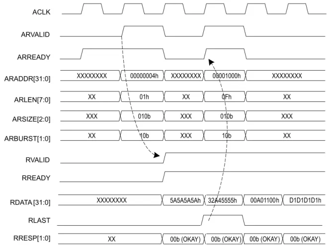
Figure 1-9 illustrates single burst Read operations to block RAM. The registered ARREADY
signal output on the AXI Read Address Channel interface defaults to a high assertion. The
AXI Read FSM can accept the read address in the clock cycle where the ARVALID signal is
first valid.
The AXI Read FSM can accept a same clock cycle assertion of the RREADY by the master if
the master can accept data immediately. When the RREADY signal is asserted on the AXI
bus by the master, the Read FSM will either negate the RVALID signal or will place next valid
data on the AXI Bus.
X-Ref Target - Figure 1-9
Figure 1-9: AXI4-Lite Single Burst Write Transactions :5($'< $:5($'< $:$''5>@ ;;;;;;;; K K ;;;;;;;; $:9$/,' $&/. :9$/,' :'$7$ >@ ;;;;;;;; )$$$K ;;%$$K ;;;;;;;; :675%>@ %5($'< %5(63>@ ;; %9$/,' ;;;; E E ;;;; ;; E2.$< E2.$<
For more details on AXI4 Channel handshake sequences refer to the “Channel Handshake”
section of the AXI protocol specification[Ref 1].
AXI4 Lite Single Burst Transactions
For AXI4 Lite interfaces, all transactions are burst length of one and all data accesses are the
same size as the width of the data bus. Figure 1-9 and Figure 1-10 illustrates timing of AXI
32-bit write operations to the 32-bit wide BRAM. Figure 1-9 example illustrates single burst
Write operations to block RAM addresses 0x1000h and 0x1004h. Figure 1-10 illustrates
single burst Read operations to block RAM addresses 0x1000h and 0x1004h.
AXI4 Incremental Burst Support
Figure 1-11 illustrates an example of the timing for an AXI Write burst of four words to a 32-bit block RAM. The address Write channel handshaking stage communicates the burst
type as INCR, the burst length of two data transfers (AWLEN = 01h). The Write burst utilizes
all byte lanes of the AXI data bus going to the block RAM (AWSIZE = 010b).
In compliance with AXI Protocol, the burst termination boundary for a transaction is
determined by the length specified in the AWLEN signal. The allowable burst sizes for INCR
bursts are from 1 (00h) to 256 (FFh) data transfers.
X-Ref Target - Figure 1-10
Figure 1-10: AXI4 Lite Single Burst Read Transactions
55($'< $55($'< $5$''5>@ ;;;;;;;; K ;;;;;;;; K ;;;;;;;; $59$/,' $&/. 59$/,' 5'$7$ >@ ;;;;;;;; )$$$K $$K ;;;;;;;; 55(63>@ ;;;;;;;; ;; E2.$< ;; E2.$< ;;
Figure 1-12 illustrates the example timing for an AXI Read burst with block RAM managed by the Read FSM. The memory Read burst starts at address 0x1000h of the block RAM. On the AXI Read Data Channel, the Read FSM enables the AXI master/Interconnect to respond
to the RVALID assertion when RREADY is asserted in the same clock cycle. If the requesting
AXI master/Interconnect throttles on accepting the Read burst data (by negating RREADY),
the Read FSM handles this by holding the data pipeline until RREADY is asserted.
X-Ref Target - Figure 1-11
Figure 1-11: AXI4 Incremental Write Burst Transactions
:5($'< $:5($'< $:$''5>@ ;;;;;;;; K ;;;;;;;; K ;;;;;;;; $:9$/,' $&/. $:/(1>@ ;; K ;;;;;;;; ))K ;; $:6,=(>@ ;;; E ;;;;;;;; E ;;; $:%8567>@ ;; E ;;;;;;;; E ;; :9$/,' :'$7$ >@ ;;;;;;;; ))))K $K $$$$K :/$67 :675%>@ %5($'< %5(63>@ ;; E2.$< ;; %9$/,' ;;$$$K ;;;; E E E E
AXI4 Wrap Burst Support
Cache line operations are implemented as WRAP burst types on AXI when presented to the
block RAM. The allowable burst sizes for WRAP bursts are 2, 4, 8, and 16. The AWBURST/
ARBURST must be set to “10” for the WRAP burst type.
WRAP bursts are handled by the address generator logic of the Write and Read FSM. The address seen by the block RAM must increment to the address space boundary, and then wrap back around to the beginning of the cache line address. For example, a processor issues a target word first cache line Read request to address 0x04h. On a 32-bit block RAM, the address space boundary is 0xFFh. So, the block RAM will see the following sequence of addresses for Read requests: 0x04h, 0x08h, 0x0Ch, 0x00h. Note the wrap of the cache line address from 0xCh back to 0x00h at the end.
X-Ref Target - Figure 1-12
Figure 1-12: AXI4 Incremental Read Burst Transactions
55($'< $55($'< $5$''5>@ ;;;;;;;; K K ;;;;;;;; $59$/,' $&/. $5/(1>@ ;; K ))K ;; $56,=(>@ ;;; E E ;;; $5%8567>@ ;; E E ;; 59$/,' 5'$7$ >@ 5/$67 55(63>@ ;;;;;;;; ))))K $$$K $K $$$$K
Figure 1-13 illustrates the timing for AXI Wrap or cache line burst transactions. The address generated and presented to the block RAM starts at the target word and wraps around once the address space boundary is reached.
Figure 1-14 illustrates the timing on AXI WRAP or cache line burst Read transactions.
X-Ref Target - Figure 1-13
Figure 1-13: AXI4 Wrap Write Burst Transactions :5($'< $:5($'< $:$''5>@ ;;;;;;;; K ;;;;;;;; $:9$/,' $&/. $:/(1>@ ;; K ;; $:6,=(>@ ;;; E ;;; $:%8567>@ ;; E ;; :9$/,' :'$7$ >@ ;;;;;;;; $$$$K $K :/$67 :675%>@ %5($'< %5(63>@ ;; %9$/,' $K ;;;; E E E E ''''K ;;; ;;;; E2.$<
Table 1-4 provides example address sequence to the block RAM for Wrap transactions.
For more details on AXI4 Wrap Burst Transactions and Wrap boundary calculations, refer to
the Burst Addressing section of the AXI protocol specification[Ref 1].
X-Ref Target - Figure 1-14
Figure 1-14: AXI4 Wrap Read Burst Transactions
Table 1-4: Example Address Sequence for AXI4 BMG Core Wrap Transactions Memory
Width Transfer Size
Start Address
Burst
Length AXI4 BMG Core Address Sequence 32-bits 32-bits 0x100Ch 2 0x100Ch(1), 0x1008h 32-bits 32-bits 0x1008h 4 0x1008h, 0x100Ch(1), 0x1000h, 0x1004h 64-bits 64-bits 0x1008h 8 0x1008h, 0x1010h, 0x1018h, 0x1020h, 0x1028h, 0x1030h, 0x1038h(1), 0x1000h 64-bits 16-bits 0x1008h 16 0x1008h, 0x100Ah, 0x100Ch, 0x100Eh, 0x1010, 0x1012, 0x1014, 0x1016h, 0x1018h, 0x101Ah, 0x101Ch, 0x101Eh(1), 0x1000h, 0x1002h, 0x1004h, 0x1006h
1. Calculated Wrap Boundary address. 55($'< $55($'< $5$''5>@ ;;;;;;;; K ;;;;;;;; K ;;;;;;;; $59$/,' $&/. $5/(1>@ ;; K ;; )K ;; $56,=(>@ ;;; E ;;; E ;;; $5%8567>@ ;; E ;;; E ;; 59$/,' 5'$7$ >@ 5/$67 55(63>@ ;;;;;;;; $$$$K $K $K ''''K
AXI4 Narrow Transactions
A narrow burst is defined as a master bursting a data size smaller than the block RAM data width. If the burst type (AWBURST) is set to INCR or WRAP, then the valid data on the block RAM interface to the AXI bus will rotate for each data beat. The Write and Read FSM handles each data beat on the AXI as a corresponding data beat to the block RAM, regardless of the smaller valid byte lanes. In this scenario, the AXI WSTRB is translated to the block RAM Write enable signals. The block RAM address only increments when the full address (data) width boundary is met with the narrow Write to block RAM.
Figure 1-15 illustrates an example of AXI narrow Write bursting with a 32-bit block RAM and the AXI master request is a half-word burst of four data beats. AWSIZE is set to 001b.
Figure 1-16 illustrates an example of AXI “narrow” Read bursting with a 32-bit block RAM and the AXI master request is a half-word burst of 4 data beats. ARSIZE is set to 001b.
X-Ref Target - Figure 1-15
Figure 1-15: AXI4 Narrow Write Burst Transactions
55($'< $55($'< $5$''5>@ ;;;;;;;; K ;;;;;;;; K ;;;;;;;; $59$/,' $&/. $5/(1>@ ;; K ;; K ;; $56,=(>@ ;;; E ;;; E ;;; $5%8567>@ ;; E ;; E ;; 59$/,' 5'$7$ >@ 5/$67 55(63>@ ;;;;;;;; '';;;;K ;;;;''K ;;;;;;K $;;;;;;K
For more details on AXI4 Narrow Transactions refer to the “Narrow transfers” section of the
AXI protocol specification[Ref 1].
AXI4 Unaligned Transactions
Unaligned burst transfers for example, occur when a 32-bit word burst size does not start on an address boundary that matches a word memory location. The starting memory address is permitted to be something other than 0x0h, 0x4h, 0x8h, etc. The example shown in Figure 1-17 illustrates an unaligned word burst transaction of 4 data beats, which starts at address offset, 0x1002h.
X-Ref Target - Figure 1-16
Figure 1-16: AXI4 Narrow Read Burst Transactions :5($'< $:5($'< $:$''5>@ ;;;;;;;; K ;;;;;;;; $:9$/,' $&/. $:/(1>@ ;; K ;; $:6,=(>@ ;;; E ;;; $:%8567>@ ;; E ;; :9$/,' :'$7$ >@ ;;;;;;;; '';;;;K '';;;;K :/$67 :675%>@ %5($'< %5(63>@ ;; %9$/,' ;;;;''K ;;;; E E E E ;;;;''K ;;;;;;;; ;;;; E2.$<
For more details on AXI4 Narrow Transactions refer to the “about unaligned transfers”
section of the AXI protocol specification[Ref 1].
Configurable Width and Depth
Table 1-5 provides supported Width and Depth for AXI4 Block Memory core.
For Peripheral Slave configurations, there is no minimum requirement for the number of address bits used by Block Memory core. For Memory Slave configuration, AXI4 Block Memory slave has at least sufficient address bits to fully decode a 4kB address range. For Peripheral Slave and AXI4 Lite Memory Slave configurations, AXI4 Block Memory core is not required to have low-order address bits to support decoding within the width of the system data bus and assumes that such low-order address bits have a default value of all zeros. For AXI4 Memory Slave configuration, AXI4 Block Memory core supports Narrow
Transactions and performs low-order address bits decoding. For more details, see AXI4
Interface Block Memory Addressing.
X-Ref Target - Figure 1-17
Figure 1-17: AXI4 Unaligned Transactions
Table 1-5: Supported Width and Depth Operating Mode Supported Memory Data Widths Supported Minimum Memory Depth
AXI4 Memory Slave 32,64,128, 256
Supports minimum 4kB address range: Data Width Minimum Depth 32 1024
64 512
128 256
256 128 AXI4 Lite Memory Slave 32,64
Supports minimum 4kB address range: Data Width Minimum Depth 32 1024 64 512
AXI4 Peripheral Slave 8, 16, 32,64,128, 256 2
AXI4 Lite Peripheral Slave 8, 16, 32,64, 2
' ' ' '
' ' ' '
' ' ' '
AXI4 Interface Block Memory Addressing
AXI4 Interface Block Memory cores support 32-bit byte addressing. There is no minimum requirement for the number of address bits supplied by a master. Typically a master is
expected to supply 32-bits of addressing. Table 1-6 illustrates some example settings to
create a specific size of block RAM in the system.
The Address Range of AXI Block Memory core must always start at zero. If the master has a different address bus width than that provided by the AXI4 Block Memory Core, follow these guidelines:
• If the Master address is wider than the configured Address Range for AXI Block
Memory core, the additional high-order address bits can be connected as is. AXI Block Memory core will ignore these bits.
• If the Master address is narrower than 32-bits, the high-order address bits of the AXI Block Memory core can be left unconnected.
For more details on AXI4 Addressing refer to the “Master Addresses” and “Slave Addresses”
section of the AXI protocol specification[Ref 1].
Throughput & Performance
To achieve 100 percent block RAM interface utilization of the Write port the following conditions must be satisfied.
• No single Write bursts.
• The AXI Master should not apply back pressure on the Write response channel
Table 1-6: AXI4 Interface Block Memory Generator Example Address Ranges Memory
Width x Depth MemorySize Address Range Required Base AddressExample Max AddressExample Block RAMAddress
8 x 4096 4K 0x0000_0000
to 0x0000_0FFF 0xA000 0000 0xA000 0FFF AXI_ADDR[11:0]
16 x 2048 4K 0x0000_0000
to 0x0000_0FFF 0xA000 0000 0xA000 0FFF AXI_ADDR[11:1]
32 x 1024 4K 0x0000_0000
to 0x0000_0FFF 0xA000 0000 0xA000 0FFF AXI_ADDR[11:2]
64 x 1024 8K 0x0000_0000 to 0x0000_1FFF 0x2400 0000 0x2400 1FFF AXI_ADDR[12:3] 128 x 1024 16K 0x0000_0000 to 0x0000_3FFF 0x1F00 0000 0x1F00 3FFF AXI_ADDR[13:4] 256 x 1024 32K 0x0000_0000 to 0x0000_7FFF 0x3000 0000 0x3000 7FFF AXI_ADDR[14:5]
To achieve 100 percent block RAM interface utilization of the Read port the following conditions must be satisfied.
• The AXI Master should not apply back pressure on the Read data channel
Selectable Port Aspect Ratios
The core currently supports only symmetric aspect ratios (that is, a 1:1 aspect ratio only).
Optional Output Register
The Output Register option is currently not supported.
Optional Pipeline Stages
Pipeline stages are currently not supported.
Memory Initialization Capability
The memory contents can be optionally initialized using a memory coefficient (COE) file or by specifying a default data value. A COE file can define the initial contents of each
individual memory location, while the default data value option defines the initial content for all locations.
Applications
The Block Memory Generator core is used to create customized memories to suit any application. Typical applications include:
• Single-port RAM: Processor scratch RAM, look-up tables • Simple Dual-port RAM: Content addressable memories, FIFOs • True Dual-port RAM: Multi-processor storage
• Single-port ROM: Program code storage, initialization ROM
• Dual-port ROM: Single ROM shared between two processors/systems
Licensing and Ordering Information
This Xilinx LogiCORE IP module is provided under the terms of the Xilinx Core License
Suite. For full access to all core functionalities in simulation and in hardware, you must
purchase a license for the core. Contact your local Xilinx sales representative for
information about pricing and availability.
For more information, visit the Block Memory Generator product page.
Information about other Xilinx LogiCORE IP modules is available at the Xilinx Intellectual
Property page. For information on pricing and availability of other Xilinx LogiCORE IP
Product Specification
This chapter includes details on performance and latency.
Performance
Performance and resource utilization for a BMG varies depending on the configuration and features selected during core customization.
See Resource Utilization for the performance and resource utilization numbers.
Latency
The latency of output signals of BMG varies for different configurations. See Optional
Output Registers, Optional Pipeline Stages, and Memory Output Flow Control in Chapter 3
for more details.
Resource Utilization
The following tables show resource utilization data and maximum performance values for a variety of sample BMG configurations.
Native Block Memory Generator Resource Utilization and
Performance Examples
Note: Benchmarking data for Virtex-7 and Kintex-7 devices will be available in future release.
The following tables provide examples of actual resource utilization and performance for Native Block Memory Generator implementations. Each section highlights the effects of a specific feature on resource utilization and performance. The actual results obtained will depend on core parameter selections, such as algorithm, optional output registers, and memory size, as well as surrounding logic and packing density.
Benchmarks were taken using a design targeting a Virtex-4 FPGA in the -10 speed grade (4VLX60-FF1148-10), Virtex-5 FPGA in the -1 speed grade (5VLX30-FF324-1), Virtex-6 FPGA
in the -1 speed grade (XC6VLX365T-FF1759-1) and a Spartan-6 FPGA in the -2 speed grade (XC6SLX150T-FGG484-2). All benchmarks were obtained using the ISE Design Suite. Better performance may be possible with higher speed grades.
In the benchmark designs described below, the core was encased in a wrapper with input and output registers to remove the effects of IO delays from the results; performance may vary depending on the user design. The minimum area algorithm was used unless otherwise noted. It is recommended that users register their inputs to the core for better performance. The following examples highlight the use of embedded registers in Virtex-4, Virtex-5, Virtex-6 and Spartan-6 devices, and the subsequent performance improvement that may result.
Single Primitive
The Block Memory Generator does not add additional logic if the memory can be
implemented in a single Block RAM primitive. Table 2-1 through Table 2-5 define
performance data for single-primitive memories.
Table 2-1: Single Primitive Examples - Virtex-7 FPGAs Memory
Type Options Width x Depth
Resource Utilization
Performance (MHz) Block RAMs Shift
Regs FFs LUTs 36K 18K True Dual-port RAM No Output Registers 36x512 1 0 0 0 0 414 9x2k 1 0 0 0 0 360 Embedded Output Registers 36x512 1 0 0 0 0 538 9x2k 1 0 0 0 0 454
Table 2-2: Single Primitive Examples - Virtex-6 FPGAs Memory Type Options Width x Depth Resource Utilization Performance (MHz) Block RAMs Shift
Regs FFs LUTsa
a. LUTs are reported as the number of 4-input LUTs, and do not reflect the number of LUTs used as a route-through. 36K 16K 8K True Dual-port RAM No Output Registers 36x512 1 0 0 0 0 0 325 9x2k 0 1 0 0 0 0 325 Embedded Output Registers 36x512 1 0 0 0 0 0 450 9x2k 0 1 0 0 0 0 450
Output Registers
The Block Memory Generator optional output registers increase the performance of memories by isolating the block RAM primitive clock-to-out delays and the data output multiplexer delays.
The output registers are only implemented for output ports. For this reason, when output registers are used, a Single-port RAM requires fewer resources than a True Dual-port RAM. Note that the effects of the core output registers are not fully illustrated due to the simple
Table 2-3: Single Primitive Examples - Virtex-5 FPGAs Memory Type Options Width x Depth Resource Utilization Performance (MHz) Block RAMs Shift
Regs FFs LUTsa
a. LUTs are reported as the number of 4-input LUTs, and do not reflect the number of LUTs used as a route-through. 36K 16K 8K True Dual-port RAM No Output Registers 36x512 1 0 0 0 0 0 300 9x2k 0 1 0 0 0 0 325 Embedded Output Registers 36x512 1 0 0 0 0 0 450 9x2k 0 1 0 0 0 0 450
Table 2-4: Single Primitive Examples - Virtex-4 FPGAs Memory
Type Options
Width x Depth
Resource Utilization Performance (MHz) Block
RAMs 16K
Shift
Regs FFs LUTsa
a. LUTs are reported as the number of 4-input LUTs, and do not reflect the number of LUTs used as a route-through. Virtex-4 True Dual-port RAM No Output Registers 36x512 1 0 0 0 300 9x2k 1 0 0 0 325 Embedded Output Registers 36x512 1 0 0 0 400 9x2k 1 0 0 0 400
Table 2-5: Single Primitive Examples - Spartan-6 FPGAs Memory Type Options Width x Depth Resource Utilization Performance (MHz) Block RAMs Shift
Regs FFs LUTsa
a. LUTs are reported as the number of 4-input LUTs, and do not reflect the number of LUTs used as a route-through. 36K 16K 8K True Dual-port RAM No Output Registers 36x512 0 1 0 0 0 0 200 9x2k 0 1 0 0 0 0 225 Embedded Output Registers 36x512 0 1 0 0 0 0 275 9x2k 0 1 0 0 0 0 300
register wrapper used. In a full-scale user design, core output registers may improve performance notably.
In Virtex-6, Virtex-5, Virtex-4, and Spartan-6 architectures, the embedded block RAM may be utilized, reducing the FPGA fabric resources required to create the registers.
Table 2-6: Virtex-6 Device Output Register Examples Memory Type Width x Depth Output Register Options
Block RAM Shift
Regs FFs LUTsa
a. LUTs are reported as the number of 4-input LUTs, and do not reflect the number of LUTs used as a route-through. Performance (MHz) 36K 16K 8K Single-por t RAM 17x5k 1 3 0 0 3 18 325 Primitive 1 3 0 3 3 18 450 Core 1 3 0 0 20 18 325 Primitive, Core 1 3 0 3 20 18 450 True Dual-port RAM 17x5k 1 3 0 0 6 36 300 Primitive 1 3 0 6 6 36 450 Core 1 3 0 0 40 36 300 Primitive, Core 1 3 0 6 40 36 450
Table 2-7: Virtex-5 Device Output Register Examples Memory Type Width x Depth Output Register Options
Block RAM Shift
Regs FFs LUTsa
a. LUTs are reported as the number of 4-input LUTs, and do not reflect the number of LUTs used as a route-through. Performance (MHz) 36K 16K 8K Single-por t RAM 17x5k 1 3 0 0 3 18 300 Primitive 1 3 0 3 3 18 450 Core 1 3 0 0 20 18 300 Primitive, Core 1 3 0 3 20 18 450 True Dual-port RAM 17x5k 1 3 0 0 6 36 300 Primitive 1 3 0 6 6 36 450 Core 1 3 0 0 40 36 300 Primitive, Core 1 3 0 6 40 36 450
Table 2-8: Virtex-4 Device Output Register Examples Memory
Type Width x Depth
Output Register Option Block RAMs 16K Shift
Regs FFs LUTsa Performance (MHz)
Single-por
t RAM 17x5k
- 5 0 3 30 275
Primitive 5 3 3 30 400
Aspect Ratios
The Block Memory Generator selectable port and data width aspect ratios may increase block RAM usage and affect performance, because aspect ratios limit the primitive types available to the algorithm, which can reduce packing efficiency. Large aspect ratios, such as 1:32, have a greater impact than small aspect ratios. Note that width and depth are reported with respect to the port A Write interface.
True Dual-port RAM 17x5k - 5 0 6 60 275 Primitive 5 6 6 148 375 Core 5 0 40 142 250 Primitive, Core 5 6 40 148 375
a. LUTs are reported as the number of 4-input LUTs, and do not reflect the number of LUTs used as a route-through. Table 2-9: Spartan-6 Device Output Register Examples
Memory
Type Width x Depth Output Register Options
Block RAM Shift
Regs FFs LUTsa
a. LUTs are reported as the number of 4-input LUTs, and do not reflect the number of LUTs used as a route-through. Performance (MHz) 36K 16K 8K Single-por t RAM 17x5k 0 5 0 0 3 19 175 Primitive 0 5 0 3 3 19 250 Core 0 5 0 0 20 19 175 Primitive, Core 0 5 0 3 20 19 225 True Dual-port RAM 17x5k 0 5 0 0 6 38 175 Primitive 0 5 0 4 6 38 250 Core 0 5 0 0 40 38 175 Primitive, Core 0 5 0 4 40 38 225
Table 2-10: Virtex-6 Device Aspect Ratio Memory Type Width x Depth Data Width Aspect Ratio Block RAMs
Shift Regs FFs LUTsa
a. LUTs are reported as the number of 4-input LUTs, and do not reflect the number of LUTs used as a route-through. Performance (MHz) 36K 16K 8K Single-por t RAM 17x5k 1:1 2 3 0 0 6 36 300 1:8b b. Read port is 136x640; Write port is 17x5k.
8 1 0 0 0 0 275
Table 2-8: Virtex-4 Device Output Register Examples Memory Type Width x Depth Output Register Option Block RAMs 16K Shift
Algorithm
The differences between the minimum area, low power and fixed primitive algorithms are
discussed in detail in Selectable Memory Algorithm, page 10. Table 2-13 shows examples of
the resource utilization and the performance difference between them for two selected configurations for Virtex-6 FPGA architectures.
Table 2-14 shows examples of the resource utilization and the performance difference between them for two selected configurations for Virtex-5 FPGA architecture.
Table 2-11: Virtex-5 Device Aspect Ratio Memory Type Width x Depth Data Width Aspect Ratio Block RAMs
Shift Regs FFs LUTsa
a. LUTs are reported as the number of 4-input LUTs, and do not reflect the number of LUTs used as a route-through. Performance (MHz) 36K 16K 8K Single-por t RAM 17x5k 1:1 2 3 0 0 6 36 300 1:8b b. Read port is 136x640; Write port is 17x5k.
8 1 0 0 0 0 275
Table 2-12: Virtex-4 Device Aspect Ratio Memory
Type Width x Depth
Data Width Aspect Ratio Block RAM 16K Shift Regs FFs LUTsa
a. LUTs are reported as the number of 4-input LUTs, and do not reflect the number of LUTs used as a route-through. Performance (MHz) Single
Port 17x5k
1:1 5 0 6 60 275
1:8b b. Read port is 136x640; Write port is 17x5k.
9 0 0 0 275
Table 2-13: Memory Algorithm Examples Virtex-6 Devices Memory Type Width x Depth Algorithm Type Block RAM
Shift Regs FFs LUTsa
a. LUTs are reported as the number of 4-input LUTs, and do not reflect the number of LUTs used as a route-through. Performance (MHz) 36K 16K 8K Single-po rt RAM 17x5k Minimum area 1 3 0 0 3 18 325 Fixed Primitive using 18x1k block RAM 2 1 0 0 3 19 300 Low power 0 5 0 0 3 37 275 36x4k Minimum area 4 0 0 0 0 0 325 Fixed Primitive using 36x512 block RAM 4 0 0 0 2 38 275 Low power 4 0 0 0 3 76 275
Table 2-15 shows examples of the resource utilization and the performance difference between them for two selected configurations for Virtex-4 FPGA architecture.
Table 2-16 shows examples of the resource utilization and the performance difference between them for two selected configurations for Spartan-6 FPGA architecture.
Table 2-14: Memory Algorithm Examples Virtex-5 Devices Memory Type Width x Depth Algorithm Type Block RAM
Shift Regs FFs LUTsa
a. LUTs are reported as the number of 4-input LUTs, and do not reflect the number of LUTs used as a route-through. Performance (MHz) 36K 16K 8K Single-po rt RAM 17x5k Minimum area 1 3 0 0 3 18 300 Fixed Primitive using 18x1k block RAM 2 1 0 0 3 20 300 Low power 0 5 0 0 3 39 275 36x4k Minimum area 4 0 0 0 0 0 300 Fixed Primitive using 36x512 block RAM 4 0 0 0 2 40 275 Low power 0 8 0 0 3 80 250
Table 2-15: Memory Algorithm Examples Virtex-4 Devices Memory
Type Width x Depth Algorithm Type
Resource Utilization
Performance (MHz) Block
RAM Shift Regs FFs LUTsa
a. LUTs are reported as the number of 4-input LUTs, and do not reflect the number of LUTs used as a route-through. Single-po rt RAM 17x5k Minimum area 5 0 3 30 275 Fixed Primitive using 18x1k block RAM 5 0 3 57 225 Low power 5 0 3 57 225 36x4k Minimum area 8 0 1 36 275 Fixed Primitive using 36x512 block RAM 8 0 3 152 225 Low power 8 0 3 152 225
AXI4 Block Memory Generator Resource Utilization and
Performance Examples
Note: Benchmarking data for Virtex-7 and Kintex-7 devices will be available in future release.
Table 2-17 through Table 2-20 show the resource utilization and performance data for a BMG core using the AXI4 interface. Benchmarks were taken using a design targeting a Virtex-6 FPGA in the -2 speed grade (XC6VCX75T-FF484-2) and a Spartan-6 FPGA in the -2 speed grade (XC6SLX150T-FGG484-2). All benchmarks were obtained using the ISE Design Suite. Better performance may be possible with higher speed grades.
In the benchmark designs, the core was encased in a wrapper with input and output registers to remove the effects of I/O delays from the results. Performance may vary depending on the design.
Table 2-16: Memory Algorithm Examples Spartan-6 Devices Memory Type Width x Depth Algorithm Type Block RAM
Shift Regs FFs LUTsa
a. LUTs are reported as the number of 4-input LUTs, and do not reflect the number of LUTs used as a route-through. Performance (MHz) 36K 16K 8K Single-po rt RAM 17x5k Minimum area 0 5 0 0 3 19 175 Fixed Primitive using 18x1k block RAM 0 5 0 0 3 37 175 Low power 0 0 10 0 4 57 150 36x4k Minimum area 0 8 0 0 1 18 175 Fixed Primitive using 36x512 block RAM 0 8 0 0 3 76 150 Low power 0 0 16 0 4 170 125
Table 2-17: AXI4 Block Memory Generator Virtex-6 FPGA Memory Type Options Width X Depth Resource Utilization Performance (MHz) Block RAMs
FFs LUTs OccupiedSlices 36K 16K 8K Simple Dual Port RAM Memory Slave 32x1024 1 0 0 92 207 74 306 64x512 1 0 0 95 225 81 282 Periphera l Slave 32x1024 1 0 0 52 151 53 320 64x512 1 0 0 50 145 46 299
Table 2-18: AXI4 Interface Block Memory Generator Spartan-6 FPGA Memory Type Options Width X Depth Resource Utilization Performance (MHz) Block RAMs
FFs LUTs OccupiedSlices
36K 16K 8K Simple Dual Port RAM Memory Slave 32x102 4 - 2 0 95 207 79 163 64x512 - 2 0 98 231 81 168 Periphera l Slave 32x102 4 - 2 0 56 159 57 175 64x512 - 2 0 54 149 51 165
Table 2-19: AXI4-Lite Block Memory Generator Virtex-6 FPGA Memory Type Options Width X Depth Resource Utilization Performance (MHz) Block RAMs
FFs LUTs OccupiedSlices
36K 16K 8K Simple Dual Port RAM Memory Slave 32x102 4 1 0 0 15 33 15 325 64x512 1 0 0 15 32 14 317 Periphera l Slave 32x102 4 1 0 0 15 33 15 335 64x512 1 0 0 15 32 14 317
Table 2-20: AXI4-Lite Interface Block Memory Generator Spartan-6 FPGA Memory Type Options Width X Depth Resource Utilization Performance (MHz) Block RAMs
FFs LUTs OccupiedSlices
36K 16K 8K Simple Dual Port RAM Memory Slave 32x102 4 - 2 0 25 45 18 219 64x512 - 2 0 24 43 20 217 Periphera l Slave 32x102 4 - 2 0 25 45 18 222 64x512 - 2 0 24 43 20 215
Port Descriptions
Native Block Memory Generator Signal List
Table 2-21 provides a description of the Block Memory Generator core signals. The widths
of the data ports (DINA, DOUTA, DINB, and DOUTB) are selected by the user in the CORE
Generator GUI. The address port (ADDRA and ADDRB) widths are determined by the memory
depth with respect to each port, as selected by the user in the GUI. The Write enable ports
(WEA and WEB) are busses of width 1 when byte-writes are disabled. When byte-writes are
enabled, WEA and WEB widths depend on the byte size and Write data widths selected in the
GUI.
Table 2-21: Core Signal Pinout
Name Direction Description
CLKA Input Port A Clocksynchronous operation, this must be driven by the same signal as : Port A operations are synchronous to this clock. For CLKB.
ADDRA Input Port A AddressWrite operations. Available in all configurations.: Addresses the memory space for port A Read and DINA Input Port A Data InputA. Available in all RAM configurations.: Data input to be written into the memory via port DOUTA Output Port A Data OutputAvailable in all configurations except Simple Dual-port RAM.: Data output from Read operations via port A. ENA Input Port A Clock Enableport A. Optional in all configurations.: Enables Read, Write, and reset operations via WEA Input Port A Write Enableall RAM configurations.: Enables Write operations via port A. Available in RSTA Input Port A Set/Resetregister. Optional in all configurations.: Resets the Port A memory output latch or output REGCEA Input Port A Register EnableOptional in all configurations with port A output registers.: Enables the last output register of port A.
CLKB Input Port B ClockAvailable in dual-port configurations. For synchronous operation, this : Port B operations are synchronous to this clock. must be driven by the same signal as CLKA.
ADDRB Input Port B addressWrite operations. Available in dual-port configurations.: Addresses the memory space for port B Read and DINB Input Port B Data InputB. Available in True Dual-port RAM configurations.: Data input to be written into the memory via port DOUTB Output Port B Data OutputAvailable in dual-port configurations.: Data output from Read operations via Port B. ENB Input Port B Clock EnablePort B. Optional in dual-port configurations.: Enables Read, Write, and reset operations via
AXI4 Interface Block Memory Generator Signal List
AXI4 Interface - Global Signals
AXI4-Interface Signals
WEB Input Port B Write EnableDual-port RAM configurations.: Enables Write operations via Port B. Available in RSTB Input Port B Set/Resetregister. Optional in all configurations.: Resets the Port B memory output latch or output REGCEB Input Port B Register EnableOptional in dual-port configurations with port B output registers.: Enables the last output register of port B. SBITERR Output Single-Bit Errorwhich has been auto-corrected on the output bus.: Flags the presence of a single-bit error in memory
DBITERR Output Double-Bit ErrorDouble-bit errors cannot be auto-corrected by the built-in ECC : Flags the presence of a double-bit error in memory. decode module.
INJECTSBITERR Input Inject Single-Bit Error: Available only for Zynq-7000, 7 series, and Virtex-6 ECC configurations.
INJECTDBITERR Input Inject Double-Bit Error: Available only for Zynq-7000, 7 series, and Virtex-6 ECC configurations.
RDADDRECC Output Read Address for ECC Error output: Available only for Zynq-7000, 7 series, and Virtex-6 ECC configurations.
Table 2-22: AXI4 or AXI4-Lite- Global Interface Signals
Name Direction Description
AXI4 or AXI4-Lite Global Interface Signals
S_ACLK Input Global Slave Interface Clockedge of this clock. : All signals are sampled on the rising S_ARESETN Input Global Reset: This signal is active low.
Table 2-23: AXI4 Write Channel Interface Signals
Name Direction Description
AXI4 Write Address Channel Interface Signals S_AXI_AWID[m:0] Input
Write Address ID: This signal is the identification tag for the Write address group of signals.
Write address ID is optional for Memory Slave configuration and is not supported for Peripheral Slave configuration.
Table 2-21: Core Signal Pinout (Cont’d)
S_AXI_AWADDR[31:0] Input
Write Address: The Write address bus gives the address of the first transfer in a Write burst transaction. The associated control signals are used to determine the addresses of the remaining transfers in the burst.
S_AXI_AWLEN[7:0] Input Burst Lengthin a burst. This information determines the number of data : The burst length gives the exact number of transfers transfers associated with the address.
S_AXI_AWSIZE[2:0] Input
Burst Size: This signal indicates the size of each transfer in the burst. Byte lane strobes indicate exactly which byte lanes to update. Burst size should always be less than or equal to the width of the Write Data.
Burst Size input is not supported for Peripheral Slave configuration.
S_AXI_AWBURST[1:0] Input
Burst Type: The burst type, coupled with the size information, details how the address for each transfer within the burst is calculated.
Burst type for Memory Slave configuration could be either incremental or wrap.
Burst type input is not supported for Peripheral Slave
configuration, Burst type for Peripheral Slave is always internally set to incremental.
S_AXI_AWVALID Input
Write Address Valid: This signal indicates that valid Write address and control information are available:
• 1 = address and control information available.
• 0 = address and control information not available. The address and control information remain stable until the address acknowledge signal, AWREADY, goes HIGH.
S_AXI_AWREADY Output
Write Address Ready: This signal indicates that the slave is ready to accept an address and associated control signals:
• 1 = Slave ready • 0 = Slave not ready
AXI4 Write Data Channel Interface Signals S_AXI_WDATA[m-1:0] Input
Write Data: For Memory Slave configurations, the Write data bus can be 32, 64, 128, or 256 bits wide. For Peripheral Slave
configurations, the Write data bus can be 8, 16, 32, 64, 128, or 256 bits wide.
S_AXI_WSTRB[m/8-1:0] Input
Write Strobes: This signal indicates which byte lanes to update in memory. There is one Write strobe for each eight bits of the Write data bus. Therefore, WSTRB[n] corresponds to WDATA[(8 × n) + 7:(8 × n)].
S_AXI_WLAST Input Write Last: This signal indicates the last transfer in a Write burst.
S_AXI_WVALID Input
Write Valid: This signal indicates that valid Write data and strobes are available:
• 1 = Write data and strobes available • 0 = Write data and strobes not available Table 2-23: AXI4 Write Channel Interface Signals (Cont’d)
S_AXI_WREADY Output
Write Ready: This signal indicates that the slave can accept the Write data:
• 1 = slave ready • 0 = slave not ready
AXI4 Write Response Channel Interface Signals
S_AXI_BID[m:0] Output
Response ID: The identification tag of the Write response. The BID value must match the AWID value of the Write transaction to which the slave is responding.
Response ID is optional for Memory Slave configuration and is not supported for Peripheral Slave configuration.
Response ID can be 1 to 16 bits wide.
S_AXI_BRESP[1:0] Output
Write Response: This signal indicates the status of the Write transaction. The allowable responses are OKAY, EXOKAY, SLVERR, and DECERR.
Write response is always set to OKAY.
Write response is generated only when AXI4 ID is enabled for Memory Slave. Write response is not supported for Peripheral Slave configuration.
S_AXI_BVALID Output
Write Response Valid: This signal indicates that a valid Write response is available:
• 1 = Write response available • 0 = Write response not available
S_AXI_BREADY Input
Response Ready: This signal indicates that the master can accept the response information.
• 1 = Master ready • 0 = Master not ready Table 2-24: AXI4 Read Channel Interface Signals
Name Direction Description
AXI4 Read Address Channel Interface Signals
S_AXI_ARID[m:0] Input
Read Address ID: This signal is the identification tag for the Read address group of signals.
Read address ID is optional for Memory Slave configuration and is not supported for Peripheral Slave configuration.
Read address ID can be 1 to 16 bits wide.
S_AXI_ARADDR[31:0] Input
Read Address: The Read address bus gives the initial address of a Read burst transaction.
Only the start address of the burst is provided and the control signals that are issued alongside the address detail how the address is calculated for the remaining transfers in the burst.
S_AXI_ARLEN[7:0] Input Burst Lengthin a burst. This information determines the number of data transfers : The burst length gives the exact number of transfers associated with the address.
Table 2-23: AXI4 Write Channel Interface Signals (Cont’d)
S_AXI_ARSIZE[2:0] Input
Burst Size: This signal indicates the size of each transfer in the burst.
Burst size should always be less than or equal to the width of the Read Data.
Burst Size input is not supported for Peripheral Slave configuration.
S_AXI_ARBURST[1:0] Input
Burst Type: The burst type, coupled with the size information, details how the address for each transfer within the burst is calculated.
Burst type for Memory Slave configuration could be either incremental or wrap.
Burst type input is not supported for Peripheral Slave configuration, Burst type for Peripheral Slave is always internally set to
incremental.
S_AXI_ARVALID Input
Read Address Valid: This signal indicates, when HIGH, that the Read address and control information is valid and will remain stable until the address acknowledge signal, ARREADY, is high.
• 1 = address and control information valid • 0 = address and control information not valid S_AXI_ARREADY Output
Read Address Ready: This signal indicates that the slave is ready to accept an address and associated control signals:
• 1 = slave ready • 0 = slave not ready
AXI4 Read Data Channel Interface Signals
S_AXI_RID[m:0] Output
Read ID Tag: This signal is the ID tag of the Read data group of signals. The RID value is generated by the slave and must match the ARID value of the Read transaction to which it is responding. Read ID tag is optional for Memory Slave configuration and is not supported for Peripheral Slave configuration.
Read ID can be 1 to 16 bits wide. S_AXI_RDATA[m-1:0] Output
Read Data: For Memory Slave configurations, the Read data bus can be 32, 64, 128, or 256 bits wide. For Peripheral Slave
configurations, the Read data bus can be 8, 16, 32, 64, 128, or 256 bits wide.
S_AXI_RRESP[1:0] Output
Read Response: This signal indicates the status of the Read transfer. The allowable responses are OKAY, EXOKAY, SLVERR, and DECERR. Read response is always set to OKAY.
Read response is generated only when AXI4 ID is enabled for Memory Slave. Read response is not supported for Peripheral Slave configuration.
S_AXI_RLAST Output Read Last: This signal indicates the last transfer in a Read burst. Table 2-24: AXI4 Read Channel Interface Signals (Cont’d)
AXI4-Lite Interface Signals
S_AXI_RVALID Output
Read Valid: This signal indicates that the required Read data is available and the Read transfer can complete:
• 1 = Read data available • 0 = Read data not available
S_AXI_RREADY Input
Read Ready: This signal indicates that the master can accept the Read data and response information:
• 1= Master ready • 0 = Master not ready
Table 2-25: AXI4-Lite Write Channel Interface Signals
Name Direction Description
AXI4-Lite Write Address Channel Interface Signals S_AXI_AWADDR[31:0] Input
Write Address: The Write address bus gives the address of the first transfer in a Write burst transaction. The associated control signals are used to determine the addresses of the remaining transfers in the burst.
S_AXI_AWVALID Input
Write Address Valid: This signal indicates that valid Write address and control information are available:
• 1 = address and control information available • 0 = address and control information not available. The address and control information remain stable until the address acknowledge signal, AWREADY, goes HIGH
S_AXI_AWREADY Output
Write Address Ready: This signal indicates that the slave is ready to accept an address and associated control signals:
• 1 = slave ready • 0 = slave not ready
S_AXI_AWID[m:0] Input
Write Address ID: This signal is the identification tag for the Write address group of signals
Write address ID is optional for Memory Slave configuration and is not supported for Peripheral Slave configuration.
Write address ID can be 1 to 16 bits wide. AXI4-Lite Write Data Channel Interface Signals
S_AXI_WDATA[m-1:0] Input Write Datacan be 32 or 64 bits wide. For Peripheral Slave configurations, the : For Memory Slave configurations, the Write data bus Write data bus can be 8, 16, 32 or 64 bits wide.
S_AXI_WSTRB[m/8-1:0] Input
Write Strobes: This signal indicates which byte lanes to update in memory. There is one Write strobe for each eight bits of the Write data bus. Therefore, WSTRB[n] corresponds to WDATA[(8 × n) + 7:(8 × n)].
Table 2-24: AXI4 Read Channel Interface Signals (Cont’d)
![Figure 3-17: Spartan-3 Block Memory: Register Port [A|B] Outputs of Memory Primitives and Memory Core Options Enabled](https://thumb-us.123doks.com/thumbv2/123dok_us/9690675.2457905/63.918.181.806.119.595/figure-spartan-memory-register-outputs-primitives-options-enabled.webp)
![Figure 3-18: Zynq-7000, 7 Series, Virtex-6, Virtex-5, and Virtex-4 Block Memory with Register Port [A|B] Output of Memory Primitives and Register Port [A|B] Output of](https://thumb-us.123doks.com/thumbv2/123dok_us/9690675.2457905/64.918.195.785.121.583/figure-series-virtex-virtex-virtex-register-primitives-register.webp)