INDO
INDO
–
–
GERMAN WINTER ACADEMY 2009
GERMAN WINTER ACADEMY 2009
Resistive Memory Devices
Harshit
Harshit
S.
S.
Vaishnav
Vaishnav
Outline
• Overview of Present Memory Technology - DRAM, SRAM, Flash Memory - Future Trends and Issues
• Resistive Memory Devices
- MRAM, PRAM, CBRAM, Organic Memory etc.
• Comparision
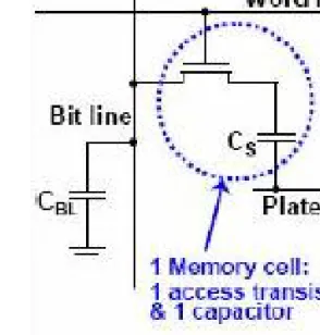
Dynamic RAM (DRAM
)
Principle: Data stored as presence/absence of charge on a capacitor
• Writing: Closing the switch (access transistor) and applying data (“1” or “0”) on the bit line
• Reading: Capacitor connected to bit line - Destructive readout due
to capacitive division
• Decrease of stored charge with time - Refreshing required
Fig 1: 1T-1C DRAM Cell
Advantages: Simplicity due to small cell size, high density, cheap
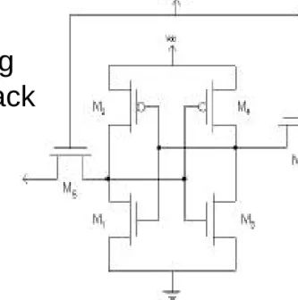
Static RAM (SRAM
)
Fig 2: 6T SRAM Cell
Principle: Data stored (actively held) using transistors in positive
feedback
• Most common : 6 transistors per cell
- 2 transistors used for reading and writing - Other 4 form inverters in positive feedback
and hold “1” or “0” till supply is present
• Writing: Activating bit line, feedback takes over
• Reading: Differential sense amplifier
Advantages: High speed, no refresh needed
Flash Memory
Principle: Data stored as presence or absence of charges inside gate
oxide of a MOS transistor causing the threshold voltage to be different
• A second gate electrode is used.
• Hot electron effect or “Fowler Nordheim tunelling” is used
Advantages: Non volatile, high retention, small cell size
Disadvantages: Low endurance, high writing time
Future Trends and Issues
• Limitations in each of today‘s memory technologies DRAM: Volatile, difficult integration
SRAM: Expensive, volatile, high power consumption Flash: Slow writing speed, insufficient writing cycles
• Limitations in charge-storage-based memories with further scaling of structural dimensions
• More complex fabrication because of constant down-scaling
• Need for a “Universal Memory” which has following characteristics:
- Non volatility with long retention time
- Low power consumption - High speed
- Compatibility with today’s Si technology
- High density and scalability - Low cost
Resistive Memory Devices
• Non volatile• Data written by changing some property of materials which changes the electrical resistance
• Reading by measuring resistance and comparing with reference
• Most promising candidates
- Magnetoresistive RAM (MRAM) - Phase Change RAM (PRAM) - Organic Memory
- Conductive Bridge RAM (CBRAM)
Magnetoresistive RAM (MRAM)
Principle: Storing information as direction of magnetization which
affects resistance offered to spin polarized current.
• Based on magnetic memory elements integrated with CMOS
• Uses a magnetic state for storage of data
- Each state offers different electrical resistance
• Reading by sensing the resistance without disturbing the state
• Two effects can be used for implementing an MRAM cell: - Giant Magnetoresistance (GMR)
• In layered magnetic structures, resistivity depends on relative alignment of
adjacent ferromagnetic layers
• Parallel magnetization: Low resistance
• Antiparallel magnetization: High resistance
• Explained by Motto’s two current model
- Two different channels for spin up and spin down electrons - Scattering process responsible for electrical resistance
• GMR < 40%
Giant Magnetoresistance (GMR)
• Two thin film ferromagnetic electrodes separated by barrier
• Small voltage: Quantum mechanical tunnel current - Overlap of wave functions
- Effect more prominent in thin films
• Tunneling resistance depends on relative magnetization on both sides of the barrier
• TMR % upto 50-60% have been shown for NiFe, NiFeCo,CoFe
• TMR has higher magnetoresistance % and hence is used to implement MRAM
• Magnetic Tunnel Junction (MTJ) MRAM cell
Tunnel Magnetoresistance (TMR)
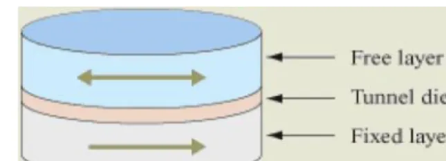
MRAM Cell
• MTJ consists of- Free layer : Magnetization changes with applied field
- Tunnel dielectric : Thin dielectric
- Fixed layer : Fixed magnetization
• When a bias is applied to MTJ, spin polarized electrons tunnel across the dielectric barrier.
- Resistance depends on stored data
• Hysteresis loop indicates memory - Magnetization in free layer is
retained after field is removed
Fig 6: MTJ
MRAM Cell – Reading and Writing
• For high density, MRAM cells are arranged ina 2D matrix
• Cells at crosspoints are selected using digit and bit lines
- Cells having only one line selected not written but “half-selected”
• Writing: Current pulses passed through bit line and digit line, writing the bit (changing magnetization of the free layer) at the cross point.
• Reading: Small sense current passed through the cell and compared with reference
Fig 8: Matrix of MRAM Cells
MRAM Cell - Switching
• Switching by Stoner-Wohlfrath reversal
• Points outside the astroid have only one stable state. They are “fully-selected”
• Points inside the astroid are “half- selected”
- Can get selected due to thermal noise or stray fields: errors
Hword Hbit “0” “1” Astroid : (Hword )2/3 + (H bit )2/3 = (H0 )2/3 (Ref: [5]) HS HS HS
• Drawback of Stoner – Wohlfrath MRAM is that margin between half-select and full-select is small
MRAM Characteristics
Advantages :
• Magnetic polarization doesn’t leak away with time
• No endurance limit
• High density and small access times
• Magnetic polarization switching doesn’t involve actual movement of electrons & so has no wear-out mechanism
Disadvantages:
• Integration of the magnetic stack is very critical due to exact thickness definition of insulating tunnel layer
• Induced field overlaps adjacent cells over a small area leading to false writes-half-select phenomenon
• Decrease in magnetic volume increases susceptibility to disturbs from thermal fluctuations or stray fields
Toggle-mode MRAM
• Free layer is replaced by Synthetic
Antiferromagnet (SAF), ferromagnetic sublayers of nearly same magnetic moment
- Net magnetic moment is very low and high magnetic volume is possible
• Write lines oriented 45° to easy axis
• Resistance determined by magnetization
direction of sense layer with respect to pinned layer
• Different response to magnetic fields than conventional free layer
Toggle-mode MRAM
• Two phase programming pulse sequence for 180° rotation, unipolar currents
• Toggling regardless of existing state
- Pre-read to determine if a write is required
• High bit-disturb margin, half write power
• Zero field orientation determined by intrinsic anisotropy • “Scissored” state between t1 and t4 . Net moment along applied field
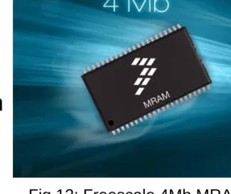
MRAM Current Status
• Commercially available: 4Mb chip @ 40MHz by EverSpin(Freescale), e2v
• 16Mb prototype presented by IBM and Infineon
• EverSpin (Freescale) intends to launch 16Mb chip soon
• Lot of research going on in academia and industry
• Leading companies are: Freescale, Intel, IBM, Toshiba, ST Microelectronics, Samsung
• Predicted by end of 2010: 64Mb and 128Mb chips
Fig 12: Freescale 4Mb MRAM Chip
Phase Change RAM (PRAM)
Principle: Storing information as phase of materials i.e either crystalline
or amorphous and reading by measuring the resistance.
• Uses phase change properties of chalcogenides (alloys of Group VI elements)
• At room temperature, chalcogenide alloys exist in two stable forms : crystalline and amorphous.
- Amorphous state has low free electron density and low electron mobility and hence has a high resistivity
- Crystalline state has high free electron density and high electron mobility and hence low resistance
• The state can be quickly and reversibly changed from one form to another
PRAM - Writing and Reading
• Basic material: Ge2 Sb2 Te5 (GST) alloy• Amorphization (Writing a “0”): The chalcogenide material is changed
into an amorphous state by first heating the material using joule heating above the melting point using a high current and then rapidly quenching it to prevent bonding.
• Crystallization (Writing a “1”): The material is crystallized by passing medium current for a longer time.
PRAM Contd …
• In the reset-set transition, a low current (~200uA) is passed for a long duration
• In the set-reset transition, a high current (~ 500uA) is passed for small duration
• Set-reset transition has to be fast enough to prevent recrystallization
• Reading is carried out by differentiating between high and low resistance states using a much lower current
PRAM Characteristics
Advantages
• Non volatile memory with retention period >10 years at 125oC
• Low voltage (<1.5V) operation and easily integrable with CMOS
• Large number of read-write cycles (>1013 )
• Large resistance drop, typically between 100 and 1000 - Larger swing for read circuitry
• Highly scalable, projected to be scalable beyond 22nm node
• Fast set and reset times
• Multiple bit storage is also possible, since resistance can be made to vary in reproducible steps
PRAM Characteristics
Disadvantages
• Large size, due to high current in set stage (~1mA) This is a big issue
• Ways of reducing writing current :
- Increasing resistance of GST module by nitrogen doping - Increasing heating efficiency
- Reducing heat dissipation
PRAM Current Status
• Numonyx to start volume production of 1Gbit PRAM chips by 2010 end
• Intel and Numonyx have already created a 64Mb chip
• Samsung produced 512Mb prototype which was 30 times faster than current Flash memory
• Leading companies are : Intel, Numonyx, Samsung, Toshiba, STMicroelectronics
Bistable Organic Memories
Principle: Utilizing conductance switching of organic complexes
• Reversible conductance switching is desirable because of relatively high resistance ratio between on and off states and non-destructive read
• No complicated stacks are involved
• Hybrid memory consists of conventional frontend-of- the-line
processing for CMOS circuit fabrication and memory layers added on the top
• Cross-point array cell array: two electrodes with memory element sandwiched between them
Bistable Organic Memories
• Organic resistive switch: two different resistance states: “0” and “1”
• Sandwich structure consisting of three layers between top and bottom metal electrodes
• Three layers are: organic semiconductor, metal and the organic semiconductor
Bistable Organic Memories
Advantages
• Simple integration, small size
• Properties of organic memory layers can be tailored by selective change of molecular structure
• Organic materials are suited for vacuum deposition and other processes, thereby reducing process complexity
• Good scalability, potential to be scalable to less than 20nm
Disadvantages
CBRAM
Principle: Utilizes the electrochemical formation and removal of metallic pathways in thin films of solid electrode to get low and high resistances
• Conducting path of metal atoms exists => Low R, otherwise high R.
Fig 18: Commonly used Programmable Metallization Cell (PMC) (Ref: [10])
• Anode is an oxidizable metal, solid electrolyte is Ag doped GexSe1-x and cathode is inert
• Redox reaction at anode : M = M+ + e
-CBRAM Working
• Positive voltage at the anode reduces the ions at the cathode to form metal atoms
• Positive ions are repelled from the anode into the solid
electrolyte.
• A conductive bridge of metal atoms is formed, which gives the low resistance ON state.
• For writing the OFF state, the bridge is removed by application of a reverse bias
• Information is retained via metal atom electrodeposition rather than charge storage
CBRAM Characteristics
• Applied voltage of a few hundred mV can result in orders of magnitude
change in the resistance
• Switching is fast, less than 50ns
• Low programming current is required, of the order of 10-100uA
• Good scalability : Functionality down to 15nm demonstrated
• Retention time of 10 years is feasible
Fig 19 : R-V characteristics of Ag-Ge-S PMC (Ref: [10])
Switching voltage : +0.45V and -0.25V RON /ROFF >> 104
• RON is a linear function of writing current => Multi bit storage possible - Demonstrated for four levels
Others
Nano RAM (NRAM)
• Based on mechanical position of carbon nanotubes deposited on a chip-like substrate
• Rest position: nano tubes lie about 13nm above electrode
• Dot of gold deposited on top of nanotubes on one of the ends providing electrical connection or terminal.
• Second electrode lies below the surface, 100 nm away
Low voltage
High resistance, “0”
Large voltage Low resistance, “1” Advantages : 5ps switching time, high density
Others
Racetrack Memory, IBM
• Spin coherent current is passed through “Racetracks”
• Magnetic domains move through nano-wires. Write heads write data by changing magnetization direction in domains
- Patterns of data bits are stored (similar to HDD)
• Reading by resistive effects
• Good scalability : Beyond 20nm projected
Advantages: Fast read and writes, good scalability
Disadvantages: Large size, high operating voltage
Fig 20: Racetrack Memory, IBM (Ref: Google)
Others
Memristor based memories
• Memristor is the fourth basic circuit element which relates charge and flux
• Resistance (Memristance) depends on history of voltage applied.
• Remembers its last memristance value
• Can be used to store high resistance and low resistance states as “1” or “0”
Comparision
Best cases
Summary
• DRAM, SRAM, Flash memory may soon reach scaling limits
• Need for scalable non volatile memory technology
• Most promising alternatives are MRAM, PRAM and CBRAM.
• Other memories utilizing organic materials, electrolytic cells etc. are also in consideration
References
[1],[6] “Future Memory Devices Thomas” Graf (Indo German Winter Academy 2005) Magnetoresistive Random Access Memory Freescale Semiconductor Inc.
[2],[3] “2B1750 Smart Electronic Materials Non-Volatile Random Access Memory Technologies (MRAM, FeRAM, PRAM)” Muhammad Muneed, Imram AKram, Aftab Nazir
[4] “Magnetoresistive Random Access Memory” Freescale Semiconductor Inc. (June 2006)
[7] “Phase Change RAM Operated with 1.5-V CMOS as Low Cost Embedded
Memory” K.Osada, T.Kawahara … IEE Custom Integrated Circuits Conference 2005 [8] “Chalgogenide Phase Change Memory, Scalable NVM for the Next Decade?” Robero Bez, STMicroelectronics & Greg Atwood Intel Cooperation, IEEE 2006 [9] “Future Memory Devices” Andreas Hurner, Indo German Winter Academy 2008 [10] M.N. Kozicki … “Programmable Metallization Cell Based on Ag-Ge-S and Cu- Ge-S Solid Electrolytes”, Arizona State Univeristy, IEEE 2005
[11] “A Scalable, Low-Power, Non-Volatile Memory Technology Based on a Solid State Electrolyte” Michael Kund, Qimonda
References contd …
Advanced MRAM Concepts James M. Daughton, NVE Corporation
Organic Materials for High-Density Non-Volatile Memory Applications R.Sezi, A. Walter ...
D. C. Wordledge, Single Domain model for toggle MRAM, IBM, 2006 Future Memory Technologies Won-Seong Lee Samsung Electronics
New Highly Scalabe 3 Dimensional Chain FeRAM Cell with Vertical Capacitor N.Nagel, R. Bruchhaus, K. Hornik ...
Mechanism for bistability in organic memory elements L.D.Bozanom, B.W.Kean Organic electrically bistable materials for non-volatile memory applications
A.Pirovano, R.Sotgio ... (Science Direct)
Operation of single transistor type ferroelectric random access memory S.I.Shim, S.I.Kim ...
Process Technologies for the Integration of High Density Phase Change RAM G.T.Jeong, Y.N Hwang, S.H.Lee ...
Acknowledgments
Thanks to IITs, FAU for the wonderful opportunity
Thank You
Appendix
Ferroelectric RAM (FeRAM)
Principle: Storing information as remnant polarization of a ferroelectric
film.
• Based on ferroelectric crystals exhibiting a spontaneous polarization based on applied electric field
• The constituent ions have two stable states each of which give rise to a different polarization
FeRAM 1T-1C Cell
word line
drive line bit line
C
• Ferroelectric capacitor addressed by the transistor
• Read and write using voltage pulses
Writing : Positive or negative voltage applied
across the film depending on “0” or “1” to be written
Reading : Transient current behavior depends on change on total charge which depends on whether the film was switched or not (destructive read)
• Ferroelectric film between two electrodes of a capacitor.
prepared using thin film technology. It is made using conventional CMOS process flow.
FeRAM Contd …
1T Ferroelectric FET
• Another approach is to replace gate oxide of a normal MOSFET by a ferroelectric capacitor
• Writing is similar to that of a flash cell
• Reading by sensing drain-source current
word line
FeRAM Characteristics
• Non volatile memory, high speed, low cost, low power
• Good compatibility with existing IC technology
• High endurance to multiple read-write operations
• Reliability has to be ensured for future success.
• Three failure mechanisms
Polarization Fatigue
Due to continuous read/write operations
FeRAM Contd …
Retention Loss
Remnant polarization decreases with time
Imprint
Capacitor has the tendency to prefer a state in which it has been stored for extended periods of time
FeRAM Current Status
• 128Mb prototype on 130nm process by
Toshiba having read-write speeds of 1.6 GBps - Commercial product soon
• Lot of research going on in academia and industry.
• Leading companies are : Toshiba, STMicroelectronics, TI, Matsushita, Fujitsu and Ramtron
![Fig 3: Flash memory operation (Ref: [1])](https://thumb-us.123doks.com/thumbv2/123dok_us/692502.2585053/5.1188.195.951.396.650/fig-flash-memory-operation-ref.webp)
![Fig 4: GMR Effect (Ref: [2])](https://thumb-us.123doks.com/thumbv2/123dok_us/692502.2585053/9.1188.725.1115.167.521/fig-gmr-effect-ref.webp)
![Fig 7: Switching in MTJs (Ref: [3])](https://thumb-us.123doks.com/thumbv2/123dok_us/692502.2585053/11.1188.682.1133.281.727/fig-switching-in-mtjs-ref.webp)

![Fig 10: Toggle mode RAM operation (Ref: [6])](https://thumb-us.123doks.com/thumbv2/123dok_us/692502.2585053/15.1188.716.1122.100.737/fig-toggle-mode-ram-operation-ref.webp)
![Fig 11: Toggle mode RAM switching (Ref: [6])](https://thumb-us.123doks.com/thumbv2/123dok_us/692502.2585053/16.1188.310.1128.297.607/fig-toggle-mode-ram-switching-ref.webp)