ScholarlyCommons
Departmental Papers (ESE)
Department of Electrical & Systems Engineering
12-1-2003
Analog Realization of Arbitrary One-Dimensional
Maps
Emilio Del Moral Hernandez
University of Sao PauloGeehyuk Lee
Information and Communications University
Nabil H. Farhat
University of Pennsylvania, [email protected]
Copyright 2003 IEEE. Reprinted fromIEEE Transactions on Circuits and Systems I: Fundamental Theory and Applications, Volume 50, Issue 12, December 2003, pages 1538-1547.
Publisher URL:http://ieeexplore.ieee.org/xpl/tocresult.jsp?isNumber=28126&puNumber=81
This material is posted here with permission of the IEEE. Such permission of the IEEE does not in any way imply IEEE endorsement of any of the University of Pennsylvania's products or services. Internal or personal use of this material is permitted. However, permission to reprint/republish this material for advertising or promotional purposes or for creating new collective works for resale or redistribution must be obtained from the IEEE by writing to [email protected]. By choosing to view this document, you agree to all provisions of the copyright laws protecting it. This paper is posted at ScholarlyCommons.http://repository.upenn.edu/ese_papers/16
Analog Realization of Arbitrary
One-Dimensional Maps
Emilio Del Moral Hernandez, Member, IEEE, Geehyuk Lee, and Nabil H. Farhat, Life Fellow, IEEE
Abstract—An increasing number of applications of a
one-dimensional (1-D) map as an information processing element are found in the literature on artificial neural networks, image processing systems, and secure communication systems. In search of an efficient hardware implementation of a 1-D map, we discovered that the bifurcating neuron (BN), which was introduced elsewhere as a mathematical model of a biological neuron under the influence of an external sinusoidal signal, could provide a compact solution. The original work on the BN indicated that its firing time sequence, when it was subject to a sinusoidal driving signal, was related to the sine-circle map, suggesting that the BN can compute the sine-circle map. Despite its rich array of dynamical properties, the mathematical description of the BN is simple enough to lend itself to a compact circuit implementation. In this paper, we generalize the original work and show that the computational power of the BN can be extended to compute an arbitrary 1-D map. Also, we describe two possible circuit models of the BN: the programmable unijunction transistor oscillator neuron, which was introduced in the original work as a circuit model of the BN, and the integrated-circuit relaxation oscillator neuron (IRON), which was developed for more precise modeling of the BN. To demonstrate the computational power of the BN, we use the IRON to generate the bifurcation diagrams of the sine-circle map, the logistic map, as well as the tent map, and then compare them with exact numerical versions. The programming of the BN to compute an arbitrary map can be done simply by changing the waveform of the driving signal, which is given to the BN externally; this feature makes the circuit models of the BN especially useful in the circuit implementation of a network of 1-D maps.
Index Terms—Bifurcating neuron (BN) , coupled map lattice,
neural network, one-dimensional (1-D) map, parametrically cou-pled map lattice (PCML).
I. INTRODUCTION
I
T IS OFTEN SEEN that a one-dimensional (1-D) map arises as a simple model for explaining the dynamics of complex physical or biological systems, such as an ecological system [1], periodically driven nonlinear oscillators [2], condensed-matterManuscript received June 23, 2000; revised March 11, 2003 and July 21, 2003. This work was supported by the Office of Naval Research under Grant N00014-94-1-0931 and by an Army Research Office MURI (Multi-University Research Initiation) grant via Georgia Institute of Technology subcontract E-18-677-64. This paper was recommended by Associate Editor F. M. Salam.
E. Del Moral Hernandez was with the Electronic Systems Engineering De-partment, University of Pennsylvania, Philadelphia, PA 19104 USA. He is now with the Electrical Engineering Department, University of Sao Paulo, Sao Paulo, Brazil (e-mail: [email protected]).
G. Lee was with the Electrical Engineering Department, University of Penn-sylvania, Philadelphia, PA 19104 USA. He is now with School of Engineering, Information and Communications University, Daejeon, South Korea.
N. H. Farhat is with the Electrical Engineering Department, University of Pennsylvania, Philadelphia, PA 19104 USA (e-mail: [email protected]).
Digital Object Identifier 10.1109/TCSI.2003.819805
systems [3], [4], chemical reaction systems [5], [6], and laser systems [7]. 1-D maps occur also in the modeling of a neuron [8]–[12] or an assembly of neurons [13]–[15]. All of these suggest the potential of a 1-D map as an information processing element. Indeed, there are already many successful applications of a 1-D map in information processing systems. A few examples are artificial neural networks for combinatorial optimization [16]–[18], image processing systems for object segmentation [19], communication systems using a map to generate chaotic carriers [20]–[22], and communication systems utilizing the synchronizing behavior of the coupled map lattice [23].
In spite of the increasing application possibilities of a 1-D map, relatively little effort has been made in search for an effi-cient hardware design to compute a 1-D map. One may argue that there is no point in designing any dedicated hardware since a digital computer can compute a 1-D map efficiently due to the map’s mathematical simplicity. In fact, this is true only in part: there are many good reasons why we need a dedicated hard-ware design to compute a 1-D map. First, there are occasions where parallel or collective processing in multiple 1-D maps needs to be considered. An obvious example is networks of 1-D maps [16], [17], [19], [24], [25]. Although collective computa-tions carried out by such networks can be simulated on a dig-ital computer, this approach may often be too slow for certain applications. Second, some applications require a compact and low-power solution to compute 1-D maps. A typical example is a secure communication system utilizing the chaotic signal of a 1-D map.
Our search for a hardware design to compute 1-D maps was started in an effort to implement a neural network consisting of 1-D maps [26]–[29]. This body of work involved a simple model of a biological neuron driven by an external sinusoidal signal which we called bifurcating neuron (BN) [8]–[11], [30], [48]. It was so named because the original work on the BN revealed that it could, when driven by an external sinusoidal signal, exhibit complex bifurcating behavior that is reminiscent of the exper-imental observations in real biological neurons [31]–[33]. De-spite its rich dynamical properties, its mathematical definition is simple enough to lend itself to a compact circuit implemen-tation. As an example of a possible circuit model of the BN, the original work described the programmable unijunction tran-sistor oscillator neuron (PUTON) [8]–[11], [30], [48], which is a simple circuit built around a programmable unijunction tran-sistor (PUT) [34]–[36]. Notably, it was shown that the firing time of the BN with respect to the phase of the external si-nusoidal signal is precisely determined by the sine-circle map [see (4)]. Conversely, this means that the BN is computing the sine-circle map.
If the BN could compute only the sine-circle map, although useful, its practical value would be limited. The obvious ques-tion then is how to generalize it so that it can be used to com-pute an arbitrary 1-D map, such as the logistic map or the tent map. The answer is given by our observation that the behavior of the BN changes drastically when the waveform of the external driving signal is switched to a periodic signal other than sinu-soidal [25], [37]. Actually, this could have been predicted from the differential equation that describes the dynamics of the BN. Starting with the differential equation, we could derive a simple rule to prescribe the waveform of the external driving signal for the BN to compute an arbitrary 1-D map.
The BN as a computer of a 1-D map has many significant merits. First of all, it is an analog circuit solution. It is not sub-ject to the limitations of the digital computer, as we pointed out above. Second, it is simple and efficient in terms of circuit com-plexity and power consumption. Lastly, but most importantly, it offers programmability: the same circuit can be used for com-puting all different kinds of 1-D maps. The switching among different maps can be accomplished simply by changing the ex-ternal driving signal. The bifurcation parameter of a map, too, is controlled by the external driving signal. This feature is par-ticularly beneficial when we need many identical maps to com-pose a network. Imagine that a network of the logistic maps can be converted to a network of sine-circle maps almost instantly simply by switching the common driving signal.
We will start Section II with the mathematical definition of the BN and a review of deriving the relationship between the BN and the sine-circle map as preamble to our arbitrary map syn-thesis. In Section III, we will derive the rule for prescribing the driving signal waveform for the BN needed to compute a partic-ular desired 1-D map. In Section IV, we will introduce the two original and alternative circuit designs for the BN: the PUTON, which was introduced in the original work as a circuit model of the BN, and the integrated-circuit relaxation oscillator neuron (IRON), which was developed for more precise modeling of the BN. This section also provides observations that might be of use to the device designer for improving the solid-state design of ex-isting, off-the-shelf PUTs of the kind used by us to make them more ideally suited for arbitrary map generation. In Section V, we will use the IRON to generate the bifurcation diagrams of three different 1-D maps: the sine-circle map, the logistic map, and the tent map. Section VI will summarize the current work and suggest potential future applications of the BN as an analog computer of 1-D maps.
II. BNANDSINE-CIRCLEMAP
The mathematical definition of the BN was introduced in 1991 [8]. Its ramifications are elaborated upon and studied further in [9], [10], [27]–[30], [37], [48]. The BN concept was influenced by the seminal work of van der Pol and coworkers acknowledged and elaborated upon by Chua [38]. Here, we present a brief review of BN theory and how it relates to the sine-circle map to facilitate the subsequent formulation of the arbitrary map generator. We start with the equation of an integrate-and-fire neuron without leakage, defined as follows:
(1)
Fig. 1. Waveforms of the internal potential(t), the relaxation level (t), and the outputy(t) of the BN in three (represented by t ; t ; and t ) in three different dynamic modes. (a) Period-1. (b) Period-2 . (c) Chaotic mode.
where is the internal potential of the BN and is a positive constant that represents the constant buildup rate of the internal potential. It is implied that the BN relaxes to the relaxation level when it reaches the threshold level . When both the threshold level and the relaxation level are held constant, the time evo-lution of the BN is quite straightforward; it simply repeats a limit cycle of slow charging and instantaneous discharging in-definitely. A simple but significant remedy to this monotonicity is to introduce a sinusoidal oscillation in the relaxation level
(2) where is the amplitude and is the frequency of the sinu-soidal oscillation. Because the sinusinu-soidal signal will be provided by an external source and because it is the only signal that comes from outside the BN which is otherwise autonomous, we will refer to it as the external driving signal, or simply, the driving
signal in the following discussion. Also, because the threshold
level will be taken to be constant in the following discussion, we assume that , without loss of generality, as a way to avoid unnecessary complication. Fig. 1 sketches the BN bi-furcating among different dynamical modes in response to the change of the driving signal amplitude. In the figure, the fre-quency of the free running BN is assumed to be the same as that of the driving signal, i.e., . When the amplitude is small, the relaxation oscillation of the BN is phase-locked to the driving signal, as shown in Fig. 1(a). As the modulation ampli-tude is increased above a certain threshold, the relaxation oscil-lation appears to lose periodicity. However, a closer observation reveals that the relaxation oscillation is still maintaining period-icity, though the period is doubled. As the modulation amplitude is further increased, the relaxation oscillation completely loses any periodicity and enters a chaotic mode. Such a state transi-tion leading eventually to chaos is called a cascade of bifurca-tions and is one of the most typical routes to chaos commonly observed in many 1-D maps, such as the sine-circle map and the logistic map (see, for example, [39]).
It can be shown that the successive relaxation times and of the BN are related by the sine-circle map by a simple graphical argument, which is illustrated in Fig. 2. Notice that the slope of the buildup of the internal potential of the BN
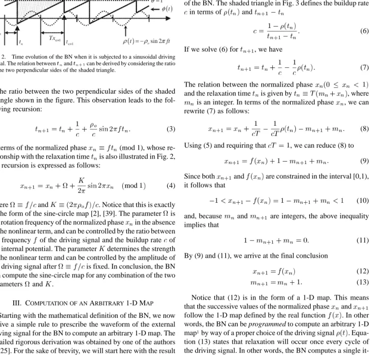
Fig. 2. Time evolution of the BN when it is subjected to a sinusoidal driving signal. The relation betweent and t can be derived by considering the ratio of the two perpendicular sides of the shaded triangle.
is the ratio between the two perpendicular sides of the shaded triangle shown in the figure. This observation leads to the fol-lowing recursion:
(3) In terms of the normalized phase (mod 1), whose re-lationship with the relaxation time is also illustrated in Fig. 2, the recursion is expressed as follows:
mod (4) where and . Notice that this is exactly in the form of the sine-circle map [2], [39]. The parameter is the rotation frequency of the normalized phase in the absence of the nonlinear term, and can be controlled by the ratio between the frequency of the driving signal and the buildup rate of the internal potential. The parameter determines the strength of the nonlinear term and can be controlled by the amplitude of the driving signal after is fixed. In conclusion, the BN can compute the sine-circle map for any combination of the two parameters and .
III. COMPUTATION OF ANARBITRARY1-D MAP
Starting with the mathematical definition of the BN, we now derive a simple rule to prescribe the waveform of the external driving signal for the BN to compute an arbitrary 1-D map. The detailed rigorous derivation was obtained by one of the authors in [25]. For the sake of brevity, we will start here with the result and focus on its proof.
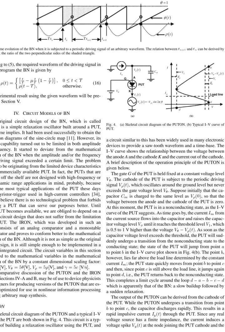
Fig. 3 shows the time evolution of the BN when it is sub-jected to a periodic driving signal of an arbitrary waveform. The driving signal is periodic but is piecewise continuous, i.e., it has periodic jumps, or discontinuities in mathematical terms, during every cycle. The following equation defines the driving signal:
otherwise (5) where is the period of the modulation signal and the func-tion is a real function defined on the unit interval,
. The first case in (5) defines the driving signal for a single period, while the second case completes the defini-tion by making it periodic with period .
Given the driving signal and the buildup rate of the in-ternal potential, the relation between successive relaxation times can be derived as follows. Let be the time of -th relaxation
of the BN. The shaded triangle in Fig. 3 defines the buildup rate in terms of and
(6) If we solve (6) for , we have
(7) The relation between the normalized phase
and the relaxation time is given by , where is an integer. In terms of the normalized phase , we can rewrite (7) as follows:
(8) Using (5) and requiring that , we can reduce (8) to
(9) Since both and are constrained in the interval [0,1), it follows that
(10) and, because and are integers, the above inequality implies that
(11) By (9) and (11), we arrive at the final conclusion
(12) (13) Notice that (12) is in the form of a 1-D map. This means that the successive values of the normalized phase and follow the 1-D map defined by the real function . In other words, the BN can be programmed to compute an arbitrary 1-D map1by way of a proper choice of the driving signal .
Equa-tion (13) states that relaxaEqua-tion will occur once every cycle of the driving signal. In other words, the BN computes a single it-eration of a 1-D map at every cycle of the driving signal. This is particularly important when we need to have many identical maps working together. In a network of 1-D maps, the common external driving signal will act as a central clock that coordi-nates the synchronous stepping of all the maps.
As an example, suppose we want to program the BN to com-pute the logistic map. The recursion of the logistic map is given by
(14) A comparison with (12) produces the expression for
(15)
1Because the functionf(x) is defined on the unit interval, the 1-D maps that
the BN can compute will be restricted to those defined on the unit interval. How-ever, this does not result in a serious limitation of the BN since many 1-D maps are actually defined on the unit interval, while most others can be transformed to one on the unit interval by a suitable scaling of a variable.
Fig. 3. Time evolution of the BN when it is subjected to a periodic driving signal of an arbitrary waveform. The relation betweent andt can be derived by considering the ratio of the two perpendicular sides of the shaded triangle.
According to (5), the required waveform of the driving signal in order to program the BN is given by
otherwise. (16) The experimental result using the given waveform will be pre-sented in Section V.
IV. CIRCUITMODELS OFBN
The original circuit design of the BN, which is called PUTON, is a simple relaxation oscillator built around a PUT, as the name implies. It had been used successfully to obtain the bifurcation diagrams of the sine-circle map [11]. However, its dynamic capability turned out to be limited in both amplitude and frequency. It started to deviate from the mathematical definition of the BN when the amplitude and/or the frequency of the driving signal exceeded a certain limit. The problem seemed to be originating from the limited device characteristics of the commercially available PUT. In fact, the PUTs that are available off the shelf are not designed with high-frequency or wide-dynamic range applications in mind, probably, because one of the most typical applications of the PUT these days is the thyristor-trigger used in high-current controllers [34], [35]. We believe there is no technological problem that forbids designing a PUT that can serve our purposes better. Until such a PUT becomes available, we are obliged to depend on a different circuit design that does not suffer from the limitation of the PUT. The IRON, which was developed in such an effort, consists of an analog comparator and a monostable multivibrator and proves to conform better to the mathematical definition of the BN. Although it is not as simple as the original circuit design, it is still simple enough to be implemented in a compact integrated circuit. The circuit variables in this section are related to the mathematical variables in the mathematical definition of the BN by a constant dimensional scaling factor:
V , V , V , and V/s . The comparative discussion of the PUTON and the IRON given in Sections IV-A and B, may be of use to device physicists and designers for producing versions of the PUTON that are es-pecially optimized for use in nonlinear information processing including arbitrary map synthesis.
A. PUTON
The skeletal circuit diagram of the PUTON and a typical I–V curve of the PUT are both shown in Fig. 4. This circuit is a typ-ical way of building a relaxation oscillator using the PUT, and
Fig. 4. (a) Skeletal circuit diagram of the PUTON. (b) Typical I–V curve of PUT.
a circuit similar to this has been widely used in many electronic devices to provide a saw-tooth waveform and a time-base. The I–V curve shows the relationship between the voltage between the anode A and the cathode K and the current out of the cathode. A brief description of the operation principle of the PUTON is given below.
The gate G of the PUT is held fixed at a constant voltage level . The cathode of the PUT is subject to the periodic driving signal , which oscillates around the ground level but never exceeds the gate voltage level . Suppose initially that the ca-pacitor is charged to the same level as , so that the voltage between the anode and the cathode of the PUT is zero. At this moment, the PUT is in a nonconducting state, as the I–V curve of the PUT suggests. As time goes by, the current from the current source flows into the capacitor and raises the capac-itor voltage level until it reaches the threshold level , which is 0.5 to 1 V higher than the voltage . As soon as the capacitor voltage level exceeds the threshold, the PUT will sud-denly undergo a transition from the nonconducting state to the conducting state; the state of the PUT will jump from point to point in the I–V curve plot shown in Fig. 4(b). The point , however, lies far above the load line determined by the constant current ; the PUT state quickly moves from point to point and then, since point is still above the load line, it jumps again to point , i.e., the PUT returns back to the nonconducting state. This completes a limit cycle around the loop
which is apparently that of the BN: a slow buildup followed by a sudden relaxation.
The output of the PUTON can be derived from the cathode of the PUT. While the PUTON undergoes a transition from point to point , the capacitor discharges rapidly. This results in a rapid impulsive current through the PUT. Since any real voltage source has a finite impedance, the current induces a voltage spike at the node joining the PUT cathode and the
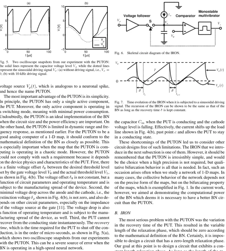
Fig. 5. Two oscilloscope snapshots from our experiment with the PUTON: the solid lines represent the capacitor voltage levelV while the dotted lines represent the sinusoidal driving signalV : (a) without driving signal, i.e., V =
0; (b) with 10-kHz driving signal.
voltage source , which is analogous to a neuronal spike, and hence the name PUTON.
The most important advantage of the PUTON is its simplicity. In principle, the PUTON has only a single active component, the PUT. Moreover, the only active component is operating in a switching mode, meaning with minimal power consumption. Undoubtedly, the PUTON is an ideal implementation of the BN when the circuit size and the power efficiency are important. On the other hand, the PUTON is limited in dynamic range and fre-quency response, as mentioned earlier. For the PUTON to be a good analog computer of a 1-D map, it should conform to the mathematical definition of the BN as closely as possible. This is especially important when the map that the PUTON is com-puting is operating in a chaotic mode. However, the PUTON could not comply with such a requirement because it depends on the device physics and characteristics of the PUT. First, there is a finite voltage offset between the desired threshold level set by the gate voltage level and the actual threshold level , as shown in Fig. 4(b). The voltage offset is not constant, but a function of circuit parameters and operating temperature and is subject to the manufacturing spread of the device. Second, the minimal voltage drop across the anode and the cathode, i.e., the extinction voltage shown in Fig. 4(b), is not zero, and also de-pends on other circuit parameters, especially on the impedance of the voltage source at the gate [11]. The voltage drop is also a function of operating temperature and is subject to the manu-facturing spread of the device, as well. Third, the PUT cannot recover from the conducting state instantaneously. The recovery
time, which is the time required for the PUT to shut off the
con-duction, is in the order of micro-seconds, as shown in Fig. 5(a), which shows two oscilloscope snapshots from our experiments with the PUTON. This can be a severe source of error when the BN is operating in a high-speed neural network.
The last problem was the most critical factor that forced us to look for other implementation possibilities. If only the recovery time were constant, the problem could be handled easily; we could lower the threshold level slightly to reduce the length of the buildup phase by the amount that can offset the error due to the recovery time. The recovery time, however, varies appre-ciately with the worst case occurring when the driving signal is falling rapidly: the PUT simply cannot be turned off. This phenomenon, that we call sliding of the PUTON, is exempli-fied in Fig. 5(b). A closer examination of the circuit revealed that the sliding of the PUTON is due to the current supplied by
Fig. 6. Skeletal circuit diagram of the IRON.
Fig. 7. Time evolution of the IRON when it is subjected to a sinusoidal driving signal. The recursion of the IRON can be shown to be the same as that of the BN as long as the recovery time is kept constant.
the capacitor when the PUT is conducting and the cathode voltage level is falling. Effectively, the current shifts up the load line shown in Fig. 4(b), past point and allows the PUT to stay in a conducting state.
These shortcomings of the PUTON led us to consider other circuit designs free of such limitations. The IRON that we intro-duce in the next subsection is one of them. However, it should be remembered that the PUTON is irresistibly simple, and would be the choice when a high precision is not required, but quali-tative bifurcation behavior is all that is needed. In fact, such an occasion arises often when we study a network of 1-D maps. In many cases, the collective behavior of the network depends not on the precise form of the maps, but on the bifurcating property of the maps, which is exemplified in Fig. 1. In the current work, however, we aimed at demonstrating the computational power of the BN which deems it is necessary to have a better BN cir-cuit than the PUTON.
B. IRON
The most serious problem with the PUTON was the variation in the recovery time of the PUT. This resulted in the variable length of the relaxation phase, which should be zero according to the mathematical definition of the BN. Certainly, it is impos-sible to design a circuit that has a zero-length relaxation phase. Our goal at this point is to design a circuit that exhibits a con-stant-length relaxation phase. As long as the length of the re-laxation phase is kept constant, it can be compensated by other circuit parameters.
Fig. 6 shows a simplified circuit diagram of the IRON. When the switch S is open, the current from the current source charges the capacitor until the voltage level reaches the threshold voltage . As soon as the capacitor voltage exceeds the threshold voltage , the output of the comparator jumps and triggers the monostable multivibrator. The output of the monostable multivibrator then turns on the switch and causes the capacitor to discharge until its level reaches the modulation
Fig. 8. Actual circuit diagram of the IRON. The waveforms at the four probe points are shown in Fig. 9.
voltage level . Apparently, we now have a constant recovery time as long as the pulse width of the monostable multivibrator is constant. One may argue that the recovery time still cannot be constant in a strict sense because it will be now dependent on the characteristics of the monostable multivibrator. This is true, but now the problem of constant recovery time is separated from the threshold dynamics and in a much more manageable form. A well-designed monostable multivibrator can keep the variability of the pulse width within 1%, if it is operating in a reasonable condition [40].
Fig. 7 illustrates how the constant nonzero recovery time can be compensated by shifting other circuit parameters. By the same argument that led us to (12), we can express the constant buildup rate , analogous to in (6) as follows:
(17) The recursion that relates the successive relaxation times of the IRON is found then to be
(18) The constant offset can be absorbed in the time variable if we insert a pause of the same amount before every cycle of the driving signal, i.e., by substituting for in (18), we have
(19) This is now in the same general format of (7). The additive term in the parameter of the function can be canceled out if we insert a constant pause of amount before every cycle of the driving signal since, as we have shown in Section III, firing occurs exactly once every cycle of the driving signal.
Fig. 8 shows the actual circuit diagram of the IRON. The two bold faced amplifier symbols represent voltage followers. Around the capacitor C1 there is a current source using a bipolar transistor, a JFET switch controlling the path from the input buffer to the capacitor, and an analog comparator (LM311). The resister R9 can be trimmed to control the constant current flowing into the capacitor. The two transistors near the switch are added simply to shift the voltage level of the control signal
Fig. 9. SPICE simulation result of the IRON: the four curves show the waveforms at the four probe points marked in Fig. 8.
VC, which is derived from the collectors of Q4 and Q5, to a level suitable to control the JFET switch. The part after the com-parator corresponds to the monostable multivibrator in Fig. 6. The two symmetrically located transistors Q4 and Q5 form a
NANDgate, and the third transistor Q6 is acting as an inverter. The output of the inverter is fed back to theNANDgate via a ca-pacitor coupling. The net result is that we have a pulse of a con-stant width whenever the output of the comparator goes high. Fig. 9 shows a SPICE [41] simulation result of the circuit. The four curves show the waveforms at the four probe points marked in Fig. 8. Note that the pulse width, which corresponds to the re-covery time, is now constant.
Another advantage of the IRON over the PUTON is that it is providing well-formed output pulses as shown in Fig. 9. In the PUTON, output pulses can be derived from the cathode of the PUT. However, they are not uniform in amplitude and, more-over, are superimposed on the driving signal. Separating them from the driving signal and reshaping them will require extra cir-cuit complexity. In addition, the PUTON will eventually require the voltage followers, like the IRON does, to isolate it from the external circuitry. Taking all these factors into account, we can say that the circuit complexity of the IRON does not greatly ex-ceed that of the PUTON. Considering the number of transistors needed for the comparator, the complexity of the IRON is about half that of the classic timer chip 555 [42], the classic timer chip, which has long been used in a compact integrated circuit.
V. EXPERIMENTALRESULTS
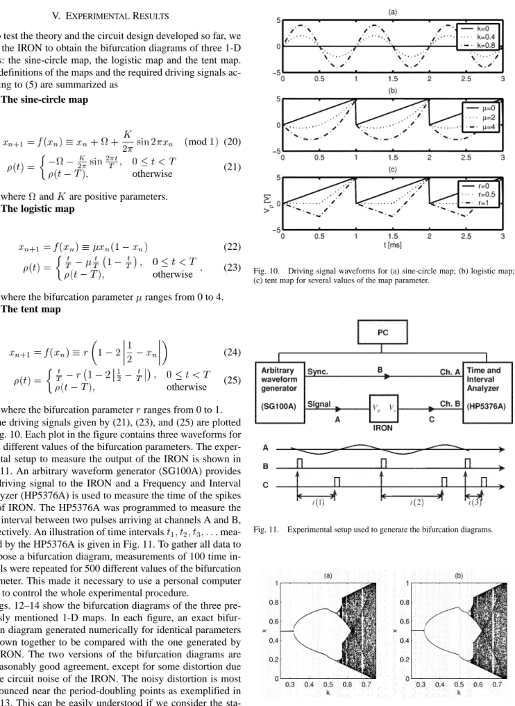
To test the theory and the circuit design developed so far, we used the IRON to obtain the bifurcation diagrams of three 1-D maps: the sine-circle map, the logistic map and the tent map. The definitions of the maps and the required driving signals ac-cording to (5) are summarized as
The sine-circle map
mod (20) otherwise (21) where and are positive parameters.
The logistic map
(22) otherwise (23) where the bifurcation parameter ranges from 0 to 4.
The tent map
(24) otherwise (25) where the bifurcation parameter ranges from 0 to 1. The driving signals given by (21), (23), and (25) are plotted in Fig. 10. Each plot in the figure contains three waveforms for three different values of the bifurcation parameters. The exper-imental setup to measure the output of the IRON is shown in Fig. 11. An arbitrary waveform generator (SG100A) provides the driving signal to the IRON and a Frequency and Interval Analyzer (HP5376A) is used to measure the time of the spikes out of IRON. The HP5376A was programmed to measure the time interval between two pulses arriving at channels A and B, respectively. An illustration of time intervals mea-sured by the HP5376A is given in Fig. 11. To gather all data to compose a bifurcation diagram, measurements of 100 time in-tervals were repeated for 500 different values of the bifurcation parameter. This made it necessary to use a personal computer (PC) to control the whole experimental procedure.
Figs. 12–14 show the bifurcation diagrams of the three pre-viously mentioned 1-D maps. In each figure, an exact bifur-cation diagram generated numerically for identical parameters is shown together to be compared with the one generated by the IRON. The two versions of the bifurcation diagrams are in reasonably good agreement, except for some distortion due to the circuit noise of the IRON. The noisy distortion is most pronounced near the period-doubling points as exemplified in Fig. 13. This can be easily understood if we consider the sta-bility of the 1-D map; the system is marginally stable near the period-doubling points and will accumulate the circuit noise
Fig. 10. Driving signal waveforms for (a) sine-circle map; (b) logistic map; (c) tent map for several values of the map parameter.
Fig. 11. Experimental setup used to generate the bifurcation diagrams.
Fig. 12. Bifurcation diagrams of the sine-circle map: (a) by an actual measurement of the output of the IRON; (b) by a numerical computation.
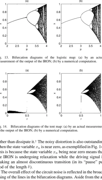
Fig. 13. Bifurcation diagrams of the logistic map: (a) by an actual measurement of the output of the IRON; (b) by a numerical computation.
Fig. 14. Bifurcation diagrams of the tent map: (a) by an actual measurement of the output of the IRON; (b) by a numerical computation.
rather than dissipate it.2The noisy distortion is also outstanding
when the state variable is near zero, as exemplified in Fig. 14. This is because the state variable being near zero means that the IRON is undergoing relaxation while the driving signal is making an almost discontinuous transition (in its “pause” pe-riod of the length ).
The overall effect of the circuit noise is reflected in the broad-ening of the lines in the bifurcation diagrams. Aside from the ac line noise, which was difficult to avoid due to the single-ended nature of the input and output ports of the measurement equip-ments, the most outstanding source of noise was found in the arbitrary waveform generator. We are not sure whether the noise is the quantization noise of the digital-to-analog converter or is originating from the coupling between the analog and the dig-ital parts of the waveform generator. The effect of the noise from the arbitrary waveform generator can be well appreciated if we compare the bifurcation diagram in Fig. 12(a) with other two diagrams in Figs. (13a) and (14a). Because the driving signal required to compute the sine-circle map is simply a sinusoidal wave, we could use a function generator (HP3325B) in place of an arbitrary waveform generator in the experiment to compute the bifurcation diagram Fig. 12(a). Apparently, the bifurcation diagram in Fig. 12(a) looks much cleaner than the other two diagrams.
To evaluate the IRON in the absence of such noise sources we used PSPICE [41] to simulate the IRON and generate the bifurcation diagrams. This showed that the resulting bifurcation diagrams were as clean as the numerical versions. Although one
2When the logistic map is near the period-doubling bifurcation points, it can
be shown thatj(dx )=(dx )j = 1, where k = 1 for the first bifurcation,
k = 2 for the second bifurcation, and so on. This means the logistic map is
marginally stable near the period-doubling bifurcation points.
cannot expect complete freedom from noise sources in a real circuit, we expect that we can reduce the effect of noise to a negligible degree when such noise sources are properly coped with, and especially when the IRON is transported onto a printed circuit board, or eventually to a VLSI chip.
VI. CONCLUSION
Starting from the fact that the BN can compute the sine-circle map when it is subject to a sinusoidal driving signal, we gener-alized the BN and showed that the computational power of the BN can be extended to compute an arbitrary 1-D map such as the logistic map or the tent map. The programming of the BN to compute an arbitrary map was possible simply by changing the waveform of the driving signal. We described two circuit models of the BN: the PUTON and the IRON. We used the IRON to generate the bifurcation diagrams of the sine-circle map, the lo-gistic map and the tent map, and could see that they were in good agreement with those generated numerically.
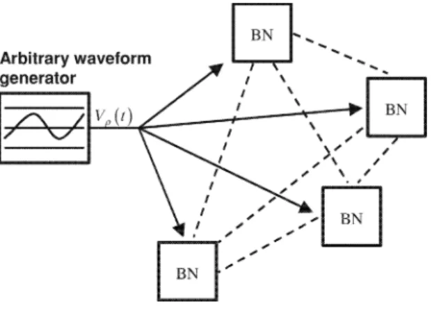
Among other features in which we are most interested is the
programmability of the BN. Fig. 15 shows a typical situation
when many BNs are combined to form a network. A waveform generator is used to provide a common driving signal to all BNs. In the absence of the driving signal, the BNs by themselves are mere relaxation oscillators. Most likely, they will be firing ran-domly and, at best, they will be able to reach a global synchro-nization. With the introduction of the driving signal, the network suddenly becomes a coupled map lattice, e.g., consisting of lo-gistic maps. It will start to exhibit various patterns of spatio-temporal chaos depending critically on the amplitude of the driving signal and the type of coupling between BNs. The next moment that the driving signal is switched to something else, the network then turns into a different coupled map lattice, e.g., consisting of sine-circle maps. Possibly, it will now be able to exhibit soliton turbulence [24].
Before concluding, we feel it is necessary to comment on pos-sible ways to achieve coupling among the BNs. Without doubt, the practical value of the BN will be heavily dependent on the availability of an efficient coupling method. A straightforward way would start with a step to derive an analog voltage propor-tional to the normalized phase from the output of the BN. This can be done easily, e.g., by sample-and-holding the voltage level of a saw-tooth waveform, which can be shared among the BNs, at the moment a BN fires. Once such a voltage output is available, it can be used to advance or delay the firing time of a target BN, e.g., by using it to control the threshold level or the slope of the buildup of the internal potential of the target BN. Although this coupling method requires a substantial cir-cuit complexity compared with the other methods that we will mention below, it is flexible enough to realize such a complex type of coupling, as is required by the parametrically coupled map lattice (PCML) [26]–[29]. Another way of coupling would be to establish resistive links among the capacitors of the BNs and activate the links periodically at the end of every cycle of the periodic driving signal. This would be the most natural way to achieve a diffusive coupling as is required by the Coupled Map Lattice [16], [24]. Yet another way of coupling is pulse-coupling among the BNs. An impulse from a source BN can be applied to a target BN directly to affect its threshold level or the internal
Fig. 15. Network of the BNs sharing the same driving signal. The dotted lines represent coupling between the BNs.
potential . Although this type of coupling method is rather re-strictive in terms of the possible types of coupling it can realize, we are most interested in it because it is a natural and straightfor-ward way to take full advantage of the biomorphic nature of the BN. We are currently investigating actively the associative dy-namics and chaotic annealing dydy-namics of a BN network, which is utilizing a pulse-coupling method.
Finally, a new literature search for relevant papers that may have appeared in the interim was deemed necessary and carried out. This, together with reviewers’ comments, brought to our attention several papers related to this work. These have been added to the list of references [43]–[47]. Careful examination of the chronology of this body of work and that in our past work, [8]–[11], [25], [37], shows that the concept of arbitrary map synthesis described here was arrived at independently. The first observations in our work leading to the idea of modifying the bifurcation diagram of a driven spiking oscillator, by altering the waveform of the periodic driving signal, were made in 1997 [37] and pursued further in [25]. The concept of arbitrary map synthesis described here was arrived at therefore independently and in a distinctly different manner and emphasis than that described in Saito and coworkers work [43]–[45]. The CMOS circuit for generating arbitrary maps described in [46] employs pulse-width modulation rather than alteration of the driving signal waveform described here. It is worth noting that the quality of the measured bifurcation diagrams in our work (Figs. 12–14) surpass those given in [46]. This suggests that the waveform control method presented here may have advantages over other techniques especially when a VLSI version of the circuit in Fig. 8 is realized with proper attention given for dealing with discontinuities as was outlined earlier.
REFERENCES
[1] R. M. May, “Simple mathematical models with very complicated dy-namics,” Nature, vol. 26, pp. 459–467, 1976.
[2] R. Perez and L. Glass, “Bistability period-doubling bifurcation and chaos in periodically forced oscillator,” Phys. Lett. A, vol. 90, pp. 441–443, 1982.
[3] M. H. Jensen, P. Bak, and R. Bohr, “Transition to chaos by interaction of resonances in dissipative systems. I. Circle maps,” Phys. Rev. A, vol. 30, pp. 1960–1969, 1984.
[4] R. Bohr, P. Bak, and M. H. Jensen, “Transition to chaos by interaction of resonances in dissipative systems. II. Josephson junctions, charge-den-sity waves, and standard maps,” Phys. Rev. A, vol. 30, pp. 1970–1981, 1984.
[5] A. S. Pikovsky, “A dynamical model for periodic and chaotic oscillations in the Belousov-Zhabotinsky reaction,” Phys. Lett. A, vol. 85, no. 1, pp. 13–16, 1981.
[6] R. H. Simoyi, A. Wolf, and H. L. Swinney, “One-dimensional dynamics in a multicomponent chemical reaction,” Phys. Rev. Lett., vol. 49, no. 4, pp. 245–248, 1982.
[7] F. Papoff, A. Fioretti, and E. Arimondo, “Return maps for intensity and time in a homoclinic-chaos model applied to a laser with a saturable absorber,” Phys. Rev. A, vol. 44, no. 7, pp. 4639–4651, 1991. [8] N. H. Farhat and M. Eldefrawy, “The bifurcating neuron,” in Dig. Ann.
OSA Meeting, San Jose, CA, 1991, pp. 10–10.
[9] , “The bifurcating neuron: characterization and dynamics,” in Pho-tonics for Computers, Neural Networks, and Memories. San Diego, CA: SPIE, July 1992, vol. 1773, pp. 23–34.
[10] N. H. Farhat, S.-Y. Lin, and M. Eldefrawy, “Complexity and chaotic dynamics in a spiking neuron embodiment,” in Adaptive Computing: Mathematics, Electronics, and Optics. Orlando, FL: Society of Photo-Optical Instrumentation Engineers, Apr. 1994, vol. 55, pp. 77–88. [11] S.-Y. Lin, “Synchronicity and coherence in artificial neural networks,”
Ph.D.dissertation, Elect. Eng. Dep.,Univ. Pennsylvania, Philadelphia, 1994.
[12] M. Zeller, M. Bauer, and W. Martienssen, “Neural dynamics modeled by one-dimensional circle maps,” Chaos, Solitons, Fractals, vol. 5, no. 6, pp. 885–893, 1995.
[13] P. A. Anninos, B. Beek, T. J. Csermely, E. M. Harth, and G. Pertile, “Dynamics of neural structures,” J. Theor. Biol., vol. 26, pp. 121–148, 1970.
[14] E. Harth, “Order and chaos in neural systems: an approach to the dy-namics of higher brain functions,” IEEE Trans. Syst., Man, Cybern., vol. SMC-13, no. 5, pp. 782–789, 1983.
[15] M. Usher, H. G. Schuster, and E. Niebur, “Dynamics of populations of integrated-and-fire neurons, partial synchronization and memory,” Neural Computation, vol. 5, pp. 570–586, 1993.
[16] K. Kaneko, “Overview of coupled map lattices,” Chaos, vol. 2, no. 3, pp. 279–282, 1992.
[17] H. Nozawa, “A neural network model as a globally coupled map and applications based on chaos,” Chaos, vol. 2, no. 3, pp. 377–386, 1992. [18] M. Inoue and A. Nagayoshi, “A chaos neuro-computer,” Phys. Rev. A,
vol. 158, pp. 373–376, 1991.
[19] C. B. Price, P. Wambacq, and A. Oosterlinck, “The plastic coupled map lattice: a novel image-processing paradigm,” Chaos, vol. 2, no. 3, pp. 351–366, 1992.
[20] A. V. Oppenheim, G. W. Wornell, S. H. Isabelle, and K. M. Cuomo, “Signal processing in the context of chaotic signals,” in Proc. IEEE Int. Conf. Acoustics, Speech, Signal Processing, vol. 4, 1992, pp. 117–120. [21] G. Heidari-Bateni and C. D. McGillem, “A chaotic direct-sequence spread-spectrum communication system,” IEEE Trans. Commun., vol. 42, pp. 1524–1527, Feb. 1994.
[22] B. Chen and G. W. Wornell, “Efficient channel coding for analog sources using chaotic systems,” in Proc. IEEE Global Telecommunica-tions Conf., Nov., 18–22 1996, vol. 1, pp. 131–135.
[23] G. Hu, J. Xiao, J. Yang, F. Xie, and Z. Qu, “Synchronization of spa-tiotemporal chaos and its applications,” Phys. Rev. E, vol. 56, no. 3, pp. 2738–2746, 1997.
[24] K. Kaneko, Theory and Applications of Coupled Map Lat-tices. Chichester, U.K.: Wiley, 1993.
[25] E. Del Moral Hernandez, “Artificial neural networks based on bifur-cating recursive processing elements,” Ph.D. dissertation, Elect. Eng. Dep., Univ. Pennsylvania, Philadelphia, 1998.
[26] N. H. Farhat and E. Del Moral Hernandez, “Logistic networks with DNA-like encoding and interactions,” in Lecture Notes in Computer Sci-ence. Berlin, Germany: Springer-Verlag, 1995, vol. 930, pp. 214–222. [27] , “Recurrent networks with recursive processing elements: a para-digm for dynamical computing,” in Proc. SPIE , vol. 2824, Denver, CO, 1996, pp. 158–170.
[28] N. H. Farhat, E. D. M. Hernandez, and G. Lee, “Strategies for au-tonomous adaptation and learning in dynamical networks,” in Proc. Int. Work Conf. Artificial Natural Neural Networks, Lanzarote, Spain, 1997. [29] N. Farhat, G. Lee, and X. Ling, “Dynamical networks for ATR,” in Proc. RTO Meeting 6: Non-Cooperative Air Target Identification Using Radar, Nov. 1998, pp. D-1–D-9.
[30] N. H. Farhat and M. Eldefrawy, “Complexity and chaotic dynamics in a photonic neuron embodiment,” in Proc. 1st Symp. Nonlinear Theory Applications, vol. 1, Dec. 1993, pp. 91–97.
[31] A. V. Holden and S. M. Ramadan, “The response of a molluscan neuron to a cyclic input: entrainment and phase-locking,” Biol. Cybern., vol. 41, pp. 157–163, 1981.
[32] A. V. Holden, W. Winlow, and P. G. Haydon, “The induction of periodic and chaotic activity in a molluscan neuron,” Biol. Cybern., vol. 43, pp. 169–173, 1982.
[33] K. Aihara and G. Matsumoto, “Chaotic oscillations and bifurcations in squid giant axons,” in Chaos, A. V. Holden, Ed: Princeton University Press, 1986, pp. 257–269.
[34] S. M. Sze, Physics of Semiconductor Devices, 2nd ed. New York: Wiley, 1981.
[35] R. K. Sugandhi, Thyristors, Theory and Applications, 2nd ed. New York: Wiley, 1984.
[36] L. Trajkovic and J. A. N. Willson, “Complementary two-transistor cir-cuits and negative differential resistance,” IEEE Trans. Circir-cuits Syst., vol. 37, pp. 1258–1265, 1990.
[37] A. S. Baek, “Pulse-Coupled networks: dynamics, applications, and im-plementations,” Ph.D. dissertation, Elect. Eng. Dep.,Univ. Pennsylvania, Philadelphia, 1997.
[38] M. P. Kennedy and L. O. Chua, “van der pol and chaos,” IEEE Trans. Circuits Syst., vol. 44, pp. 974–980, 1997.
[39] R. C. Hilborn, Chaos and Nonlinear Dynamics, An Introduction for Sci-entists and Engineers. New York: Oxford Univ. Press, 1994. [40] AN-372: Application Note 372 Designer’s Encyclopedia of Bipolar
One-Shots, F. S. Corporation. (1998, Apr.). [Online]. Available: http://www.fairchildsemi.com
[41] MicroSim, MicroSim PSpice and Basics: User’s Guide, MicroSim Corp., San Jose, CA, 1997.
[42] LM555/LM555C Timer, N. S. Corporation. (1997, May). [Online]. Available: http://www.national.com
[43] H. Torikai and T. Saito, “A multiplex communication system using chaotic pulse-train with sawtooth control,” in Proc. IEEE Int. Symp. Circuits Systems, vol. 2, 1997, pp. 1065–1068.
[44] , “Return map quantization from an integrate-and-fire model with two periodic inputs,” IEICE Trans. Fund., vol. E82-A, no. 7, pp. 1336–1343, 1999.
[45] , “Resonance phenomenon of interspike intervals from an inte-grate-and-fire model with two periodic inputs,” IEEE Trans. Circuits Syst. I, vol. 48, pp. 1198–1204, Oct. 2001.
[46] T. Moire, S. Sakbayashi, M. Nagata, and A. Iwaty, “Cmos circuits gen-erating arbitrary chaos by using pulse-width modulation techniques,” IEEE Trans. Circuits Syst. I, vol. 47, pp. 1652–1657, Nov. 2000. [47] M. Delgado-Restito and A. Rodriquez-Vazquez, “Integrated chaos
gen-erator,” Proc. IEEE, vol. 90, pp. 747–767, May 2002.
[48] N. H. Farhat and M. Eldefrawy, Proc. Int. Symp. on Nonlinear Theory and Applications, vol. 1, Dec. 1993, pp. 91–97.
Emilio Del Moral Hernandez (S’90–M’99) received the B.Sc and M.Sc
de-grees in electrical engineering from the Polytechnic School of the University of Sao Paulo, Sao Paulo, Brazil, and the Ph.D. degree in electrical engineering from the University of Pennsylvania, Philadelphia.
He is currently with the Department of Electronic Systems Engineering, Uni-versity of Sao Paulo, where he teaches topics in electrical measurements and data acquisition systems, design of electronic circuits (analog and digital), dig-ital filters design and modeling in signal processing, fundamentals of artifi-cial neural networks, nonlinear dynamics and bifurcation phenomena applied to neural networks. His research activities include the fields of computational intelligence, neuro-like computation and biologically inspired information pro-cessing, complex systems and nonlinear dynamics, modeling of nonlinear mag-netic materials, pattern recognition, classification and clustering, data mining, digital signal processing, optimization, the development of novel neurocom-puting architectures which explore bifurcation and chaos, hybrid architectures which blend more than one classical neural architecture, and data fusion and multisensors systems for environmental and medical applications.
Dr. Del Moral Hernandez is a member of IEEE Circuits and Systems Society and the IEEE Neural Networks Society.
Geehyuk Lee received the M.Sc. degree in physics from the Korean Advanced
Institute of Science and Technology, Daejeon, South Korea, in 1992 and the Ph.D. degree in electrical engineering from the University of Pennsylvania, Philadelphia, in 2000.
Since 2002, he is an Assistant Professor at the Information and Communica-tions University, Daejeon, South Korea. His scientific interest as a Ph.D. student was in the field of collective behavior of pulse-coupled spiking neurons, and in his thesis he proposed two types of bifurcating neuron networks in an effort to elucidate the possible roles and potentials of chaos and synchrony in the neural network. His current research interests are in the application of artificial neural networks and other machine learning algorithms to human-computer interaction devices and smart home environments.
Nabil H. Farhat (S’58–M’63–SM’72–F’81–LF’99) received the B.Sc. degree
from the Technion, Haifa, Israel, in 1957, the M.Sc. degree from the University of Tennessee, Knoxville, in 1959, and the Ph.D. degree from the University of Pennsylvania, Philadelphia, in 1963, all in electrical engineering.
In 1964, he joined the Faculty of the Moore School of Electrical Engineering, University of Pennsylvania, where he is now Professor of Electrical Engineering and heads the Electro-Optics and Photonic Neuroengineering Laboratory. His current research interests are in collective nonlinear dynamical information processing, neural networks, photonic realization of neurocomputers, and Corticonics where he is applying concepts and tools from nonlinear dynamics, bifurcation theory, information driven self-organization and chaos to the modeling and study of cortical information processing. His teaching includes courses in EM theory, electro-optics, electron and light optics, holography and neurodynamics and neural networks on both graduate and undergraduate levels. His past research included microwave imaging, holography, automated target recognition, optical information processing and the study of the interaction of EM radiation with plasmas and solids in the context of millimeter wave and laser output energy measurement with glow discharge plasmas.
While Associate Professor, Dr. Farhat was named to the Ennis Chair in Elec-trical Engineering. He has served as Distinguished Visiting Scientist at the Jet Propulsion Laboratory, Pasadena, CA. He is a recipient of the University of Pennsylvania Christian R. and Mary F. Lindback Foundation Award for dis-tinguished teaching. He is a Fellow of the Optical Society of America, and is Member of Sigma Xi, Eta Kappa Nu, the Electromagnetics Academy, and the American Institute of Physics. He has also served on the National Board of Di-rectors of Eta Kappa Nu, RCA consultant, and as the Editor of Advances in Holography, an Associate Editor of Acoustical Imaging and Holography, an Action Editor of Neural Computation, and an Advisory Editor of Optics Let-ters. He is presently an Action Editor for Neural Networks.