Multi-port Current Source Inverter for Smart
Microgrid Applications: A Cyber Physical Paradigm
Karthikrajan Senthilnathan1‡ , and K.Iyswarya Annapoorani2,‡ *
1 Vellore Institute of Technology, Chennai, India; [email protected] 2 Vellore Institute of Technology, Chennai, India; [email protected]
* Correspondence: [email protected]
‡ Conceptualization, Karthikrajan Senthilnathan and K Iyswarya Annapoorani; Methodology, Karthikrajan Senthilnathan and K Iyswarya Annapoorani; Supervision, K Iyswarya Annapoorani..
1
2
3
4
5
6
7
8
9
Abstract:Thispaperpresentsaconfigurationofdualoutputsinglephasecurrentsourceinverterwith 6switchesformicrogridapplications.Theinverteriscapableofdeliveringpowertotwoindependent setofloadsofequalvoltagesordifferentvoltagesattheloadend.Thecontrolstrategyisbasedon IntegralSlidingModeControl(ISMC).Theremotemonitoringoftheinverterisperformedwithcyber infrastructure.ThecyberphysicaltestbenchisdevelopedbasedonReconfigurableI/Oprocessor (NIMyRIO-1900)for controlandmonitoringoftheinverter. Theinverterprototype istestedin cyberphysicaltestbenchin laboratoryconditions. Theperformanceofthe inverterisanalyzed andmonitoredthroughtheremotesystem. Also,theinverterisanalyzedwithdifferentvoltage conditions.
Keywords:Cyberphysicalsystems;Dualoutputinverter;Rapidcontrolprototype. 10
1. Introduction 11
The distributed generation (DG) with photo voltaic, wind energy, fuel cell, and battery termed 12
as microgrid which is able to supply for low and medium voltage applications. The DC microgrid is 13
capable of supplying both DC loads and AC loads with inverter. The inverters for microgrid discussed 14
in [1], [2] are capable of supplying single output. The inverters with reduced semiconductor switches 15
and dual output is capable of feeding dual loads and less complexity in implementation. This enables 16
the feeding of different types of loads using an inverter. The development of inverter with reduced 17
power semiconductor devices make the system economical and compact. The dual output inverters 18
reduces the number of switches in a system and supplies energy to two AC autonomous loads. Four 19
switch inverter [3] is initially proposed with reduced number of switches by replacing split capacitors 20
for sharing between power converters. The dual output voltage source inverters discussed by Yu, 21
Strake et.al [4] are dual phase single DC bus inverter with four switches, three wire single phase 22
inverter with six switches, dual phase dual DC bus inverter with four switch, dual phase with four 23
switch and transformer. The inverter models discussed in [4] has the capability of operating only in 24
half bridge configuration. The dual output single phase inverter based on voltage source inverters 25
(VSI) is proposed by Fatemi, e.al. [5] explains about the half bridge dual output inverter with split 26
capacitor as a sharing leg for both outputs and for the full bridge dual output with six switches, the 27
switch leg is common of for both outputs by sharing a row of switches for upper and lower outputs. 28
The six switch voltage source inverter delivers equal voltage at output with open loop operation. The 29
six switch dual output with buck structure delivers dual output with equal voltage at both output and 30
operated in open loop is presented by Nguyen, et.al. [6]. The dual output inverter with sharing of 31
switch legs will results in reduction of semiconductor switches by 25%. 32
From literature, most of the researchers concentrate on dual output voltage source inverter rather 33
than dual output current source inverter. The current source inverters (CSI) have inherent short 34
circuit protection owing to the presence of dc link reactor which results in the low harmonic distortion 35
and better load voltage regulations [7], [8]. The control of CSI is difficult compared to VSI due to the 36
simultaneous regulation of DC link current and output voltage. The dynamic response of CSI is studied 37
using current controller [9] and continuous time based control strategy is employed [10]. The sliding 38
mode control (SMC) [8], [11], [12] provides a dynamic response to the nonlinear systems with the 39
property of hysteresis. It offers stability to variations in system parameters and easy implementations. 40
The sliding surface is created with reference to error variable of inductor current and capacitor voltage 41
for single phase single output CSI is proposed by Komurcugil, et.al. [13]. The sliding mode control for 42
voltage source inverter based shunt active filter is presented in [14] for power quality improvements in 43
power system. The control of y source boost DC-DC converter controlled by cascaded sliding mode 44
control is proposed by Ahmadzadeh et.al. [15]. The control of power electronics equipments using 45
sliding mode control is presented in various literatures for multi-terminal HVDC [16], induction motor 46
control [17], h6 inverter [18], and modular multilevel converter [19]. The SMC [20] based control 47
strategies are applied widely to single output inverters [1], [2] rather than dual output inverters from 48
the literatures. To implement continuous time based control strategies processors with high speed data 49
processing is required. Reconfigurable Input/Output (RIO) based processors are utilised effectively 50
for these types of controllers [21] . 51
The interfacing of the power electronics circuits to the smart environment [22], [23] makes the 52
system more efficient and controllable. This provides two-way communication between the target and 53
the users (man to machine and vice versa) and results in cyber physical systems (CPS) [24]. The CPS 54
implementation will result in smart grids [25] and remote laboratories for educational purposes. The 55
definition of CPS given by E.A. Lee [26] is that the integration of physical process with embedded 56
computation, controlling and network monitoring along with the feedback loops for computations. In 57
another way CPS is defined as a controllable, credible and scalable network with the physical system. 58
The CPS is stated as 3C0s(Computations, Communications, and Control). The basic concepts, method, 59
and implementation of CPS is explained briefly by Liu, et.al [27]. CPS implementation for conveyor 60
belt block pickup with application and platform level reconfiguration is in case of faults is presented 61
by Andalam, et.al. [28]. The CPS based optimal power flow management in electric grid with energy 62
demand management is proposed by Nguyen, et.al.[29]. The remote monitoring of microgrid using 63
LabVIEW and PLC is proposed in [30]The researchers developed various CPS models for the physical 64
systems with the utilization of wireless sensor network (WSN), radio frequency identification (RFID), 65
Zigbee, CAN protocols [31–35]. The WSN can only sense signal but not capable of identifying the 66
specific one from more sensors. Similarly, RFID also senses the data based on the perception of data. 67
RFID is widely used in Internet of Things (IoT). While IoT only has the perception of sensing alone, 68
but CPS has the ability of the robust control to the target. 69
In this paper, the modeling of dual output current source inverter with the capability of operating 70
in equal voltage and different voltage modes at the output end for microgrid applications. The sliding 71
mode control (SMC) strategies are introduced to control the dual output inverter and performance 72
analysis of sliding mode and integral sliding mode control (ISMC) is performed. The comparative 73
analysis of SMC and ISMC reveal the performance and better controller for a dual output current 74
source inverter. The main advantages of ISMC are robustness of large variations, stability, and fast 75
dynamic response. The integration of power electronics devices and cyber physical systems (CPS) is 76
introduced. The Reconfigurable Input/Output (RIO) based embedded control is employed to control 77
and monitor the physical device. The experimental test bench is developed to test the proposed 78
inverter model with ISMC and CPS. The cyber physical system consists of physical device, cyber 79
physical integration layer, and cyber layer. The integration of this heterogeneous frame is needed to 80
deploy on the single platform to reduce the data exchange error occurs while using a different platform 81
for each section. The cyber physical test bench is developed based on LabVIEW, MyRIO, C-DAQ and 82
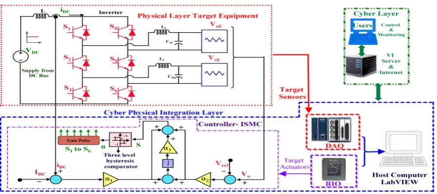
2. Reconfigurable I/O Test Bench - A Cyber Perspective Model 84
The Reconfigurable Input/Output (RIO) based design of Cyber-Physical System RCP evaluation 85
test bench is created for the evaluation of two switch dual output inverter with ISMC control. The 86
experimental setup consists of three sections Physical layer, cyber-physical integration layer, and cyber 87
layer. Fig.6a. shows the configuration of the proposed RCP evaluation of the inverter. The CPS 88
architecture consists of three layers: Physical layer, Cyber Physical integration layer, and Cyber layer. 89
Physical layer comprises of the physical device (target) which needs to be controlled and monitored by 90
CPS. The cyber physical integration layer has the sensors, controllers and software technologies with 91
a host computer to collect the data from the physical device and to control the device based on the 92
responses. The data observed from this layer is monitored and the physical device is controlled by the 93
control center through the internet. The data transfer between the physical device and control center is 94
executed by cyber layer.
Figure 1.Schematic of Mircogrid
95
2.1. Physical Layer: Dual Output Current Source Inverter 96
The microgrid schematic with proposed dual output inverter is shown in Fig.1. The proposed 97
inverter is compared with the family of dual output inverters and given in Table.1. The configuration 98
of proposed dual output current source inverter is shown in Fig.6a. 99
It consists of a DC link reactor with six semiconductor switches. The inverter has two legs with 100
three semiconductor switches and a sharing row of switches for upper and lower output. The inverter 101
is capable of operating at equal voltages (EV) and different voltages (DV).
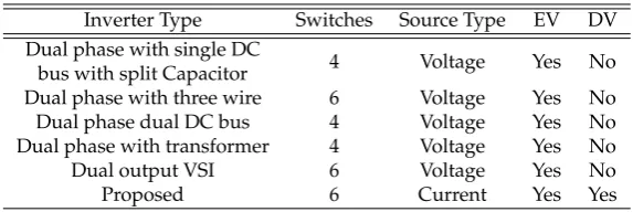
Table 1.Comparison of Inverters
Inverter Type Switches Source Type EV DV
Dual phase with single DC
bus with split Capacitor 4 Voltage Yes No
Dual phase with three wire 6 Voltage Yes No
Dual phase dual DC bus 4 Voltage Yes No
Dual phase with transformer 4 Voltage Yes No
Dual output VSI 6 Voltage Yes No
Proposed 6 Current Yes Yes
Figure 2.System Configuration
2.1.1. Equal voltage (EV) mode of operation 103
In this mode, the two ac outputs voltages are independent and equal. The inverter works similar 104
to a full bridge with two parallel loads. The gate signals for upper (S1,S4) and lower (S3,S6) switches
105
are generated by the control strategy. The control signals for sharing switches (S2,S5) is generated by
106
the logical XOR of the upper and lower signals of the same itself. The instantaneous output voltage 107
(von) of the dual output inverter are same when it operates at EV mode is expressed in (1). 108
von=voU=voL=
∞
∑
n=1,3,5..4VDC
nπ Sinnωt (1)
2.1.2. Different voltage (DV) mode of operation 109
In this operating condition, the inverter is capable of delivering different voltage magnitude. The 110
upper side will act as a full bridge and lower will act as a half bridge. The DV mode is in existence due 111
to the presence of DC link reactor. It will protect the inverter from short circuit and floating modes. If 112
the inverter is operated at different voltage mode, the upper side voltage (voU) will be in full bridge 113
mode as expressed in equation (2) and the lower side (voL) will be in half bridge mode. The output 114
equations for the half bridge are given by (2). 115
voU=
∞
∑
n=1,3,5..4VDC
nπ Sinnωt, voL =
∞
∑
n=1,3,5..2VDC
nπ Sinnωt (2)
2.1.3. System modelling 116
The dual output inverter is modeled based on CSI topology. It comprises the source voltage (VS), 117
a DC link reactor (L), IGBT switches, output capacitive filter (C) and a resistive load (R). The equation 118
of the CSI is written as, 119
LdiDC
dt +riDC=VS−VDC (3)
Cdvo dt =io−
vo
R (4)
where, u is the switching function,VDC =uvois the input DC voltage,io = uiDCis the output AC 120
parameters of dual output inverter, it is assumed thatC=C1f =C2f as dual output capacitive filter 122
andvo =voU =voLas dual output voltage. The state space for the system operation is described in 123
matrix form is given by (5), 124 " ˙ vo ˙ io # = " −r/L −1/L −1/C −1/RC # " vo io # + " 1/L 0 #
u+h0 1i "
vo io #
(5)
The transfer function for the system operation is represented in (6), 125
G(s) =
1 LC S2−S
−L
+RC(−ridc) RCL
+
(−ridcRC−L)LC+RCL RC2L2
(6)
2.2. Cyber-Physical Integration Layer: C-DAQ, RIO with sliding mode controllers 126
Cyber-Physical Integration Layer in a CPS incorporates the algorithm to gather sensor information 127
and issue control signals through actuators to the physical device. This layer has software and 128
hardware coordination in-order to control and monitor the physical device. The CPS should behave as, 129
(A) Intelligent: To predict and understand the behaviour of the system using LabVIEW environment, 130
(B) Real-Time : To gather the real-time data from physical device C-DAQ-9174 is utilised, (C) Adaptive 131
& Predictive control: To respond and anticipate the changes in the physical systems the ISMC based 132
control strategy is implemented in MyRIO-1900 . 133
2.2.1. Sliding Mode Control (SMC) 134
The Sliding Mode Control (SMC) is an effective controller with switching nature of inverter 135
derived from the system model. The advantages of SMC are, it has a better dynamic response, stability 136
against the variations of the load and easy implementation. It consists of inner and outer control 137
loops. The input inductor current and output capacitor voltage is considered as the state variables for 138
controlling. The error variables are given by, 139
Error Variables=
(
x1=iDC−IDC x2=Vo−Vre f
(7)
The sliding surface (S) of SMC is expressed by (8), 140
S=α1x1+α2x2 (8)
Where,α1andα2are the sliding coefficients. The additional variablex3accumulates directly to the
141
steady state errors ofx1andx2. The time derivative of (8) is,
142
˙
S=α1x˙1+α2x˙2 (9)
The derivatives ofx1andx2is given by (10) and (11) ,
143
˙ x1= 1
L(Vs−riDC−uvo)− dIDC
dt (10)
˙ x2=
1 C
uiDC−
vo R
−dVre f
dt (11)
By substituting (10) and (11) in time derivative equation (9) gives (12), 144
˙
S=−uα1 L −
α2
RC
vo+
−α1r L +
α2u
C
Where A is given by (13), 145
A=
α1
Vs L −
dIDCα1
dt −α2 dVre f
dt
(13)
The condition for stabilitySS˙<0 should be satisfied and the control variable is given by, 146
u=−signum(S) (14)
To satisfy the stability condition,u=1 andu=−1 is incorporated to the equation (12).
i f, S<0=S˙>0⇒u=1,
˙
S=h−α1 L −
α2
RC
vo+
−α1r L +
α2
C
iDC+A i
>0 (15)
i f, S>0=S˙<0⇒u=−1,
˙
S=hα1
L −
α2
RC
vo+
−α1r L −
α2
C
iDC+A i
<0 (16)
From equation (15) and (16) the simplified condition for stability is given by (17),
0 <
−α1C+α2L
R
vo + (α2L+α1rC)iDC − LCA < 2(α2LiDC−α1Cvo) (17)
The equivalent continuous control variableueqis given by (18), 147
ueq= LC voCα1−α2L
−α2vo
RC − iDCα1r
L +A
(18)
Theueq maintains the error variables of the systems. The problem withueq is complicated while 148
implementing in analog controllers. For the easy implementation of sliding mode control instead of 149
direct implementation ofueq, the switching relay function is used. The switch relay function is given 150
by (19), 151
ueq= -sign(S) = (
+1 i f S<0
−1 i f S>0 (19)
The switching function is realized bysignumfunction and direct implementation of this function results 152
in uncontrolled switching frequency and no steady-state errors. Operating of CSI in this condition 153
leads to system failure in practical conditions. To operate CSI with limited frequency and controllable, 154
hysteresis band with boundary layer is utilized. The hysteresis band is implemented instead ofsignum 155
function and the function is given by (20), 156
u= (
+1 i f S<−h
−1 i f S>h (20)
The hysteresis bandwidth in S is used to control the dual output CSI with switching frequency, 157
inductor current, and capacitor voltage. If S=0, CSI cannot be controlled. To control dual output CSI, 158
the switching should lie inS =±h. The performance plot for both inductor current and capacitor 159
output voltage is given in Fig.3aand3b. The parameters considered are L = 10mH,C = 20µF, 160
R=50Ω,α1=0.0002,α2=0.2 andα3=50 and are simulated with Matlab.
(a)
(b)
Figure 3.Performance comparision of SMC and ISMC: (a) Input current, (b) Output Voltage
2.2.2. Integral sliding mode control (ISMC) 162
The SMC based control has steady-state errors in both capacitor output voltage and inductor 163
current. It is observed from Fig.3b, the capacitor output voltage is not tracked with the reference 164
voltage and has a steady-state error of 10%. The steady state error of the inductor current is about 165
5% as observed from Fig.3a. As a method to suppress the steady state error of the inductor current 166
and output voltage, an additional integral term of the state variablesx1andx2are introduced to the
167
sliding surface. The additional integral term of error variable is introduced into SMC as an additional 168
control variable and stated as integral sliding mode controller (ISMC). The additional variablex3is
169
considered and it is obtained by integrating the state variablesx1andx2is given by (21),
170
Error Variable=x3=
Z
(x1+x2)dt (21)
The sliding surface (S) of ISMC is expressed by (22), 171
S=α1x1+α2x2+α3x3 (22)
Where,α1,α2andα3are the sliding coefficients. The additional variablex3accumulates directly to the
172
steady state errors ofx1andx2. The time derivative of (22) is,
173
˙
S=α1x˙1+α2x˙2+α3x˙3 (23)
˙
The derivatives ofx1,x2andx3is given by (25), (26) and (27) ,
174
˙ x1= 1
L(Vs−riDC−uvo)− dIDC
dt (25)
˙ x2= 1
C
uiDC−vo R
−dVre f
dt (26)
˙
x3= (iDC−IDC) +
vo−Vre f
(27)
By substituting (25), (26) and (27) in time derivative equation (23) gives (28), 175
˙
S=−uα1 L −
α2
RC+α3
vo+
−α1r L +
α2u
C +α3
iDC+B (28)
Where B is given by (29), 176
B=
α1Vs
L −
dIDCα1
dt −α2 dVre f
dt −α3IDC−α3Vre f
(29)
The condition for stabilitySS˙<0 should be satisfied and the control variable is given by, 177
u=−signum(S) (30)
To satisfy the stability condition,u=1 andu=−1 is incorporated to the equation (29).
i f, S<0=S˙>0⇒u=1,
˙
S=h−α1
L −
α2
RC +α3
vo+
−α1r
L +
α2
C +α3
iDC+B i
>0 (31)
i f, S>0=S˙<0⇒u=−1,
˙
S=hα1
L −
α2
RC +α3
vo+
−α1r
L −
α2
C +α3
iDC+B i
<0 (32)
From equation (31) and (32) the simplified condition for stability is given by (33),
0 <
−α1C+α2L
R−α3LC
vo+ (−α3LC+α2L+α1rC)iDC−LCB < 2(α2LiDC−α1Cvo) (33)
The equivalent continuous control variableueqis given by (34),
ueq = LC
voCα1−α2L
−α2vo
RC +voα3− iDCα1r
L +iDCα3+B
(34)
The information about the sliding mode is given by (33). In the proposed ISMC, the condition for 178
stability in (33) is tested by the numerical computations of the sliding coefficients (α1,α2andα3). The
179
stability is tested along withiDCandvominimum and maximum values. And from (33) the equation 180
(35) can be obtained based on the numerical computations. 181
2(α2LiDC−α1Cvo)>0 (35)
Due to the stability requirement the sliding coefficients (α1,α2andα3) will be in positive. In steady
182
state conditioniDC=IDC. The condition forvois given by, 183
α2
α1
> Cvo
LiDC
The sliding coefficient (α3) will be determined regardless of (α1 andα2) by fine-tuning to obtain
184
the desired response. The block diagram for ISMC is shown in Fig.6a. The switching function is 185
defined by the hysteresis (h) block in the controller design. The hysteresis switching function has three 186
levels (−1, 0,+1). Hysteresis band is fixed based on the reference output voltage (vo). In general, the 187
hysteresis band (h) will be fixed between 5-10%. The instantaneous hysteresis band is calculated based 188
on the frequency (f) and expressed as (37), 189
Hysteresis band = 1
8f L
VDC− 4v2o VDC
(37)
In three-level hysteresis , for+veoperation voltage is+VDCwhen error reaches the lower hysteresis 190
band (hlower,−h) and000when reaches lower then ’-h’. For−veoperation voltage is−VDCwhen error 191
reaches the upper hysteresis band (hupper,+h) and000 when reaches higher than ’+h’. In two-level 192
hysteresis, the no existence of dead band (td) due to the direct transition of+veto−veThe excursion 193
of sliding surface (S) beyond the hysteresis band (h) results in a dead band (td) for semiconductor 194
switches. In three-level hysteresis, the000level existence will result in the dead time for semiconductor 195
switches and has less distortion in output voltage. The switching frequency (fsw) for three-level 196
hysteresis function[11] is calculated based on (38), 197
fsw= ω
2
oVDC h+tdωo2VDC
2
πm−
1 2m
2 (38)
Where, ωo = 2πf, f is the line frequency, m is the amplitude of disturbance. The instantaneous 198
switching frequency (fin) is based on the transition betweenhuppertohlower. The average switching 199
frequency is calculated with the dead-band of 3µsand hysteresis width of 0.05Vµsresulted in the 200
average switching frequency of 2.9kHz and the line frequency is 50Hz. The switching function for the 201
inverter model shown in Fig.6ais given by (39), 202
u1,2 =
(
+1 i f S<−h
0 i f S>0 u4,5= (
−1 i f S>+h 0 i f S<0
u2,3=
(
+1 i f S<−h
0 i f S>0 u5,6= (
−1 i f S>+h
0 i f S<0 (39)
The sliding surface (S) is the input to the schmitt trigger (hysteresis switching). The schmitt trigger 203
is designed to operate as per the switching conditions (39) for generating control signals. The ISMC 204
respond better than SMC and minimized the steady state errors. The ISMC based control strategy is 205
implemented for the dual output single phase inverter. The controller is designed in reconfigurable 206
input/output (RIO) processor. The experimental test bench is created and the performance of the 207
inverter with the ISMC is analyzed. The performance of the SMC and ISMC is analyzed and shown in 208
Fig.3aand3b. The inner current control is analyzed by fixing the reference of 5A and changing the 209
input signal of 6A, 4.5A, 1.5A, and 6A. It is inferred from Fig.3a, the settling time for SMC is 0.01s 210
with steady state error of 10% and ISMC has 0.05s with tracking to reference and alleviates the steady 211
state error in the inductor current. From Fig.3ait is observed that the SMC has the high steady state 212
error compared to ISMC. For the outer voltage control loop analysis, the reference voltage is 120V. It is 213
inferred from Fig.3b, the the steady-state error of SMC is 10% and not tracking the reference voltage and 214
ISMC alleviates the steady state error in the voltage and settles at 0.005s with oscillations. The control 215
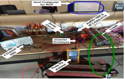
based on SMC has higher steady state error compared to ISMC. The host computer with LabVIEW, 216
C-DAQ, and MyRIO comprises a cyber-physical integration layer as shown in Fig.1. The LabVIEW is 217
a graphical programming tool with seamless integration of hardware for both data acquisition and 218
controlling the physical devices. The source voltage (VABC), source current (iDC), output voltage (Vo), 219
Figure 4.Experimental Setup
and current (NI-9227) sensor. The voltage and current data collected from physical layer are processed 221
in LabVIEW. The acquired signals are monitored in the front panel. the control algorithm for inverter 222
based on ISMC is modeled and block diagram is shown in Fig.1. The controller (actuator) is based 223
on NI-1900 MyRIO (Reconfigurable Input/Output) which has Xilinx Zynq-7010 with a combination 224
of Artix-7 FPGA processor, dual-core ARM Cortex-A9 real-time processor and, onboard WIFI. As 225
an advantage of RIO architecture and WIFI, the physical equipment at a remote location is easily 226
controlled. The terminals are reconfigurable as per the requirements. This leads this test bench to 227
utilize for all power electronics prototype testing. The control algorithm is programmed in NI-My RIO 228
1900 and connected to the physical device gate driver TI SM72295. The experimental setup is shown in 229
Fig.4. 230
2.3. Cyber Layer - LabVIEW based CPS 231
The combination of physical layer and the cyber-physical layer is integrated into the cyber layer. 232
The cyber layer has host computer with server and monitoring station (control center). The data 233
transmission and security is the major concern in the cyber layer. The traditional data transmission is 234
not sufficient to transfer large data in CPS. In order to satisfy the needs, the CPS must have the inbuilt 235
transmission systems. The MyRIO has inbuilt Wi-Fi for data exchange between the host and target. 236
While considering the security of the connection, It utilizes the TCP protocol with SSL.x.509 secured 237
layer to enhance the security. The host computer with LabVIEW has the web service management 238
tool for creating the secured URL. The URL mapping is given byhttps://localhost:port address/web 239
service.html. The LabVIEW has the in-built server for the data exchange with secured network. The 240
collected data from the target is monitored and controlled through the web browser. This method has 241
good live data support, good interaction between the client and user.
Table 2.System Parameters
Parameters Values (Units)
Maximum Rated Power 1kW
DC Voltage(VDC) 120V
Inductor 10mH
IGBT IRG4BC30S
Diodes MUR860
Controller NI myRIO 1900
Data Acquisition Systems NI C-DAQ 9174
Driver Circuit Texas Instruments SM72295
Server NI web server
Network Monitoring Total Network Manager (TNM)
Oscilloscope Textronix TPS 2024B four channel
3. Results and Discussions 243
The performance of the proposed dual output inverter with ISMC control strategy is tested and 244
monitored through the CPS system. The analysis performed under various test conditions like equal 245
output voltage at both upper and lower side, the different output voltage in upper and lower side 246
and inverter analyzed with and without load variations. The control strategy is implemented using 247
reconfigurable input/output (RIO) processor. The hardware prototype is fabricated to demonstrate 248
the proposed inverter. The prototype specifications are given in the Table.2. 249
3.1. Steady state performance 250
The steady state performance of the dual output current source inverter is analyzed with ISMC 251
based control strategy. The tracking performance of ISMC is discussed in Section2.2.2and performance 252
the comparison of SMC with ISMC is plotted in Fig.3band3a. The IMSC alleviates the steady state 253
error and settles at 0.05s. Fig.5shows the performance of dual output inverter with ISMC. The DC 254
voltage (Vdc) and current (Idc) shown in Fig.5a. Due to the current source inverter configuration, the 255
DC link inductor limits the sudden changes in the current and the distortion will get reduced. Fig.5b 256
depicts the dual output voltage and current for 50Hz operation at EV mode. The dual output current 257
source inverter delivers 83V at both load ends (VoU,VoL) due to the DC link of 120V. The upper load 258
current (IoU) 3.60A is observed and lower output current (IoL) is 2.65A. The dual output CSI is, capable 259
of delivering different voltages (DV mode). In this mode, the upper output voltage is similar to full 260
bridge inverter and lower output voltage similar to as half bridge inverter. 261
Fig.5cshows the upper output voltage (VoU) as 83V and lower voltage (VoL) as 38.4V. The upper 262
load current (IoU) observed is 3.80A and lower load current (IoL) observed is 1.68A. The inverter is 263
operated at both EV and DV mode with ISMC. 264
3.2. Response to load variations 265
Fig.5ddepicts the step change in both upper and lower load of the dual output current source 266
inverter when operates at EV mode. The inverter operates at 50Hz, the output voltage of upper (VoU) 267
and lower voltage (VoL) is 83V. The IMSC has a robust response to the load variation and maintains the 268
voltage at the desired level. Fig.5eand5frepresents the dual output current source inverter waveforms 269
when a sudden step change in upper or lower load. Fig.5eshows the upper (VoU) and lower voltage 270
(VoL) respectively. The change in upper load (IoU) and current observed is 1.24A and lower load current 271
(IoL) results in 597mA and waveforms shows the change in load. From Fig.5fthe EV mode operation 272
with step change in upper load is observed with 83V in upper and lower. The load current in 1.24A 273
and 2.51A respectively. In Fig.5g, the performance of the inverter with ISMC. Resultant waveform 274
evidences the operation of the inverter at a different voltage (DV mode) with variations in load current. 275
Fig.5gshows the upper voltage (VoU) 83V and lower voltage (VoL) 38V with variations in upper load 276
current (IoU) and lower load current (IoL). 277
In Fig.5h, the performance of inverter in DV mode with a step change in upper load is analyzed 278
and corresponding upper load current (IoU) is 269mA. The lower load current (IoL) inferred is 1.22A. 279
The overall observations from Fig.5shows that dual output current source inverter has the capability 280
of supplying two independent loads of same (EV mode) and different voltage (DV mode). The 281
dual output current source inverter has the capability of supplying two independent loads of equal 282
(EV mode) and different voltage (DV mode). The dual output inverter can be used in renewable 283
applications to feed simultaneously power to grid and to the stand-alone load. In electric drives 284
applications to operate two different machines of same or different voltage level. The selection of DC 285
link inductor should be concentrated more to obtain the maximum performance of the inverter. Gate 286
pulse generation of the middle switches is critical, due to dual operation. 287
The performance of the inverter is analysed with single phase power quality analyser (Fluke 288
(a)CH1−Vdc,CH2−Idc (b) CH1 − VoU,CH2 −
IoU,CH3−VoL,CH4−IoL
(c) CH1 − VoU,CH2 −
IoU,CH3−VoL,CH4−IoL
(d) CH1 − VoU,CH2 −
IoU,CH3−VoL,CH4−IoL
(e) CH1 − VoU,CH2 −
IoU,CH3−VoL,CH4−IoL
(f) CH1 − VoU,CH2 −
IoU,CH3−VoL,CH4−IoL
(g) CH1 − VoU,CH2 −
IoU,CH3−VoL,CH4−IoL
(h) CH1 − VoU,CH2 −
IoU,CH3−VoL,CH4−IoL
Figure 5.Prototype Results: (a) DC voltage and current, (b) EV mode output voltage and load current, (c) DV mode output voltage and load current, (d) EV mode output voltage and load current with step change, (e) EV mode output voltage and load current with step change in lower load, (f) EV mode output voltage and load current with step changes in upper load, (g) DV mode output voltage and load current with step changes in load, (h) DV mode output voltage and load current with step change in upper load
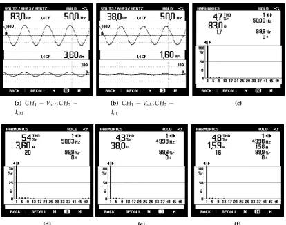
upper voltage (VoU) and upper current (IoU) is observed. Fig.6bshows the lower voltage (VoL) and 290
lower current (IoL). The total harmonic distortion (THD) of upper load voltage and current is observed 291
from Fig.6. Fig.6cdepicts the THD of upper voltage (VoU) is 4.7% and from Fig.6dit is observed that 292
THD of upper current (IoU) is 5.4%. The total harmonic distortion (THD) of lower load voltage and 293
current is observed from Fig.6. From Fig.6ethe THD of lower voltage (VoL) observed is 4.3%. Fig.6f 294
depicts the THD of lower current (IoL) is 4.8%. The THD observed from the results depicts that the 295
(a) CH1−VoU,CH2−
IoU
(b) CH1−VoL,CH2−
IoL
(c)
(d) (e) (f)
Figure 6.Prototype Results: (a) Upper output voltage and load current, (b) Lower output voltage and load current, (c) Upper output voltage THD, (d) Lower output voltage THD, (e) Upper Current THD, (f) Lower Current THD
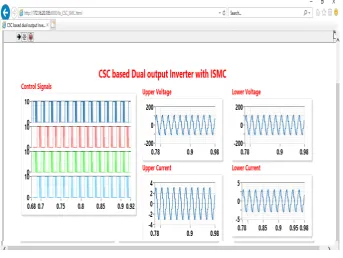
3.3. Online monitoring 297
The CPS design is implemented to evaluate the performance of CSI dual output inverter. The 298
control and monitoring of the target device are done through the internet browser. The connection 299
is based on TCP protocol and SSL.x.509 secured layer is used to ensure the webpage security. From 300
Fig.7the online monitoring of dual output CSC inverter performance is displayed. The resilient cyber 301
infrastructure designed using single domain has the advantage of lower transport delay and easy 302
implementation compared to other methods. The incorporation of CPS in the inverter model leads to 303
the development of smart grids, smart manufacturing in industries for controlling inverters in drives 304
and smart learning with decentralized control of multiple systems. 305
4. Conclusion 306
The dual output current source inverter topology operating in two different voltage mode is 307
presented. A significant advantage of this topology is that it can supply power simultaneously to two 308
different loads of equal (EV mode) and/or different (DV mode) voltages for microgrid applications. 309
The control strategy based on sliding mode controllers is analyzed. The conventional sliding function 310
has the steady state error of 10% for voltage control and 5% for current control. To alleviate the steady 311
state error an additional integral term is introduced and integral sliding mode control is derived for 312
the dual output current source inverter. Reconfigurable Input/ Output processors (MyRIO-1900) 313
Figure 7.Monitoring Screen
processors with high speed data processing is required. The development the cyber physical system 315
for inverter leads to the development of virtual laboratories and smart grids. 316
Conflicts of interest 317
The authors declare that they have no conflicts of interest. 318
Acknowledgements 319
The authors like to thanks the smart grid laboratory, power electronics laboratory and advanced 320
drives laboratory, School of Electrical Engineering, Vellore Institute of Technology(VIT), Chennai for 321
carrying out this project. 322
References 323
1. Pichan, M.; Karimi, M.; Simorgh, H. Improved low-cost sliding mode control of 4-leg inverter for
324
isolated microgrid applications. International Transactions on Electrical Energy Systems2018, p. e2642.
325
doi:10.1002/etep.2642.
326
2. Li, T.; Cheng, Q. Structure analysis and sliding mode control of new dual quasi-Z-source inverter in
327
microgrid. International Transactions on Electrical Energy Systems2018, p. e2662. doi:10.1002/etep.2662.
328
3. Jacobina, C.; de Freitas, I.; Lima, A. DC-Link Three-Phase-to-Three-Phase Four-Leg Converters. IEEE
329
Transactions on Industrial Electronics2007,54, 1953–1961. doi:10.1109/tie.2007.895141.
330
4. Yu, X.; Starke, M.; Tolbert, L.; Ozpineci, B. Fuel cell power conditioning for electric power applications: a
331
summary. IET Electric Power Applications2007,1, 643. doi:10.1049/iet-epa:20060386.
332
5. Fatemi, A.; Azizi, M.; Mohamadian, M.; Varjani, A.Y.; Shahparasti, M. Single-Phase Dual-Output
333
Inverters With Three-Switch Legs. IEEE Transactions on Industrial Electronics 2013, 60, 1769–1779.
334
doi:10.1109/tie.2012.2190952.
335
6. Nguyen, B.L.H.; Cha, H.; Kim, H.G. Single-Phase Six-Switch Dual-Output Inverter Using Dual-Buck
336
Structure. IEEE Transactions on Power Electronics2017, pp. 1–1. doi:10.1109/tpel.2017.2774363.
337
7. Senthilnathan, K.; Annapoorani, I. Implementation of unified power quality conditioner (UPQC) based on
338
current source converters for distribution grid and performance monitoring through LabVIEW Simulation
Interface Toolkit server: a cyber physical model. IET Generation, Transmission & Distribution2016,
340
10, 2622–2630. doi:10.1049/iet-gtd.2015.1040.
341
8. Komurcugil, H. Integral sliding-mode-based current-control strategy for single-phase current-source
342
inverters. Electrical Engineering2011,93, 127–136. doi:10.1007/s00202-011-0197-3.
343
9. Li, R.T.H.; hung Chung, H.S.; Chan, T.K.M. An Active Modulation Technique for
344
Single-Phase Grid-Connected CSI. IEEE Transactions on Power Electronics 2007, 22, 1373–1382.
345
doi:10.1109/tpel.2007.900488.
346
10. Komurcugil, H. Steady-State Analysis and Passivity-Based Control of Single-Phase PWM Current-Source
347
Inverters. IEEE Transactions on Industrial Electronics2010,57, 1026–1030. doi:10.1109/tie.2009.2025297.
348
11. Kukrer, O.; Komurcugil, H.; Doganalp, A. A Three-Level Hysteresis Function Approach to the
349
Sliding-Mode Control of Single-Phase UPS Inverters. IEEE Transactions on Industrial Electronics2009,
350
56, 3477–3486. doi:10.1109/tie.2009.2016512.
351
12. Afghoul, H.; Krim, F.; Babes, B.; Beddar, A.; Kihel, A. Design and real time implementation of sliding
352
mode supervised fractional controller for wind energy conversion system under sever working conditions.
353
Energy Conversion and Management2018,167, 91–101. doi:10.1016/j.enconman.2018.04.097.
354
13. Komurcugil, H.; Biricik, S. Time-Varying and Constant Switching Frequency-Based Sliding-Mode Control
355
Methods for Transformerless DVR Employing Half-Bridge VSI.IEEE Transactions on Industrial Electronics
356
2017,64, 2570–2579. doi:10.1109/tie.2016.2636806.
357
14. Morales, J.; de Vicuna, L.G.; Guzman, R.; Castilla, M.; Miret, J. Modeling and Sliding Mode Control for
358
Three-Phase Active Power Filters Using the Vector Operation Technique.IEEE Transactions on Industrial
359
Electronics2018,65, 6828–6838. doi:10.1109/tie.2018.2795528.
360
15. Ahmadzadeh, S.; Markadeh, G.A.; Blaabjerg, F. Voltage regulation of the Y-source boost DC–DC converter
361
considering effects of leakage inductances based on cascaded sliding-mode control.IET Power Electronics
362
2017,10, 1333–1343. doi:10.1049/iet-pel.2016.0767.
363
16. Musa, A.; Sabug, L.R.; Monti, A. Robust Predictive Sliding Mode Control for Multiterminal HVDC Grids.
364
IEEE Transactions on Power Delivery2018,33, 1545–1555. doi:10.1109/tpwrd.2018.2811560.
365
17. Wang, H.; Ge, X.; Liu, Y.C. Second-Order Sliding-Mode MRAS Observer Based Sensorless Vector Control
366
of Linear Induction Motor Drives for Medium-Low Speed Maglev Applications. IEEE Transactions on
367
Industrial Electronics2018, pp. 1–1. doi:10.1109/tie.2018.2818664.
368
18. Dai, Y.; Zhuang, S.; Ren, H.; Chen, Y.; He, K. Discrete modelling and state-mutation analysis for
369
sliding mode controlled non-isolated grid-connected inverter with H6-type. IET Power Electronics2017,
370
10, 1307–1314. doi:10.1049/iet-pel.2016.0941.
371
19. Yang, Q.; Saeedifard, M.; Perez, M.A. Sliding Mode Control of the Modular Multilevel Converter.IEEE
372
Transactions on Industrial Electronics2018, pp. 1–1. doi:10.1109/tie.2018.2818657.
373
20. Sankar, K.; Jana, A.K. Nonlinear multivariable sliding mode control of a reversible PEM fuel cell integrated
374
system. Energy Conversion and Management2018,171, 541–565. doi:10.1016/j.enconman.2018.05.079.
375
21. Instruments, N. NI Single-Board RIO General-Purpose Inverter Controller Features. Technical report,
376
National Instruments, 2012.
377
22. Balda, J.C.; Mantooth, A.; Blum, R.; Tenti, P. Cybersecurity and Power Electronics: Addressing the
378
Security Vulnerabilities of the Internet of Things. IEEE Power Electronics Magazine 2017, 4, 37–43.
379
doi:10.1109/mpel.2017.2761422.
380
23. van der Meer, A.A.; et.al, P.P. Cyber-physical energy systems modeling, test specification, and co-simulation
381
based testing. 2017 Workshop on Modeling and Simulation of Cyber-Physical Energy Systems (MSCPES).
382
IEEE, 2017. doi:10.1109/mscpes.2017.8064528.
383
24. Yoo, H.; Shon, T. Challenges and research directions for heterogeneous cyber–physical system based on
384
IEC 61850: Vulnerabilities, security requirements, and security architecture. Future Generation Computer
385
Systems2016,61, 128–136. doi:10.1016/j.future.2015.09.026.
386
25. Maffei, A.; et al, S.S. A Cyber-Physical Systems Approach for Implementing the Receding Horizon
387
Optimal Power Flow in Smart Grids. IEEE Transactions on Sustainable Computing 2017, pp. 1–1.
388
doi:10.1109/tsusc.2017.2737144.
389
26. A, L.E. Computing foundations and practice for CPS: A preliminary report. Technical report, University of
390
California, 2007.
27. Liu, Y.; Peng, Y.; Wang, B.; Yao, S.; Liu, Z. Review on cyber-physical systems. IEEE/CAA Journal of
392
Automatica Sinica2017,4, 27–40. doi:10.1109/jas.2017.7510349.
393
28. Andalam, S.; Ng, D.J.X.; Easwaran, A.; Thangamariappan, K. Contract-based Methodology for Developing
394
Resilient Cyber-Infrastructure in the Industry 4.0 Era. IEEE Embedded Systems Letters2018, pp. 1–1.
395
doi:10.1109/les.2018.2801360.
396
29. Nguyen, V.; Besanger, Y.; Tran, Q.; Nguyen, T. On Conceptual Structuration and Coupling Methods
397
of Co-Simulation Frameworks in Cyber-Physical Energy System Validation. Energies2017, 10, 1977.
398
doi:10.3390/en10121977.
399
30. Gonzalez, I.; Calderon, A.; Andujar, J. Novel remote monitoring platform for RES-hydrogen based smart
400
microgrid. Energy Conversion and Management2017,148, 489–505. doi:10.1016/j.enconman.2017.06.031.
401
31. Zhang, F.; Liu, M.; Zhou, Z.; Shen, W. An IoT-Based Online Monitoring System for Continuous Steel
402
Casting. IEEE Internet of Things Journal2016,3, 1355–1363. doi:10.1109/jiot.2016.2600630.
403
32. Moness, M.; Moustafa, A.M. A Survey of Cyber-Physical Advances and Challenges of Wind Energy
404
Conversion Systems: Prospects for Internet of Energy. IEEE Internet of Things Journal2016,3, 134–145.
405
doi:10.1109/jiot.2015.2478381.
406
33. Gonizzi, P.; Ferrari, G.; Gay, V.; Leguay, J. Data dissemination scheme for distributed storage for IoT
407
observation systems at large scale.Information Fusion2015,22, 16–25. doi:10.1016/j.inffus.2013.04.003.
408
34. Zhou, P.; Huang, G.; Zhang, L.; Tsang, K.F. Wireless sensor network based monitoring system for a
409
large-scale indoor space: data process and supply air allocation optimization. Energy and Buildings2015,
410
103, 365–374. doi:10.1016/j.enbuild.2015.06.042.
411
35. Aslan, Y.E.; Korpeoglu, I.; Ulusoy, O. A framework for use of wireless sensor networks in
412
forest fire detection and monitoring. Computers, Environment and Urban Systems 2012, 36, 614–625.
413
doi:10.1016/j.compenvurbsys.2012.03.002.