Polymer Ruled Electronics World
Gopu Krishnan Divya R
Department of Electronic and Telecommunication PG Student
Diploma in Polymer Technology Department of Electronic and Telecommunication GPTC Adoor, Kerala, India MZCE Pathanamthitta, Kerala, India
Abstract
Polymer based electronic devices have vast potential for future electronics development as it has many advantages over conventional inorganic semiconductor based systems, interms of manufacturing, cost, weight, flexibility, and especially the ability to integrate a wide variety of functions on a single platform. Polymer electronics is a unique micro-device technology utilizing plastic diodes, transistors, sensors, light-emitting devices, and photovoltaics among others. Usually the polymer materials can be synthesized chemically, electrochemically and in plasmas. Structural order can be varied from purely amorphous to highly crystalline. Substrate shapes can range from fibers to films. It means that organic materials have more degrees of freedom to work with than inorganic semiconductors. This paper deals with some detailed study about an advanced alternative to convent-ional inorganic fabrication materials.
Keywords: Polymer, ICPs, Polymer devices, Light emitting polymers, OLEDs, OPVs, OFETs
________________________________________________________________________________________________________
I. INTRODUCTION
POLYMERelectronics or organic electronics is a field of materials science concerning the design, synthesis, characterization, and application of organic small molecules or polymers that show desirable electronic properties such as conductivity. In mid 1990’s
all carbon-based (i.e. organic) polymers have been considered to be electrical insulators. But that polymers could be given a degree of conductivity by the addition of quantities of a conductive additive, usually carbon, nickel or silver. It was realized after the discovery of inherently conductive polymers (ICPs), whose conductivity arises from the presence of conjugated carbon-carbon bonds and it is practically used in electronic and optoelectronic applications. ICP was discovered when excess catalyst was added to a batch of polyacetylene the resulting silvery film was doped with various oxidising agents, then the material was found to have become conductive and this resulted in the development of a number of other conductive polymers. The ideal polymer for semiconductor use must meet certain criteria, it must be, a stable suspension, suitable for the deposition method being used, wet the substrate if necessary, and wet the adjoining polymer, cost effective to produce and deposit, have a reasonable shelf life and produce a stable diode.
Fig. 1: Typical semiconductor small molecules.
II. INTRINSICALLY/ INHERENTLY CONDUCTIVE POLYMERS (ICPS)
Electrically conductive polymers can be divided into two groups, depending on the type of charge transport by the carriers responsible for it ionically conductive and elec-tronically conductive. The class of electronically conductive polymers can be further divided into filled and intrinsically conductive polymers (ICPs). Filled systems are rendered electrically conductive by the incorporation of highly conductive metals (usually silver) into the polymer. Intrinsically constructive polymers do not incorporate any conductive additives. ICPs as they are known, gain their electrical conductivity through a property known as ‘conjugation’. Conjugation means that the polymer molecules have alternating double and single bonds and this provides a pathway for free electron charge carriers. Conjugated polymers can be ‘doped’. Doping in polymers is carried out with oxidising or reducing agents that remove or add electrons to the polymer. This oxidation or reduction changes the electronic structure to one that will conduct electricity.
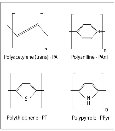
Inherently conductive polymers were accidentally discove-red by a Japanese chemist when excess catalyst was added to a batch of polyacetylene. When the resulting silvery film was doped with various oxidising agents in later work in American laboratories, the material was found to have become conductive and this resulted in the development of a number of other conductive polymers. The most extensively studied conductive polymer systems are these based on the poly-aniline, polythiophene, polypyrrole and polyacetylene.
Fig. 2: Structures of conducting polymers
chemical or electrochemical oxidation or reduction following the polymerisation reaction. The properties, therefore, can be greatly influenced by the degree of oxidation or reduction applied to the original polymer. ICPs exhibit a unique combination of properties, including electrical conductivity, ability to store an electric charge and ability to exchange ions. The values of conductivity of ICP spread across a very wide range and usually increase with an increase in temperature. The preparation of ICPs normally involves a two-stage process. First, the monomer is converted into a polymer with conjugated double bonds; and then the excess charge is introduced using a doping technique. For many applications, ICPs are in competition with commercially available systems of long standing, particularly in the case of polymers loaded with metal particles or carbon fillers. The ICPs therefore need to be superior to conventional filled polymers with respect to the price, ease of recycling at end of life, ease of processing, environmental friendliness and lifetime.
III. POLYMER DEVICES IN ELECTRONICS
The term polymer electronics was shaped for the applicat-ion of these new materials for electronics. Some electronic devices that are fabricated using this are OLEDs, OTFTs, RFID -tags, solarcells, sensors, actuators etc.
Organic Light Emitting Diodes(OLEDs)
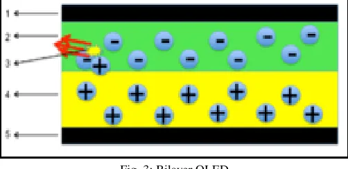
An OLED (organic light-emitting diode) consists of a thin film of organic material that emits light under stimulation by an electric current. A typical OLED consists of an anode, a cathode, OLED organic material and a conductive layer.
Fig. 3: Bilayer OLED.
The OLED device incorporated a double layer structure motif consisting of separate hole transporting and electron-transporting layers, with light emission taking place in between the two layers. The schematic of a bilayer OLED is shown in figure 3 with 1. Cathode (-), 2. Emissive layer, 3. Emission of radiation, 4. Conductive layer and 5.Anode(+).OLED organic materials can be divided into two major families: small-molecule-based and polymer-based. Small molecule OLEDs (SM_OLEDs) include organometallic chelators (Alq3), fluorescent and phosphorescent dyes, and conjugated dendrimers. Fluorescent dyescan be selected according to the desired range of emission wavelengths; compounds like perylene and rubrene are often used. Recently reported a pure organic light emitting crystal, Br6A, by modifying its halogen bonding, they succeeded in tuning the phosphorescence to different wavelengths including green, blue and red. By modifying the structure of Br6A, scientists are attempting to achieve a next generation organic light emitting diode. Devices based on small molecules are usually fabricated by thermal evaporation under vacuum. While this method enables the formation of well controlled homogeneous film; is hampered by high cost and limited scalability. An OLED should require high efficiency and long lifetime, as well as low-cost fabrication, a wide-gamut for sets of devices and high color saturation. OLEDs have demonstrated all of these properties; however, large area fabrication remains a significant challenge, making manufacturing costs quite high. Another technological challenge is the device lifetimes for deep blue devices. There are a large number of stable red and green phosphorescent emitters, giving device lifetimes approaching 106 hours.
Light Emitting Polymers (LEPs)
(4) chemical and thermal stability; and (5) processability which involves solubility, solution viscosity, and solvent-substrate compatibility. These properties can be adjusted by changing the chemical structure of the conjugated polymer chains, side groups, incorporation of heteroatoms, molecular weight, structural regularity and copolymerization.
Organic Photovoltaic Devices (OPVs)
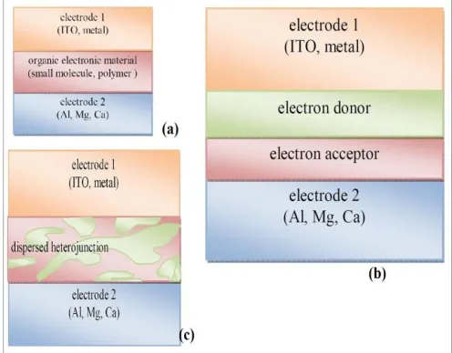
An organic solar cell or plastic solar cell is a type of photovoltaic that uses organic electronics, a branch of electronics that deals with conductive organic polymers or small organic molecules, for light absorption and charge transport to produce electricity from sunlight by the photovol-taic effect. An example of an organic photovoltaic is the polymer solar cell. The molecules used in organic solar cells are solution-processable at high throughput and are cheap, resulting in low production costs to fabricate a large volume. Combined with the flexibility of organic molecules, organic solar cells are potentially cost-effective for photovoltaic applications. Molecular engineering can change the band gap, allowing for electronic tunability. The optical absorption coefficient of organic molecules is high, so a large amount of light can be absorbed with a small amount of materials, usually on the order of hundreds of nanometers. Single layer organic photovoltaic cells are the simplest form. These cells are made by sandwiching a layer of organic electronic materials between two metallic conductors, typically a layer of indium tin oxide (ITO) with high work function and a layer of low work function metal such as Aluminum, Magnesium or Calcium. The basic structure of such a cell is illustrated in Figure 4(a). Bilayer cells contain two layers in between the conductive electrodes (Fig.4(b)). The two layers have different electron affinity and ionization energies, therefore electrostatic forces are generated at the interface between the two layers. The materials are chosen to make the differences large enough that these local electric fields are strong, which splits excitons much more efficiently than single layer photovoltaic cells. The layer with higher electron affinity and ionization potential is the electron acceptor, and the other layer is the electron donor. This structure is also called a planar donor-acceptor heterojunction. Bulk heterojunctions have an absorption layer consisting of a nanoscale blend of donor and acceptor materials. The domain sizes of this blend are on the order of nanometers, allowing for excitons with short lifetimes to reach an interface and dissociate due to the large donor-acceptor interfacial area. However, efficient bulk heterojunctions need to maintain large enough domain sizes to form a percolating network that allows the donor materials to reach the hole transporting electrode (Fig. 4(c)) and the acceptor materials to reach the electron transporting electrode. Without this percolating network, charges might be trapped in a donor or acceptor rich domain and undergo recombination.
Fig. 4: Sketch of OPV cell. (a) single layer, (b) bilayer and (c) bulk heterojunctions OPV.
A new isotropic organic semiconductor for OPVs and OLEDs is Tris[4-(5-dicyanomethylidenemethyl-2-thienyl) phenyl]amine (TDCV-TPA). TDCV-TPA is soluble in a large
variety of organic solvents and can be used for the fabrication of heterojunction solar cells with high open circuit voltage (1.15 V), efficiency close to 2% and longer ambient condition lifetimes than cells based on poly(alkylthiophenes). The compound absorbs at 509 nm and 538 nm as thin film. It can be used as high spectral purity luminophore in LEDs, emitting red light at 658 nm. Its structure is as shown in figure 5.
Organic Field Effect Transistor (OFET)
An Organic field-effect transistor is a field-effect transistor utilizing organic molecules or polymers as the active semiconducting layer. A field-effect transistor(FET) is any semiconductor material that utilizes electric field to control the shape of a channel of one type of charge carrier, thereby changing its conductivity. Two major classes of FET are n-type and p-type semiconductor, classified according to the charge type carried. In the case of organic FETs (OFETs), p-type OFET compounds are generally more stable than n-type due to the susceptibility of the latter to oxidative damage. Like OLEDs, OFETs can be classified into small-molecule and polymer-based system. Charge transport in OFETs can be quantified using a measure called carrier mobility; currently, rubrene-based OFETs show the highest carrier mobility of 20–40 cm2/(V·s). Another popular OFET material is Pentacene. Due to its low solubility in most organic solvents, it's difficult to fabricate thin film transistors (TFTs) from pentacene itself using conventional spin-cast or, dip coating methods, but this obstacle can be overcome by using the derivative TIPS-pentacene. Current research focuses more on thin-film transistor (TFT) model, which eliminates the usage of conductive materials. One common feature of OFET materials is the inclusion of an aromatic or otherwise conjugated π-electron system, facilitating the delocalization of orbital wave functions. Electron withdrawing groups or donating groups can be attached that facilitate hole or electron transport. OFETs employing many aromatic and conjugated materials as the active semiconducting layer have been reported, including small molecules such as rubrene, tetracene,pentacene, diindenoperylene, perylenediimides, tetracyanoquinodimethane (TCNQ), and polymers such as polythiophenes (especially poly(3hexylthiophene) (P3HT)), polyfluorene, polydiacetylene, poly(2,5-thienylene vinylene), poly(p-phenylene vinylene) (PPV). Three essential components of field-effect transistors are the source, the drain and the gate. Field-effect transistors usually operate as a capacitor. They are composed of two plates. By the properties of the carrier, three types of FETs classified as shown schematically in Figure 6. They are MOSFET (metal–oxide–semiconductor field-effect transistor), MESFET (metal–semiconductor field-effect transistor) and TFT (thin-film transistor).
MISFET
The most prominent and widely used FET in modern microelectronics is the MOSFET. There are different kinds in this category, such as MISFET (metal–insulator–semiconductor field-effect transistor), and IGFET (insulated-gate FET). A schematic of a MISFET is shown in Figure 6(a). The source and the drain are connected by a semiconductor and the gate is separated from the channel by a layer of insulator. If there is no bias (potential difference) applied on the gate, the band bending is induced due to the energy difference of metal conducting band and the semi-conductor Fermi level. Therefore, a higher concentration of holes is formed on the interface of the semiconductor and the insulator. When an enough positive bias is applied on the gate contact, the bended band becomes flat. If a larger positive bias is applied, the band bending in the opposite direction occurs and the region close to the insulator-semiconductor interface becomes depleted of holes. Then the depleted region is formed. At an even larger positive bias, the band bending becomes so large that the Fermi level at the interface of the semiconductor and the insulator becomes closer to the bottom of the conduction band than to the top of the valence band, therefore, it forms an inversion layer of electrons, providing the conducting channel. Finally, it turns the device on.
MESFET
The second type of device MESFET (metal semicondu-ctor FET) is described in Fig.6(b). The only difference of this one from the MISFET is that the n-type source and drain are connected by an n-type region. In this case, the depletion region extends all over the n-type channel at zero gate voltage in a normally “off” device (it is similar to the larger positive bias in MISFET case). In the normally “on” device, a portion of the channel is not depleted, and thus leads to passage of a current at zero gate voltage.
TFT
Fig. 6: Schematic of FETs (a)MISFET, (b) MESFET and (c) TFT.
Fig. 7: Rubrene-OFET with highest charge mobility.
OFETs adopt the architecture of TFT. With the development of the conducting polymer, the semiconducting properties of small conjugated molecules have been recognized. The interest in OFETs has grown enormously in the past ten years. The reasons for this surge of interest are manifold. The performance of OFETs, which can compete with that of amorphous silicon (a-Si) TFTs with field-effect mobilities of 0.5–1 cm2 V−1 s−1 and ON/OFF current ratios (which indicate the ability of the device to shut down)
of 106–108, has improved significantly.
IV. CONCLUSION
Polymer electronic devices are not primarily a replacement for existing electronic technologies, but opens up the prospect of completely new applications with the freedom of design, flexibility and low cost of plastics. Polymer devices have many advantages than other as it has low cost, small size and light in weight. By using polymer devices, we can compensate the lack of availability of semiconductors especially silicon. Electronic wastes are a major problem so polymer is a best replacement to avoid e-wastes. Polymer technology is going to give tough competition to conventional semiconductor devices.
REFERENCES
[1] Ridam Misra,“ Role of Poolymers in Materials Science”, cjlscience, June 2015.
[2] David R, Wheeler, Shawn M Dirk, et.al, “Polymer Electronic Devices”, Sandia laboratories publications, Nov 2006. [3] John Gould, “Polymer Electronics”,dti 2004.