DESIGN OF HIGH PERFORMANCE DOUBLE DATA
RANDOM ACESS MEMORY CONTROLLER FOR
MULTIPLE APPLICATIONS
Yelchuri Venkata Suresh Babu
1, Siva Shnaker
2, L.Srinivas Reddy
3 1M. Tech Scholar (DECS), Nalanda Institute of Engg and Tech. (NIET),
Siddharth Nagar, Guntur, A.P, (India)
2
Asst. professor (
ECE
), Nalanda Institute of Engg and Tech. (NIET),
Siddharth Nagar, Guntur, A.P, (India)
3
Assistant. Professor (ECE), Nalanda Institute of Engg and Tech. (NIET),
Siddharth Nagar, Guntur, A.P. (India)
ABSTRACT
In this paper we are presenting a memory controller which is used to control the DDR SDRAM. The memory
uses the 2n pre fetch architecture. The external bus width is half of the width of internal bus width. Its memory
single read /write cycle of 2n bits wide needs one clock cycle at memory core and at the input/output core it
needs one half cycle of clock. The bidirectional signals are provided are called strobe signals. These are the
signals used to align the data at the receiver. The controller make use of delay lines to track DQ signals with the
DSQ to track them. For controlling DDRSDRAM, we proposed memory controller in this paper. The signals
which are used to the capture the signal at the receiver is called strobe signals. These will be used as a part of
data. That formation depend upon the operation it is performing. Nowadays designers using conventional IP
cores connecting to the memories to achieve controlling. Here we have designed a memory controller which can
be used in any type of applications. This controller is designed in Verilog HDL. That design is synthesised in
Xilinx ISE 13.2 I.
Key Words: DDR SDRAM, DSQ, DQ, Read, Write Cycle
I. INTRODUCTION
Nowadays electronic computing devices are getting faster such as microprocessor, CPU. The memory systems
has to become fast. So that complete system performance would be improved. To enhance the speed of data
transfer we developed a new technology of ram called DDR. The name DDR is referred to as double data rate
dynamic memory. This memory is provided with the system clock as like as regular memories. The DDR is
faster than SDRAM since DDR will transfer the data on both edges i.e. on rising edge and falling edge of the
clock. The data rate of DDR is having twice the speed of Single SDRAM. Basically memories are of two types
as follows RAM and ROM.
1.1 Random Access Memory
This is the best example for the computer program memory. This is temporary memoru ehich is used to store
address connected to the specific cell. While during the operation the operands are brought into the RAM. The
RAM is of two types
1) SRAM
2) DRAM
1.2 Static RAM
Static ram is basically built by the inverters. It holds the data in cross coupled inverters. Faster caches are
designed using SRAM. This is having higher cost and less density. Its memory capacity is limited.
1.3 Dynamic RAM
It is slower than the static ram. This is naturally used as program memory due to its denser and refreshing
nature. This is built by the capacitor with a switch to access it. Usually capacitor having periodic charging and
discharging.
DRAM will work based on charge present at the capacitor. By sending exact charge through the column access
make the transistor on attached to it. For write operation capacitor makes on. For reading operation sense
amplifiers connected to it will read the data on it. If the charge on it is 50 percent or more it will read as 1 else
read as 0.
DRAM chip require two CPU wait states to execute the any operation. It can execute any one operation at time
either read or write. The capacitor in the DRAM will discharge after specific interval of time to zero.
1.4 DDR SDRAM
It is referred as Double Data rate SDRAM, which manipulates working of the computer systems due to its
performance difference between them. This device is facilitated with the large bandwidth. This is needed in
operations of huge stream of bits. This memories majorly used in the embedded memories where they are
facilitated with the high speed, portability, pipelining and burst access due to its large bandwidth.
II. SYNCHRONOUS DRAM
The SDRAM may be synchronous or asynchronous. If the DRAM is asynchronous. It has to respond rapidly
with the changes in the control inputs. It will responds to the changes in the input only when clock is
synchronised with inputs. This clock ensures that high speed operation. DDR SDRAM allows data in the form
of bursts of 16bit or 32bit. The bursts may be byte, half word and a word. This supports the strobe signal which
is generated externally and transmitted with data for capturing correct data at the receiver. The strobe signal
DQS is transmitted along with the data. It is edge aligned with the data for read operation. During write cycle
the signals are aligned centrally which was accomplished by the controller. To make read or write into/from the
memory we should initiate memory access by the initiation of Active command. After that read, write is
performed. The access usually happen in way that address bits with the Active commands are used to select
memory bank and corresponding row access. The address bits coherent with read or write operation used to
select column access in the particular memory bank.
This DDR SDRAM is facilitated with the auto pre charge function which means row of location can be self pre
charged after completion of any operation on it. We will enhance the speed by providing additional feauters are
III.PROPOSED SDRAM CONTROLLER
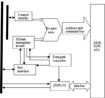
Fig 2.1 DDR Ram Controller
The high speed dynamic ram gives flexibility and reduce the hardware resources required to construct it. That
may be accomplished by providing bypass mode to it which makes CPU to control the interface. The initiation
code given to the CPUs.
3.1 Control Interface
Core mode and set timings are operated by the control interface. This interface also used to work on registers
which are provided by the CSR bus with low speed. The DDR SDRAM address and control buses are used by
the control interface when it is in the bypass mode. In this mode the memory controller is disabled. The Central
processing unit manages the all ports of memory with bypass register. The bypass mode generally used during
boot up sequence. The CPU will monitors the initialization process.
3.2 Management Unit
The address and data buses of the DDR SRAM is operated by the management unit.it lose the control when
bypass mode is activated. The cpu will coordinate the function of SDRAM. This unit provides read and write
control commands, pre charging the banks. The refreshing period of the dynamic ram can also be controlled by
3.3 Data Path Controller
Data path controller controls the way in which data is transferred and amount data to be transferred. Those
operations are managed by the strobe signals DQ and DSQ signals. This adds delay to the read and write
commands from the management unit.
3.4 Bus Interface Unit
This unit is used to send the commands from the SDRAM to the Fast memory link. BIU will acknowledge it
after completion of each cycle.
The fast memory link features are
1) Synchronism. The bus is used for the devices which having architectures use of synchronism
2) Burst data. For every data transfer initiated by the address cycle and then followed by several data bits are
transformed in several clock cycles.
3) Pipelined transfer. After completion each data cycle the new address cycle is initiated by the control lines.
3.5 FIFO
Data Burst and read FIFO techniques are applied to the speed up data transactions between FML and FIFO. To
make any data access to FML bus from the SDRAM has to check that if the data is available in the read FIFO or
if the address of that is within the range of read FIFO or its corresponding valid vector is true. When the valid
vector is true that denotes its respective information is correct. The memory cache having the bit tag for
searching any word in main memory the valid vector is same like as tag.
The size of read FIFO is same as size of burst in SDRAM. So valid-vector length is small since data size of is
FIFO is small. The Fast memory link will get the data if it will present in the memory. The controller will give
the read command to the SDRAM controller. After predefined number of clock cycles data is made available at
the latches of SDRAM. That data will be read by the SDRAM and transferred to the Fast memory link. The data
latches are used to bring the data in to the FML the valid-vector is identification of the of present in the read
FIFO
3.6 Features of DDR SDRAM
1. It supports 2,4,8 bit bursts of data transfer
2. Its having bypass mode for initialization sequence memory
3. It supports burst data for read and write cycle
IV. FINITE STATE MACHINE MODEL OF DDR SDRAM
DDRSRAM functioning is essayed by using the state machine. When the power is on, it will be in same state.
Based upon the control signals issued by the controller the memory will move to the next state. A Pre charge
command is used to deactivate any row in the bank. If this operation is performed the row is empty state. ACT
signal is used to activate any row in the memory bank. After activating the any row, we give read / write
command which is used for data transfer to/from memory. If read command is given memory read operation is
operation controller again gives pre charge all command. Auto refresh command is used to for refresh the
memory since it is dynamic RAM.
DDRSDRAM controller is responsible for all the commands given by it. DDR SDRAM responds to the
commands and it will respond to the commands and acknowledge them. It performs operation based on the
given command from the state machine.
V. SIMULATION RESULTS
In this paper we re designing the Dynamic Ram controller which yields high speed because of double data
rate,larger bandwidth and burst of data. This memory controller is designed using Verilog HDL and synthesised
in Xilinx ISE 13.2 I. The synthesised wave forms proved that it is performing data transfer at faster rate.
VI. CONCLUSION
The DDR SDRAM is the double data rate Synchronous dynamic RAM. It is very fast. The system clock is
synchronised with inputs. It will work with double speed than SDRAM. It’s having higher bandwidth. It
This controller is facilitated with the Bypass mode. In this mode controller is disabled, the SDRAM pins are
controlled by the CPU. The CPU will handle the operation. By the help of bypass register. This includes that
initialization code is managed by the CPU. This controller yields higher speed and higher throughput with
compared to the previous design of RAM controller and SDRAM controller.
VII. REFERENCES
[1]. Design and Implementation of High Performance Dynamic Memory Controller by Sushil Kumar Pachauri
and Suvendra Sahoo. Advance in Electronic and Electric Engineering. ISSN 2231-1297, Volume 4.Number
6 (2014), pp. 617-622
[2]. An IEEE journal on Design and Implementation of DDR SDRAM Controller Based on FPGA in Satellite
Navigation System Li Wang, Ju Wang, Qian Zhang Department of Information and Electronics, Beijing
Institute of Technology,ICSP2012 Proceedings.
[3]. Design and VLSI Implementation of DDR SDRAM Controller for High Speed Applications Deepali
sharma,Shruti bhargava , Mahendra VuchaInternational Journal of Computer Science and Information
Technologies, Vol. 2 (4) , 2011, 1625-1632
[4]. Bandwidth, Area Efficient and Target Device Independent DDR SDRAM Controller by T. Mladenov, F.
Mujahid, E. Jung, and D. Har , Proceedings Of World Academy Of Science, Engineering And Technology
Volume 18 Dec 2006 Issn 1307-6884
[5] Application of DDR Controller for High-speed Data Acquisition Board by Zude Zhou, Songlin Cheng, and
Quan Liu School of Information Engineering, Wuhan University of Technology, Proceedings of the First
International Conference onInnovative Computing, Information Control (ICICIC'06) IEEE
AUTHOR DETAILS
YELCHURI VENKATA SURESH BABU, pursuing his M.tech (DECS) from
Nalanda institute of Engineering and Technology(NIET), Siddharth Nagar,
Kantepudi village, Satenepalli mandal, Guntur Dist., A.P, INDIA. His interest in
digital concepts and specialized in designing of memory blocks.
S. SIVA SANKER REDDY, has completed his M.tech degree and currently he
has been working as an Asst. professor (SSP) in Nalanda institute of Engineering
and Technology (NIET), Siddharth Nagar, Kantepudi village, Satenepalli
mandal, Guntur Dist., A.P, INDIA. He is specialized in signal processing
concepts and data transformation in a system.
L.SRINIVAS REDDY, He completed his post-graduation in DECS. His area of
interest includes digital electronics, digital communication, digital system design
and VLSI technology and design. His research areas are optimal communication
technology. He is currently working as Asst.professor (ECE) from Nalanda
institute of Engineering and Technology (NIET), Siddhartha Nagar, Kantepudi