FPGA IMPLENTATION OF REVERSIBLE
FLOATING POINT
MULTIPLIER USING CSA
Vidya Devi M
1, Lakshmisagar H S
11 Assistant Professor, Department of Electronics and Communication
BMS Institute of Technology,Bangalore
Pankaj Kumar Singh
2, Nitesh Kumar
2, Pitamber kumar
22 Students, Department of Electronics and Communication
BMS Institute of Technology, Bangalore
Abstract- Reversible logic is a promising field of research that finds applications in low power computing, quantum computing, optical computing, and other emerging technologies. Further, floating point multiplication is one of the most widely used operations in image and digital signal processing applications. The single precision reversible floating-point multiplier using Carry save adder requires the design of efficient 24×24 bit integer multiplier. In this work, we have designed a new reversible design of single precision floating point multiplier based on operand decomposition approach and Wallace Tree Multipliers. To design the reversible 24×24 bit multiplier the operands are decomposed into three partitions of 8 bits each. Thus, the 24×24 bit reversible multiplication is performed through nine reversible 8×8 bit Wallace tree multipliers, whose outputs are then summed. A new reversible design of the 8×8 bit Wallace tree multiplier has been implemented. Finally, for the summation stage we have carefully chosen and arranged the reversible half adders and full adders in such a way to yield an efficient multiplier optimized in terms of quantum cost, delay, and garbage outputs.
Key words: FPGA, Reversible logic gates, reversible logic circuits, reversible multiplier circuits.
I. INTRODUCTION
have the lowest quantum cost compared to other reversible logic gates. The optimized values of quantum cost, gate delay, and garbage output is obtained compared to the existing design and reduces the hardware complexity of the system. Section 2 gives the different types of the reversible logic gates required for the present work. Section 3 describes the design of reversible multiplier circuit. Section 4 discusses the design of reversible exponent addition. Section 5 deals with the final results and conclusion.
II. REVERSIBLE LOGIC GATES
A reversible logic gate is an n-input n-output logic device with one-to-one mapping (the number of inputs are equal to the number of outputs). The outputs can be determined from the inputs and also the inputs can be recovered from the outputs. Reversible circuits should be designed using minimum number of reversible logic gates. The parameters to determine the complexity and performance of circuits in reversible logic are as follows:
The number of Reversible gates (N): The number of reversible gates used in circuit.
The number of constant inputs (CI): The number of inputs that are to be maintained constant at either 0 or 1 in order to synthesize the given logical function.
The number of garbage outputs (GO): This refers to the number of unused outputs present in a reversible logic circuit. The garbage outputs cannot be avoided as these are very essential to achieve reversibility.
Fig 1 and 2 shows the classical gate (irreversible gate) and general NxN reversible gate.
Fig 1: Classical (Irreversible) gate
Fig 2: N x N Reversible gate
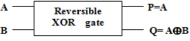
In the reversible XOR gate there is no loss of information bit signals. Since it maps the input vector with output vector which gives the equal number of inputs and output and it is shown in Fig 3.
Fig 3: Reversible XOR gate
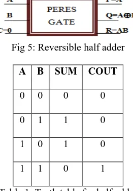
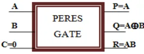
Peres gate is represent as 3×3 vector in Fig 4. In the proposed design, Peres gate is used because of its lowest quantum cost. Quantum cost of a Peres gate is 4.
ADDER AND SUBTRACTOR USINGN PERES AND TR GATES A. Half Adder:
Peres gate is used to realize the different logical functions. For the design of single precision floating point multiplier, reversible half adder (RHA) is obtained from Peres gate with the hardwired control of c=0. The expression became as Q=A⨁B, R =AB which is equal to the sum and carry out of half adder.
Fig 5: Reversible half adder
A B SUM COUT
0 0 0 0
0 1 1 0
1 0 1 0
1 1 0 1
Table 1: Truth table for half adder
B. Full Adder:
Reversible full adder (RFA) circuit is obtained by cascading the two Peres gate as shown in Fig 6. The sum and carry output of reversible full adder is given by the Boolean expression as shown.
Fig 6: Reversible full adder
A B C SUM COUT
0 0 0 0 0
0 0 1 1 0
0 1 0 1 0
0 1 1 0 1
1 0 0 1 0
1 0 1 0 1
1 1 0 0 1
1 1 1 1 1
C. Half Subtractor:
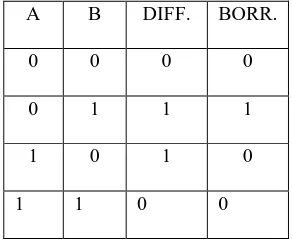
Reversible half subtractor (RHS) is obtained from TR gate with the hardwired control of c=0. The expression became as Q=A⨁B, R =A’.B which is equal to the difference and borrow out of half subtractor.
Fig 7: Reversible half subtractor
A B DIFF. BORR.
0 0 0 0
0 1 1 1
1 0 1 0
1 1 0 0
Table 3: Truth table for half subtractor
D. Full Subtractor:
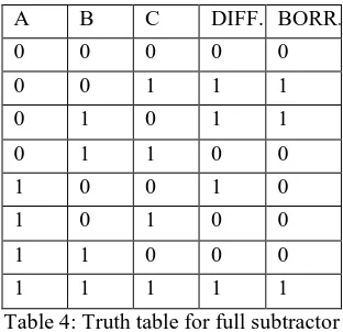
Reversible full subtractor (RFS) circuit is obtained by cascading the two TR gate as shown in Fig 8.The difference and borrow output of reversible full subtractor is given by the Boolean expression as shown.
A B C DIFF. BORR.
0 0 0 0 0
0 0 1 1 1
0 1 0 1 1
0 1 1 0 0
1 0 0 1 0
1 0 1 0 0
1 1 0 0 0
1 1 1 1 1
Table 4: Truth table for full subtractor
III. DESIGN OF REVERSIBLE SPFP MULTIPLIER
Block diagram shown in fig 9 below represent the design of reversible single precision floating point multiplier (RSPFPM).
Fig 9: Block diagram of Reversible Single Precision Floating Point Multiplier[1].
The sign magnitude of the product is obtained by XORing the sign bit (MSB bit) of both the input that is X and Y. Exponent addition is done using reversible ripple carry adder. Since here the input is converted in to IEEE754 format so the bias value (-127) is subtracted using ripple borrow subtractor. For the design of 24 x 24 bit multiplier, first there is addition of 1 bit to both the input so that it will become 24 bit and then it is divided in to three parts 8 bit each. The design is developed using Verilog code and simulation of result is obtained in Xilinx software tool.
A. Single Precision Floating Point Number
IEEE754 standard format consist of three part first part is sign bit which is of single bit(S), second part is exponent bit(E) which is of 8 bit and last part is mantissa bit(M) which is of 23 bit as shown in fig 10.
B. Xoring of sign bit
Sign bit can be xor using peres gate with third input zero.
Fig 11: Sign XORing
C. Exponent addition
Exponent addition is done using 8 bit ripple carry adder. Why we are going for ripple carry adder is because 24 x 24 bit multiplication is going to take more time as compare to this addition. The block diagram is shown below.As mention in the block diagram 127 is subtracted from the result obtain after the addition so for that ripple borrow subtactor is used. This subtractor is design using TR gate.
D. Multiplication of mantissa part
First there is addition of 1 bit to each of the 23 bit mantissa part to make it in to 24 bit (standard format) after that it is divide it in to 3 parts 8 bit each then an 8 multiplier is designed using reversible gate and result is obtained. Multiplication has two parts
1) Generation of partial products
2) Addition of partial products: For the generation of partial products peres gate is used as an AND gate.
Fig 12: ANDing operation
The third output of peres gate is the AND operation of the two input
CARRY SAVE ADDER:
A carry-save adder is a type of adder, used in computations to calculate the sum of n-bit binary numbers such that it outputs two numbers of the same dimensions as the inputs, one which is the sum and the carry.If the number of inputs to the adder are ‘n’ 1 bit numbers, then the output is log2n bits. Figure 13 shows the block diagram of carry
Fig 13: Carry save adder
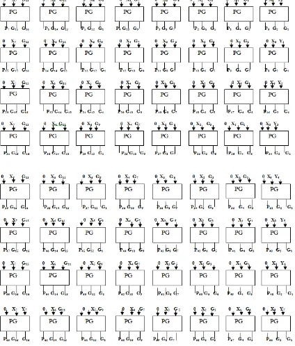
The 64 partial products are obtained for 8x8 bit reversible multiplication X × Y= ([x7, x6, …. x0 ] x [y7, y6,…. y0 ]) and is shown in Fig 14
After the generation of partial products the next part is addition of the partial products for the carry save adder is used.The carry-save adder reduces the addition of 3 numbers to the addition of 2 numbers. The propagation delay is 3 gates regardless of the number of bits. The carry-save unit consists of n full adders, where each of the adders calculates a single sum and carry bit based on the corresponding bits of the three input numbers. The entire sum can then be computed by shifting the carry sequence left by one place and appending a 0 to the front (most significant bit) of the partial sum sequence and adding this sequence with RCA produces the resulting n + 1-bit value. This process can be continued continously, adding an input for each stage of full adders, without any carry propagation to the next stage. These stages can be arranged in a binary tree structure, with cumulative delay logarithmic in the number of inputs to be added, and invariant of the number of bits per input. The main application of carry save algorithm is, well known for multiplier architecture is used for efficient CMOS implementation of much wider variety of algorithms for high speed digital signal processing.CSA applied in the partial product line of array multipliers will speed up the carry propagation in the array. Addition of partial products of 8x8 multiplier using carry save adder is shown in Fig 15
Fig 15: Addition of partial products of 8x8 multiplier
Since carry save adder is using half adder and full adder so this fig shows how it is going to use the red circle is half adder and blue circle is full adder and the dots are sum and carry. At last it is stage of addition it is using ripple carry adder.
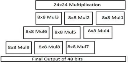
Using this 8x8 multiplier 9 times the 24x24 multiplier is obtained as shown in the Fig 16.
Fig 16: block diagram of 24x24 using 8x8 multiplier
E. Final result
IV. RESULT ANALYSIS & SIMULATION OUTPUT
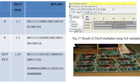
With the help of code written in Verilog the test bench verification of the 32x32 multiplier is done based on the logic explain above.
Fig 17: Result of 24x24 multiplier using 8x8 multiplier
The table shown below is the comparison of delay of 4 bit ripple carry adder and 4 bit carry save adder with the constrains provided by the system. If user constrains are provided in cadence then the delay difference will be more.
ADDER DELAY
Ripple carry adder 15.422ns Carry save adder 13.66ns
Table 5: Comparison between ripple and carry save adder
V. CONCLUSION
32 bit reversible single precision floating point multiplier uses the reversible half adder, full adder, reversible 8X8 multiplier to implement an efficient multiplier having faster execution time and gate delay. Comparison of delay between carry save adder (CSA) and ripple carry adder (RCA) is done. Since delay in CSA is less so it is used for addition of partial products. This proposed multiplier can be used to design complex system in nanotechnology and also used to design a reversible exponent calculator with high precision values.
REFERENCES
[1] M.Jenath, V Nagrajan, ”FPGA implementation on Reversible floating Point Multiplier “IJSCE, March 2012.
[2] Mohamed Al-Ashrafy, Ashraf Salem and Wagdy Anis, “An efficient implementation of Floating Point Multiplier,978-1-4577-0069-9, IEEE-2011.
DECI
MAL
BINARY
X 1.1 00111111100011001100110
011001101
Y 1.3 00111111101001100110011
001100110
OUT
PUT
1.43 00111111101101110000101
000111101
01000010100011110101110
[3] D. Maslov and D. M. Miller. Comparison of the cost metrics for reversible and quantum logic synthesis,http://arxiv.org/abs/quant- ph/0511008, 2006.
[4] John G. Proakis and Dimitris G. Manolakis (1996), “Digital Signal Processing: Principles,. Algorithms and Applications”, Third Edition.
[5] Michael Nachtigal, Nagarjan Ranganathan,” Design of single precision floating point multiplier based on operand decomposition”, 10th
IEEE International Conference on nanotechnology joint symposium with Nano Korea, August 2010.