Spectroscopic ellipsometry, optical, structural and electrical
investigation of sprayed pure and Sn-doped ZnO thin films
Mokhtari H. (1,*), Benhaliliba M. (1), Aida M.S.(2), Attaf N.(2)and Y. Ocak (3)
(1) Physics Department, Sciences Faculty, USTO-MB University, BP1505 Oran, Algeria.
(2) Laboratory of thin films and plasma Mentouri University, 25000 Constantine, Algeria. (3) Department of Science, Faculty of Education, Dicle University, Diyarbakır, Turkey.
Abstract: in this work, we report the transparent pure and Sn-doped zinc oxide (ZnO). The films were deposited onto microscope glass substrate which was heated at 350±5C° by ultrasonic spray pyrolysis (U S P) deposition technique. The concentrations of Sn were selected within the range of 0-3% by step of 0.5% and the time deposition is kept at 5 min. A (002)-oriented wurtzite crystal structure was confirmed by X-rays patterns; and grain size varied within the range 7.37-14.84nm, and cristanillity is calculated goes from14.4 to 45.9%. Based on UV-VIS-IR analysis, the results revealed the high transparency of the sprayed films which exceeds 90%. The band gap energy was of 3.26-3.30 eV. The film thickness was estimated by spectroscopy ellipsometry and the found values were of 165-270nm. The refractive index is in the range of 2.75.The obtained electrical parameters were around 1018 cm-3, 3.6 cm²/Vs, 1.6Ω.cm; 5.8cm3/C. finally the Sn-doping has influenced the physical parameters of as-ground ZnO films
Keywords:
ZnO; ultrasonic spray pyrolysis; Sn-doping; X-rays patterns; optical properties; electrical properties; spectroscopy ellipsometry; refractive index.
1. Introduction
Zinc oxide (ZnO) is an n-type semiconductor which it’s recently gained much attention due to many advantages over other oxide thin films with its direct wide band gap of 3.30-3.39 eV [1]; and the large exciton binding of 60 meV [2]. ZnO is mechanically and chemically stable with wurtzite structure and the lattice parameters are a=3.25 A° and c=5.19A° [3]
The resistivity value of ZnO can be tuned between 10-4 and 1012Ω cm which it can be controlled by adjusting doping and preparation parameters [1].
Pure and Sn-doped ZnO has been used in many applications as gas sensors, solar cells windows, transparent electrode [1], [2], [3].
ZnO films can be produced by several techniques such as sol-gel process [4].chemical vapor deposition [5], sputtering [6], pulsed laser ablation [7] and ultrasonic spray pyrolysis (USPD) [8].
USPD is a facile, unobstructive, low cost and non-toxic deposition technique.
Up to our knowledge, few works on Sn-doped ZnO films fabricated by USPD have been achieved. In this work, structural, optical, spectroscopic ellipsometry and electrical properties of as-deposited ZnO films produced by USPD were investigated and the role of Sn-doping on physical properties of ZnO films was emphasized.
DOI: 10.1051/
C
2. Experimental procedure
2.1 Preparation of sprayed ZnO films
ZnO films were deposited by USPD route from zinc acetate (Zn (CH3COO)2, 2H2O) used as
precursor. 0.1 mol of zinc acetate was dissolved in 100 ml of methanol. Tin doping was added from the tin chloride (SnCl2) to the precursor with different concentrations from 0 to 3% by
step of 0.5%.
The used substrates were the microscope glass which they were chemically successively cleaned by methanol for 15min and distilled water for 20min. We deposit our films at fixed substrate temperature of 350 °C and the time deposition was 5min and the distance nozzle-substrate was around 5cm. The nozzle-substrate must be placed under nozzle before the temperature reaches 50C° to avoiding the thermal chock as shown in figure 1.
Fig.1: Schematic diagram of USP system set-up
2.2 Characterizations of as-grown films
Room temperature X-rays diffraction pattern of pure and Sn-doped ZnO films were carried out by Bruker (D8 ADVANCEwith DAVINCI design)diffractometer in 2θ range of 20-80°. The transmittance and absorbance were calculated by two beams Shimadzu spectrophotometer (UV-VIS-IR spectrophotometer Shimadzu UV-3600).
The thickness of films were taken by spectroscopic ellipsometry (we use Ellipsometer PHE-102) which is an optical technique used for analysis and metrology. The light beam is reflected by the sample which will be detected by a sensor and then analyzed to see what the sample did to the light beam and finally we draw conclusion about the simple (as thickness show in table 1).
Sn/Zn (%) Thickness (nm) Eg (eV)
0 262 3.26
1.5 221 3.28
2 165 3.29
2.5 236 3.28
3 270 3.28
The electrical parameters such as bulk density, resistivity and mobility were measured by Hall measurement system (HMS)
Results and discussion
In this work, the films selected were those grown from 0.1 M at 350°C during a deposition time of 5min.
Fig. 2: transmittance spectra of Sn-ZnO thin films
We note that the films are highly transparent in the visible region and low in ultraviolet region. The transmittance is higher than 90% with an absorption edge between 380nm and 420nm depending on the deposition parameters.
The interference fringes of the transmittance curves revealed that the films surface is smooth and highly reflecting, there is no match scattering or absorption loss in the films.
It has observed that the absorption edges of doped ZnO are slightly shifted to the shorter wavelength (blue shift); this is mainly attributed to the Burstein-Moss effect [9].
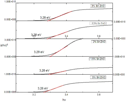
The variation of (αhν)² as a function of the photon energy hν of the pure and Sn doped ZnO are sketched in Fig.3 the optical band gap for as-grown films is obtained by the intercept of the straight line on the horizontal axis.
2.1
optical properties
Fig 3: plot of (αhν)² vs hν of pure ZnO and doped Sn
2.2
structural properties
The cristallinity and the preferred crystal orientation of the undoped and Sn doped ZnO films were analyzed by XRD method by Bruker D8 ADVANCEwith DAVINCI design diffractometer as shown in Fig.4
Films Sn/Z
n (%)
2θ
(°) (°) d (A°)
Cristani llity (%)
Grain Size (nm)
0 33.48 0 2.65 31.1% 14.84
1.5 34.00 -0.52 2.60 45.9% 7.37
2 33.27 0.21 2.70 28.3% 9.19
2.5 33.36 0.12 2.68 42.3% 11.33
3 33.01 0.47 2.71 14.4% 9.81
Fig.4: XRD spectra of undoped and Sn doped ZnO
Fig.4 shows that the films are polycrystalline with a hexagonal wurtzite type structure (ASTM 89-1357). And shows a high diffraction intensity for (002) peak hence the films exhibit preferential orientation along the (002) plane.
The lattice spacing, Bragg angle and percentage of cristallinity and the angle shift is determined as 2 (pure ZnO)-2(doped ZnO) are listed in table 2.
The first peak located at ~22o corresponds to amorphous carbon comes from zinc acetate (Zn (CH3COO)2, 2H2O), amorphous carbon’s peak is sited in Zhou Kong’s work [25]
The lattice spacing was calculated by the Bragg law [3]:
n
λ
= 2 d sin
θ
(1)Where θ is half of Bragg angle, d is the lattice spacing, n is diffraction order and is the X-ray wavelength.
The grain sizes were calculated by Scherer’s formula:
G= (0.94 λ) /β Cos θ (2) Where β is the full width at half maximum.
Fig.5: show the grain size versus doping Sn
Fig.5 show the graphs of cristallinity and grain size versus percentage of Sn as dopant
If we take undoped ZnO film as an example we can say that the film is 31.1% crystallized in groups of grain size ±14.84 nm.
We observe that the grain size of doped ZnO 2% and 3% films is bigger than 1.5% 2.5% films with lower cristallinity as table 2 shown , its maybe due to the influence of thickness of films and/or the influence of the lattice spacing d(A°). The cristallinity increase with decreasing of lattice spacing as it’s shown in Fig.6.
Fig.6: plot of cristallinity, lattice spacing versus doping Sn
2.3
Electrical properties
The current-voltage (I-V) measurements of all films have been carried out by using four-probe method at room temperature (300K), which the sample was held between four gold contacts as sketched in Fig.7.
ZnO has a wide range of electrical conductivity which it can be controlled by doping. The variation of electrical conductivity with doping Sn is shown in Fig.8.
It is shown that the conductivity increase with increasing of doping Sn, it can be explained by the substation of Zn+2 by Sn+4 in ZnO crystal structure which resulting in two more free electron to contribute to the electrical conduction.
Fig.8: plot of electrical conductivity versus doping Sn
Table3 show the electrical parameters as bulk density, mobility, resistivity, hall coefficient.
Sn/Zn %
Nb
(cm-3) µ (cm²/Vs) ρ (Ω.cm) RH (cm3/C) Type VH sign
0 -7.54E12 35.36 2.34E4 -8.276E5 n negative
1.5 3.627E15 15.85 1.086E2 1.721E3 p positive
2 -1.47E16 8.215 51.64 -424E2 n negative
2.5 -2.95E17 2.312 9.149 -21.15 n negative
3 1.064E18 3.67 1.599 5.869 p positive
2.4
Spectroscopy ellipsometry
Spectroscopy ellipsometry (SE) known for its precision and non-destructive, by measuring the change in the light polarization stat as psi (ψ) and delta (Δ) which represent the amplitude ratio and phase difference between p- and s-polarization respectively of the reflected light off the surface of the film. [10.11.12]
SE was use to measure the optical constant at an incidence angle of 70° as it’s shown at Fig.9 and It’s found that the calculated ψ and Δ are consistent with the experimental data for all films.
The optical constants are very important to designing the optical devises, because of their relation to the electronic polarize-ability of ions and the local field inside materials [12]. Thus it’s important to determine the refractive index (n) and extinction coefficient (k) of the films. The dielectric function can be determinate from the optical parameters (n) and (k) by:
ε
1 = n² - k² (3)ε
2 = 2nk (4)Fig.11 show (n) and (k) of the rest of films which has same reaction with doping Sn.
Fig.12 and Fig.13 show the variation of the real and imaginary values of dielectric function.
We observe that we have the same values of ε1 for all films,it means that the films of pure and
Sn-doped ZnO films have the same real part of the dielectric function.
The imaginary part of the dielectric function are shown in Fig.13 which we can observe the reaction of dielectric function with Sn-doping.
Fig.12: real part of dielectric function of undoped and doped ZnO
Conclusion
The impact of tin doping on optical, structural, electrical and spectroscopy ellipsometry of Zinc oxide by ultrasonic spray pyrolisys deposition are investigated.
The optical parametre shows that the films of undoped and doped ZnO are highly transparent and the band gap energy was shifted from 3.26eV to 3.28eV by Burstein-Moss effect due to the introduction of Sn impurty which leads to.
The structural caracterization reveald that the films prefer plan (002) as a preferentiel orientation with best cristanillity is for ZnO doped Sn a 1.5%. which is due to the lowest value of spacing lattice.
The electrical studies show the possibility to get p-type zinc oxide and reveals that the decrease of resistivity due to the increase of the bulk density.
Spectroscopy ellipsometry reveal the optical parameter of ZnO and show that the refractive index decrease with doping increase and that’s due to the change of structure of ZnO by introduction of Sn as impurty. The data of SE reveal that the doping doesn’t affect the real part of dielectric function but the imaginary.
Acknowledgements
The work is included in the PNR project under contract number 8/U311/R77,supported by “agence thématique pour la recherche scientifique et technologique” (ATRST) http://www.atrst.dz, and national administration of scientific research (NASR) www.nasr.dz. This work is a part of CNEPRU project n° D01920120039 supported by Oran university of sciences and technology USTO-MB. The first and second authors are grateful for the assistance of Dicle University-Diyarbakir-Turkey, Mentouri University of Constantine and the virtual library of SNDL https://www.sndl.cerist.dz
References
[1]Shalaka C. Navale, I.S. Mulla, Materials Science and Engineering C 29 (2009) 1317–1320.
[2]M.M.Islama, S. Ishizuka, A. Yamada, K. Matsubara, S. Niki, T. Sakurai, K. Akimoto, Applied Surface Science 257 (2011) 4026–4030.
[3]Jun-ichi Nomoto, Tomoyasu Hirano, Toshihiro Miyata, Tadatsugu Minami, Thin Solid Films 520 (2011) 1400–1406.
[4]M. Benhaliliba • C. E. Benouis, A. Tiburcio Silver, Journal of Technology and Materials JNTM vol.01, N°00(2011) 24-28.
[5]Peng Hu, Ning Han, Dangwen Zhang, Johnny C. Ho, Yunfa Chen, Sensors and Actuators B 169 (2012) 74– 80.
[6]V. Ghafouri, M. Shariati, A. Ebrahimzad, Scientia Iranica F (2012) 19 (3), 934–942.
[7]S.J. Henley, M.N.R. Ashfold, D. Cherns, Surface and Coatings Technology 177 –178 (2004) 271– 276.
[8]M. Benhaliliba • C. E. Benouis • M. S. Aida • F. Yakuphanoglu • A. Sanchez Juarez, J Sol-Gel Sci Technol (2010) 55:335–342.
[9]Y.H. Hwang, H.M. Kim, Y.H. Um, H.Y. Park, Materials Research Bulletin 47 (2012) 2898–2901.
[10]T.W.H. Oates, H. Wormeester, H. Arwin, Progress in Surface Science 86 (2011) 328–376.
[11]Gregory J. Exarhos, Aimee Rose, Charles F. Windisch Jr, Thin Solid Films 308–309 (1997) 56– 62.
[12]Á. Németh, Cs. Major, M. Fried, Z. Lábadi, I. Bársony, Thin Solid Films 516 (2008) 7016–7020.
[13]M. Benhalilba, C.E. Benouis, M.S Aida , A.Sanchez Juarez, F. Yakuphanoglu, A. Tiburcio-Silver, J. Alloys Compds, 506(2010)548-553.
[14]C.E. Benouis, M. Benhalilba, J.Sanchez, M.S Aida, F. Chami,f. Yakuphangulo, J.Alloys and Compds, 490(2010)62-67.
[16]Paul. GK, Sen. GK, optical properties of some sol gel-derived gallium doped ZnO, materials letters 2002; 57:959-63.
[17]Bengisu Ergin, Elif Ketenci, Ferhunde Atay , international journal of hydrogen energy 34 (2009)5249–5254.
[18]Qing Hua Li, Deliang Zhu, Wenjun Liu, Yi Liu, Xiao Cui Ma, Applied Surface Science 254 (2008) 2922–2926.
[19]R. Schmidt-Grund, Thin Solid Films 519 (2011) 2777–2781.
[20]H. Neumann, W. Horing, E. Reccius, Thin Solid Films 61 (1979) 13
[21]A. El Hichou, Thin Solid Films 518 (2010) 4150–4155
[22]Lila Raj Dahal, Thin Solid Films 519 (2011) 2682–2687
[23]E. Zaleta-Alejandre, Thin Solid Films 524 (2012) 44–49
[24]Hiroyuki Fujiwara, Spectroscopic Ellipsometry Principles and Applications, ISBN-13: 978-0-470-01608-4 (cloth: alk. paper)