THE DESIGN OF MICROWAVE OSCILLATOR BY
THE METHOD OF NEGATIVE RESISTANCE
Saranya E
Electronics and Telecommunication Engineering, Bharath University, (India)
ABSTRACT
An electronic oscillator is an electronic circuit that produces a periodic, oscillating electronic signal, often a
sine wave or a square wave. Oscillators convert direct current (DC) from a power supply to an alternating
current signal. A lower phase-noise of the oscillator means less interference between channels and that a
smaller frequency band is needed for the same data rate. For high frequency systems, power output level and
efficiency are always meaningful for reducing amplifier demands and extending the battery life of mobile
systems. Microwave oscillator was selected because their wide use in commercial, space and defence systems
where demanding performance, high reliability and cost are critical. This products take advantage of the small
size, low phase noise and high efficiency with the help of low phase noise amplifiers and Dielectric Resonators.
Low noise oscillators make systems utilize channels more effectively. For the requirement of low
phase-noise, a GaAs FET amplifier was used as the active device for its low phase –noise and high performance at
microwave frequency of 2.5. GHz.
Keywords: Low Phase Noise, Microwave Oscillator, High Quality Factor, Simulation, Negative
Resistance.
I. INTRODUCTION
In this paper we deal with the low phase noise in microwave oscillator. The phase noise of the oscillator is
achieved by increasing the loaded quality factor. Here we use Advanced System Design software to achieve the
simulation. The Bipolar Transistor circuit is selected to perform the simulation of the oscillator. In this note, the
design on a 2.5 GHz bipolar oscillator by the method of negative resistance is used.
II. HEADINGS
In the negative resistance oscillator design, the negative resistors can be realized easily by a three terminals
The figure above (Fig. 1) shows a typical negative resistance oscillator. First, it is necessary to make sure the
overall circuit to be unstable such that:
RIN RL 0 …………..(1)
When a stable oscillation occurs, the following conditions must be satisfied:
RIN RL 0 ……….….(2)
X IN X L 0 ………….(3)
Base on the theory above, a negative resistance will be designed and simulated in ADS to satisfy equation (1)
and a resonator will be designed and simulated in ADS to satisfy equation (2) and (3).
Finally, the combined circuit will be simulated in ADS by the method of harmonic balance to see the overall
performance the oscillator.
II. IDENTATIONS AND EQUATIONS
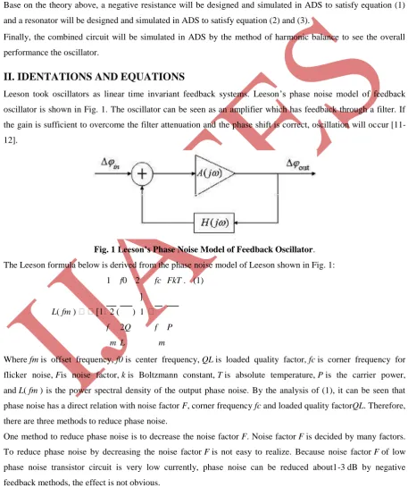
Leeson took oscillators as linear time invariant feedback systems. Leeson’s phase noise model of feedback
oscillator is shown in Fig. 1. The oscillator can be seen as an amplifier which has feedback through a filter. If
the gain is sufficient to overcome the filter attenuation and the phase shift is correct, oscillation will occur
[11-12].
Fig. 1 Leeson’s Phase Noise Model of Feedback Oscillator.
The Leeson formula below is derived from the phase noise model of Leeson shown in Fig. 1:
L( fm ) [1
1 f0 2
fc FkT . (1)
( ) ] 1 f 2 2Q f P m m L
Where fm is offset frequency, f0 is center frequency, QL is loaded quality factor, fc is corner frequency for
flicker noise, Fis noise factor, k is Boltzmann constant, T is absolute temperature, P is the carrier power,
and L( fm ) is the power spectral density of the output phase noise. By the analysis of (1), it can be seen that
phase noise has a direct relation with noise factor F, corner frequency fc and loaded quality factorQL. Therefore,
there are three methods to reduce phase noise.
One method to reduce phase noise is to decrease the noise factor F. Noise factor F is decided by many factors.
To reduce phase noise by decreasing the noise factor F is not easy to realize. Because noise factor F of low
phase noise transistor circuit is very low currently, phase noise can be reduced about1-3 dB by negative
feedback methods, the effect is not obvious.
Another method to reduce phase noise based on Leeson model is to decrease corner frequency fc. The corner
needed to greatly improve integrated circuit technology level, and its influence on phase noise cannot be
reduced effectively using the method of external circuit. Now low noise bipolar transistor's corner
frequency fc generally has fallen to 3-5 KHz. If fc is decreased to 1-2 KHz, near carrier frequency phase noise
can be reduced about 2 dB, the effect also is not obvious.
The third method is to reduce phase noise by improving loaded quality factor QL. The quality factor actually
indicates phase noise characteristics. It not only affects the structure of the phase noise spectral density, but also
affects the intensity of phase noise. Improving unloaded quality factor is restricted by physics and materials.
From (1), we can draw a conclusion that near carrier frequency phase noise improves with increasing QL. So a
high QL is beneficial to reducing near carrier frequency phase noise.
Based on above analysis, we can draw a conclusion that QL is the main effect factor of phase noise, so it is
feasible to reduce phase noise by improving QL.
2.1
Biasing Circuit
Before we start the design, a suitable transistor should be selected and provided a suitable dc bias (Fig.6). In this
design, the Agilent Technologies High Performance Isolated Collector
Silicon Bipolar Transistor HBFP0450 will be used. It will be biased to operate at 2V VCE and 20mA IC. The
model of the transistor used in the simulation can be found in ADS component library (Fig. 5). In this
simulation, the DC simulator in ADS is used to make sure the required biasing condition is obtained.
2.2 Negative Resistance
After designed the biasing circuit, the transistor will be constructed as a common emitter capacitive feedback
circuit. This will produce a negative resistance in order to cancel the lost from the resonator. In this simulation,
the S-Param simulator in ADS is used of the circuit. From the simulation result, it shows that the overall
resistance of the circuit is zero near 2.5 GHz and satisfies the equation 2.
2.3 S-Parameter (S_Param) Simulator
The S_param simulator is used to find the circuit parameters such as s-, z- and y- parameters. The start and stop
frequency of the wanted parameter is required by the simulator (Fig. 3). Besides, a circuit termination should be
added in the circuit schematic as the measurement port of the circuit. It is used to find the input impedance of
the active device in the negative resistance design and used to check the three oscillation condition equations in
the resonator design.
Fig. 3 S_param simulator
2.4 Harmonic Balance (HB) Simulator
The HB simulator is used to simulate the performance of the oscillator. In this simulator, the expected
fundamental frequency is required. Besides, an portcomponent is added in the circuit schematic. The
osc-port should be placed such that it separates the negative- resistance osc-portion of the oscillator from the resonator
portion. The arrow should point in the direction of the negative resistance.
IV. CONCLUSION
In this application note, a typical negative resistance oscillator designed by using the advanced circuit simulator
ADS is resented. By using a powerful simulator, the design time can be greatly reduced and engineers can
achieve circuit performance before the implementation of circuit.