A Computer Method for studying
Junction Depth of SDR IMPATT diode
and a Comparison of its Performance
Based on Different Semiconductor
Materials
L. P. Mishra
Dept. of ECE, ITER,,SOA University, Bhubaneswar, Orissa, India
S. Chakraborty
Dept. of E&TC Engg, BESU, Shibpur, Howrah 711103, W.B., India
M. Mitra
Dept. of E&TC Engg, BESU, Shibpur, Howrah 711103, W.B., India
Abstract
IMPATT is basically a p+n junction diode, reverse biased to breakdown and can generate microwave or rf power when it is properly embedded in a resonant cavity. The structure of an IMPATT diode is either a p+nn+ or an n+pp+. The objective of this paper is to present a computer simulation method based on the mathematical models for 2-step diffusion of Boron in n/n+ silicon epitaxial wafer and to calculate the junction depth thereon. A comparative study has then been made on different performance parameters like frequency, r.f. power output, breakdown voltages and efficiency based on different semiconductor materials like Si, GaAs and GaP. The result of this work can be utilized by the scientists and researchers for the further development of IMPATT diodes in terms of power, efficiency and frequency. Also results reflect a bright future and potential of GaAs and GaP IMPATTS.
Keywords: SDR IMPATT diode, Simulation of diffusion profile, GaAs and GaP IMPATT, Two step diffusion.
1. Introduction
The fabrication of SDR IMPATT diode commences with the process of diffusion of boron as p-type impurities into epitaxial (n on n+) silicon wafers. In 1965, the first SDR IMPATT diode was developed [Johnston (1965)] and Lee et. al. [Lee (1966)] and in the later part of the same year [Misawa (1966)] the small signal analysis of SDR IMPATT was done and it is found that microwave oscillation is possible from this diode. In this fabrication, silicon wafers were n/n+ of diameters 7.62 cm with As-doped substrate (n+ layer) having thickness 385 microns with a resistivity of 0.003 ohm-cm are used. An epi-layer (n-layer) of phosphorous doped having thickness of 4.75 to 5.25 micron, of resistivity 1 ohm-cm have been used as the starting material for fabrication of IMPATT diode. Arsenic doped substrate has been preferred because of its unit misfit factor, higher conductivity leading to lower contact resistance.
2. Fabrication of P+N Junction for Silicon IMPATT Diode
The fabrication of p+n junction is a two-step process – first a low temperature pre-deposition of boron over silicon substrate and the second step is the high temperature drive-in procedure, where the boron atoms will penetrate the silicon wafer.
Pre-deposition
In pre-deposition a thin layer of impurity is deposited at the surface of the sample by constant source diffusion. Pre-deposition process starts with activation of boron nitride (BN) and then a layer of B2O3 is deposited on the
n-side of n/n+ wafer. In the activation process a solid cake of BN of diameter 7.62 cm is introduced into a quartz furnace. Oxygen is allowed to flow over the BN cake at a rate of 2lt/min for 20 minutes at a temperature of 950oC to form a thick oxide layer according to the chemical relation.
4BN+3O2 = 2(B2O3) +N2 ↑
B2O3 is chemically active. It is then taken out and is reintroduced along with an n/n+ epitaxial silicon slice.
During pre-deposition at 950oC, a combine flow of IOLAR grade nitrogen at the rate of 2lt/min is maintained together with the flow of IOLAR grade oxygen at the rate of 0.05lt/min. This process forms a layer of B2O3 on
the n surface of the n/n+ wafer. In the furnace N2 will create an inert atmosphere surrounding thediffusion zone
and flow of O2 ensures formation of pure B2O3 layer.
Drive-in Diffusion
The quartz boat of the furnace containing the silicon wafer and the B2O3 cake is taken out. The furnace is next
set to a diffusion temperature of 1100˚C and then the boat is re-inserted with the Si-wafer having a thin deposited B2O3 layer on n-side of the wafer. During high temperature drive-in process a flow of IOLAR grade
of nitrogen and oxygen are allowed. The reaction that takes place is. 3Si+2 B2O3=3SiO2+4B
These free boron atoms will impinge Si and the depth of penetration depends on the time and temperature for diffusion.
3. Mathematical Model
Drive-in is modeled as [Helmut (1974) and (Nagchowdhury (2001)]
N (x, t) = [Q/A√πDt] exp (-x²/4Dt) (1) Where limited source conditions are modeled by the statement that at start time t=0, an infinitely thin sheet of impurity charge Q is present.
As in this case pre-deposition [Helmut 1974) and (Nagchowdhury (2001)] is followed by drive-in, an ideal pre-deposition process gives rise to a profile N (x, t1) after a time t where
N (x, t1) = N0 erfc [xj/2√(D1t1)] (2)
Where, D refers to the diffusivity during the pre-deposition process. The statement that the concentration for all time t is given by a constant N0 models constant source conditions. The total number of particles Q that have
been introduced into the silicon by this time can be obtained by integrating N (x, t1) within a limit from 0 to ∞
Q = A∫N (x, t1) dx (3)
Substituting N (x, t1) from equation (2), we get;
Q = A∫N0 erfc [x/2√(D1t1)] dx
Consulting the table the integral yields:
Q = 2AN0√ ( D1t1/π) (4)
Now a drive-in is being subsequently performed for a time t2 at a temperature T2 such that the diffusivity is D2.
Practically the drive-in occurs at a high temperature than pre-deposition and thus D2 is always greater than
D1.Now if t1 and t2 are of the same order, then the condition D2t2 » D1t1 is satisfied. If the product D2t2 is much
greater than the product D1t1, then the charge Q can be approximated as a delta function and forms the initial
condition for the drive-in diffusion. Thus, the profile N (x, t2) will be given by substituting the value of Q in
equation (1)
N (x, t2 ) = [2No /π[( D1 t1/D2 t2)]½ exp (-xj²/4 D1 t1) (5)
From this we can solve for the junction depth (xj) by putting N (xj, t1, t2) = NB. This comes out to be: xj = √ (4 D2 t2 ln (No /NB) (2/π) [(D1 t1)/ D2 t2)]½ (6)
4. Program Description
impurity (No), the background concentration (NB) of the semiconductor, the temperature and time for
pre-deposition and drive in as input parameters from the user at the beginning.
In this analysis it has been considered that pre-deposition temperature to be 950˚C and pre-deposition time as 30 minutes.
In general Surface Concentration (N0)/ Background Concentration (NB) = 105
Diffusivity of Boron in Silicon = 25 exp (-3.51/KT) cm2/sec, where K= Boltzmann constant.
4.1 Plot of Junction Depth vs. Drive-in Time and Temperature
For the plot of figure 1, the drive-in time is varied from15 to 60 minutes in steps of 5 minutes and the drive-in temperature is kept fixed at 1075˚C.
In the plot of figure 2, the drive-in temperature is varied from 1050˚C to 1150˚C in steps of 10˚C with a drive-in time at 30 minutes
Fig.1 Plot of junction depth versus drive-in time for Si-SDR IMPATT diode
Fig.2 Plot of junction depth versus drive-in temperature for Si-SDR IMPATT diode
5. Performance Parameters of Silicon SDR IMPATT Diode
As a source the performance parameters of IMPATT oscillator are frequency, power output and efficiency.
5.1 Frequency of Operation
The transit time frequency corresponding to θ=π transit angle is given by
Where vs = saturated drift electron velocity of Si = 107 cm/sec,W = length of the n-layer (typically 5µm), xj =
junction depth
We have simulated junction depth (xj) using computer methods as stated above which depends on the drive-in
time and temperature; so frequency of operation in turn depends upon these parameters. So the plot of figure 3 and figure 4, shows how the frequency of operation varies with drive-in time and temperature.
Fig.3 Plot of frequency versus drive-in time of a silicon-SDR IMPATT diode
Fig.4 Plot of frequency versus drive-in temperature of a silicon-SDR IMPATT diode
5.2 Power Output
The maximum voltage that can be applied across a semiconductor diode is limited by its breakdown voltage, which, for an uniform avalanche region is given by Vm = EmW, where W is the depletion layer width. The
avalanche breakdown process also limits the maximum current that can be carried by the semiconductor diode, because the current in the space-charge region causes an increase in the electric field (from Poisson’s equation). With the maximum field again given by Em, we obtain Im = EmεsvsA/W. Therefore the upper limit on the power
output is given by the product of Vm and Im:
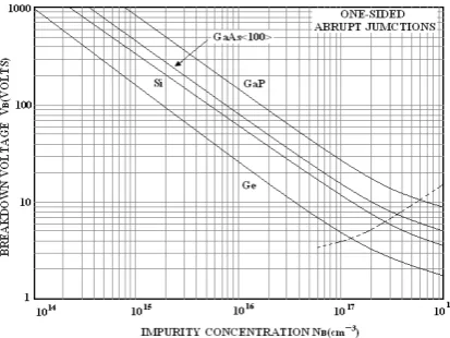
5.3 Breakdown Voltage
Figure.5 shows [Zeghbroeck (2008)] the breakdown voltage and depletion layer width with the change of substrate doping for a planar (top curves), cylindrical (middle curves) and spherical (bottom curves) junction with 1 µm radius of curvature.
Fig.5 Plot of breakdown voltage versus substrate doping
The diffusion parameters and the flow rate of N2 and O2 for different diffusion experiments controls the
substrate doping (of the p+ layer) and hence the breakdown voltage. Hence a control of drive-in diffusion time and temperature can control the substrate doping and hence can fix the breakdown voltage at a desired value for operation of the device at desired range of frequencies.
6. GaAs IMPATT: P+N Junction Fabrication
Cadmium (Cd) diffusion into GaAs single crystals has been investigated in the temperature range 756-1201 °C. Penetration profiles measured by secondary ion mass spectroscopy and spreading-resistance profiling agree with each other and are numerically reproduced on the basis of the kick-out diffusion mechanism. A major involvement of vacancies via the dissociate mechanism can be excluded. This enables us to deduce from the Cd profiles effective Cd diffusivities (Dseff). The Dseff values obtained from As-rich and As-poor ambient are
mutually consistent. Reduced to 1 atm of As vapor pressure and electrically intrinsic conditions the Cd diffusion coefficient results as 5×10⁻² exp (-2.6 eV/kB T) cm2 s-1. However to overcome the low temperature dissociation
characteristic of GaAs a sealed tube diffusion method has been employed, wherein a substrate and a dopant are placed in boats in a tube which is then sealed. Sealed tube diffusion is generally carried out at 750-950°C with arsenic overpressure. The overpressure is employed to prevent dissociation of the arsenic from the substrate.
7. GaP IMPATT: P+N Junction Fabrication
Very smooth planar p+n junctions can be formed in gallium phosphide by the diffusion of zinc into n-type GaP from ZnP2 source.
A process for forming a p+n junction in GaP comprises the steps of enclosing n-type GaP and ZnP2 in
an evacuated chamber and heating the chamber to a temperature of between 800-950˚C for a time sufficient for Zn to diffuse into said n-type GaP so as to form a p+n junction therein.
8. Frequency Consideration of Si, GaAs, and GaP IMPATT Diodes
Table:1
Comparison of the operating frequencies of Si, GaAs and GaP IMPATT for different values of diffusion times and temperatures
Si GaAs GaP
Drive-in time(mins) Frequency (GHz) Drive-in time(mins.) Frequency (GHz) Diffusion time(mins.) Frequency (GHz)
15 2.08 15 3.26 30 2.085
45 8 45 16.23 45 7.76
50 12.3 50 32.5 50 62.5
53 18.1 53 76 53 80
55 25.9 55 138 55 150
Drive-in temperature (˚C) Frequency (GHz) Drive-in Temperature (˚C) Frequency (GHz) Diffusion temperature (˚C) Frequency (GHz)
1050 2.6 850 2.7 800 3.7
1080 4.2 910 6 820 9.6
1095 9.08 920 17.9 830 15.6
1100 15.8 930 76.25 840 125
9. Power Considerations of Si, GaAs and GaP IMPATT Diodes
Using the power frequency relations mentioned earlier in equation (8), a comparison can be made between Si, GaAs and GaP IMPATT diodes as described in table 2.
Table 2
Comparison of breakdown field and saturated drift velocity of Si, GaAs and InP IMPATTs
Si GaAs GaP
Breakdown field Em(106 V/cm)
(@ ND = 1017 cm-3)
0.61 0.65 0.937
Saturated electron drift velocity vs(10 7
cm/sec)
(@ E > 5*105 V/cm)
1 0.6 1.25
10. Breakdown Voltages for Si, GaAs and GaP IMPATT Diodes
For one-sided abrupt junctions as a p+n junction in IMPATT
VB = EmW/2 = εsEm2/ (2qNB) (9)
Where NB is the ionized background impurity concentration of the lightly doped side, εs the semiconductor
permittivity and Em the maximum field. Now a plot of breakdown voltage versus impurity concentration is
shown [Sze (1981)] in figure 6.
11. Calculation of Efficiency
The microwave power generating efficiency η = ac power output/ dc power input =(2J0/π) (mVD)/ ( J0(VA+VD))|cosφ|
= (2m/ π)[1/(1+VA/VD)] |cosφ|
Where VA is the dc voltage drop across the avalanche region and the sum of VA and VD is the total applied dc
voltage. The angle φ is the injection phase delay of particle current. Under ideal conditions φ is 180˚ and |cos φ|=1.
Thus in order to improve frequency one has to increase the ac voltage modulation factor, optimize the phase delay angle toward 180˚ and reduce the (VA/VD) ratio. However VA must be sufficiently large to initiate
the avalanche process rapidly.
If the velocity field relation for the drifting carriers were such that the velocity was saturated at very low electric fields, m would approach unity and no falling out of velocity saturation would occur. In n-type Si, the velocity is effectively saturated near 2×10⁴ V/cm.
For f = 10GHz, the optimum value of VA/VD for GaAs is 0.65 with m=1, while for Si the optimum
value is about 1.1 with m = ½.
The maximum efficiency is obtained using the optimum values discussed above. A comparison is made in terms of efficiency for Si, GaAs and GaP IMPATT diode as described in table 3.
Table 3
Comparison of efficiencies of Si, GaAs, and GaP IMPATT diodes IMPATT Diode material Maximum efficiency
Si 15% (SDR)
GaAs 38% GaP 40% 12.0 Conclusion
Here a detailed analysis is made with the mathematical model using MATLAB to simulate the effects of diffusion parameters on the junction depth, frequency of operation, power output and efficiency of the Si-SDR IMPATT diode as well as GaAs and GaP IMPATT diodes and the results are compared to those obtained experimentally.
GaAs have higher frequency of operation for lower diffusion times and temperatures, whereas GaP having a high value of critical field reported high values of power for high frequencies. But because of simplicity, low processing cost and easy availability silicon IMPATT diodes are fabricated and used mostly.
GaP diodes exhibit frequencies as high as in the V-band (50-75 GHz) and W-band (75-110 GHz) for diffusion time comparable to that of Si and GaAs and for diffusion temperature much lower than that of Si. The high frequencies in GaP may be attributed to a higher value of the saturated electron drift velocity.
Maximum electric field in GaP is about 53% larger than that of Si while vs is 25% larger than that of
Si. Therefore, GaP IMPATT diodes are expected to have a power output 3.65 times larger than that of a Si IMPATT operated at the same frequency.
References
[1] R.L. Jhonston, B.C. De Loach Jr. and B.G.Cohen., (1965) “A Silicon Diode Microwave Oscillator”, Bell system Technology Journal,
Vol. 44, No. 2, p.401-446”.
[2] C.A. Lee, R.L. Batdorf, W. Weightmann and G. Kaminsky, (1966) “ Technological Development Evolving From Research on Read
Diodes” IEEE Trans. on Electron Devices, vol. ED-13, No.1, p. 175-180
[3] T. Misawa, (1966) “Negative Resistance in p-n junction under avalanche breakdown conditions – part 1 and 2”,IEEE Trans on
Electron Devices, vol. 13, No. 1,p. 137-151.
[4] Helmut Wolf, (1974) “Hand book of Semiconductors”, John Wiley & Sons Inc., NY.
[5] D. Nagchowdhury, (2001) “Principle of Microelectronic circuits”, Wheeler Publishers, New Delhi.
[6] Bart Van Zeghbroeck, (2008) “Principles of Semiconductor Devices”, Prentice Hall, 1st edition,
(http://ece-www.colorado.edu/~bart/book/book/chapter4/ch4_5.htm).