Implementation of BIST Structure using
VHDL for VLSI Circuits
Mrs.Jamuna.S,
Asst Professor, Department of ECE, DSCE,
Bangalore
Dr. V.K. Agrawal
Group Director, ISRO,
Bangalore
Abstract-- Very Large Scale Integration (VLSI) has made a dramatic impact on the growth of integrated circuit technology. It has not only reduced the size and the cost but also increased the complexity of the circuits. The positive improvements have resulted in significant performance/cost advantages in VLSI systems. There are, however, potential problems which may retard the effective use and growth of future VLSI technology. Among these is the problem of circuit testing, which becomes increasingly difficult as the scale of integration grows. Because of the high device counts and limited input/output access that characterize VLSI circuits, conventional testing approaches are often ineffective and insufficient for VLSI circuits. Built-in self-test (BIST) is a commonly used design technique that allows a circuit to test itself. BIST has gained popularity as an effective solution over circuit test cost, test quality and test reuse problems. In this paper we are presenting an implementation of a tester using VHDL.
Key words: BIST, LFSR, MISR.
I. Introduction:
Test time is a significant component of IC cost. It needs to be minimized and yet has to have maximum coverage to ensure zero-defect. The goal of testing is to apply a minimum set of input vectors to the device to determine if it contains a defect. Costs increase dramatically as faulty components find their way into higher levels of integration[1]. Thus, there is a need for design for testability techniques.
For any testing methodology, the following factors should be considered- high and easily verifiable fault coverage, minimum test pattern generation, minimum performance degradation, at-speed testing, short testing time, and reasonable hardware overhead[2]. Built-In Self-Test (BIST) provides a feasible solution to the above demands. First, BIST significantly reduces off-chip communication to overcome the bottleneck caused by the limited input/output access. Further, it eliminates much of the test pattern generation and simulation process[2]. Testing time can be shortened by testing multiple units simultaneously through test scheduling. Hardware overhead can be minimized by careful design and through the sharing of test hardware.
In the modern System-on-a-Chip (SoC) design, many cores are integrated into a single chip. Some of them are embedded, and cannot be accessed directly from the outside of the chip. Such SoC designs make the test of these embedded cores a great challenge[1]. BIST is one of the most popular test solutions to test the embedded cores. Another advantage of this methodology is that the test patterns are not applied by external Automatic Test Equipments (ATEs) but generated by inbuilt testing circuit. It saves the memory requirement during test. The remainder of this paper is organised as follows. Section II gives an explanation about BIST concept. Section III describes mathematical analysis of the concept. Section IV gives an illustration of fault detection process, section V describes simulation results. Section VI concludes the paper.
II. Built-in self-test (BIST)
The commonly seen test strategies are,
1. Stored Patterns: Stored-pattern approach stores the pre-generated test patterns to achieve certain test goals. It is often found in system level testing such as the power-on self test of a computer and microprocessor functional testing using micro programs[3].
2. Exhaustive Testing: Exhaustive testing applies all possible input combinations to the circuit under test (CUT). It guarantees that all detectable faults that do not produce sequential behavior will be detected. The strategies are often applied to complicated and well isolated small modules such as PLAs [4].
3. Pseudorandom Testing:
4. Weighted Pseudorandom Testing: Weighted pseudorandom testing applied pseudorandom patterns with certain 0s and 1s distribution to handle the random pattern resistant faults undetectable by the pseudorandom testing. It can effectively shorten the test length.
5. Pseudo exhaustive Testing: Pseudo exhaustive testing partitions the CUT into several smaller sub circuits and tests each of them exhaustively. All detectable faults within the sub circuits can be detected. However, such a method requires extra design effort to partition the circuits and deliver the test patterns and test responses.
BIST is a set of structured-test techniques for combinational and sequential logic, memories, multipliers, and other embedded logic blocks. BIST is the commonly used design technique that allows a circuit to test itself.
Principle of BIST: Generate test vectors, apply them to the circuit under test (CUT) or device under test (DUT), and then verify the response [1].
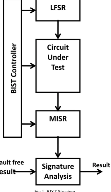
Fig 1. BIST Structure
Fig.1 shows a simple BIST block diagram which uses a linear feedback shift register (LFSR) to generate the test vectors and multiple input signature register (MISR) to verify the output against the correct response of the circuit under test.
Linear Feedback Shift Register
LFSR is an n-bit shift register which pseudo-randomly scrolls between 2n-1 values, but does it very quickly because there is minimal combinational logic involved [2]. The all zeros case is not possible in this type of LFSR, but the probability of any bit being "1" or "0" is 50% except for that. Therefore, the sequence is pseudorandom in the sense that the probability of a "1" or "0" is approximately 50%, but the sequence is repeatable. Like a binary counter, all 2n - 1 states are generated, but in a “random” order that is repeatable. The exclusive-OR gates and shift register act to produce a pseudorandom binary sequence ( PRBS ) at each of the flip-flop outputs. By correctly choosing the points at which we take the feedback from an n -bit shift register we can produce a PRBS of length 2n – 1, a maximal-length sequence that includes all possible patterns (or vectors) of n bits, excluding the all-zeros pattern.
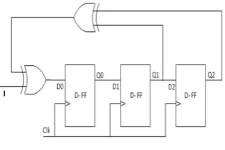
In an LFSR, the bits contained in selected positions in the shift register are combined in some sort of function and the result is fed back into the register's input bit. Fig.2 shows a 3bit LFSR.
LFSR
Circuit
Under
Test
MISR
BIS
T
Con
tr
o
ller
Signature
Analysis
Fault
free
Fig 2. 3-bit maximal-length LFSR
Feedback around an LFSR's shift register comes from a selection of points (taps) in the register chain and constitutes XOR ing these taps to provide tap(s) back into the register.
Clock
tick
Q0 t+1
= Q1
t
ْ
Q2 t
Q1 t+1
= Q0
t
Q2 t+1
= Q1
t
Q0Q1Q2
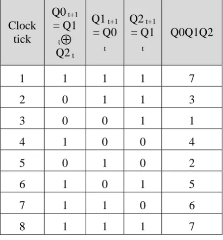
1 1 1 1 7
2 0 1 1 3
3 0 0 1 1
4 1 0 0 4
5 0 1 0 2
6 1 0 1 5
7 1 1 0 6
8 1 1 1 7
Table .1 Maximal-length sequence for the 3-bit LFSR in above figure
Register bits that do not need an input tap, operate as a standard shift register. It is this feedback that causes the register to loop through repetitive sequences of pseudo-random value[2]. The choice of taps determines how many values there are in a given sequence before the sequence repeats. The implemented LFSR uses a one-to-many structure, rather than a many-to-one structure, since this structure always has the shortest clock-to-clock delay path.
The feedback is done so as to make the system more stable and free from errors. Specific taps are taken from the tapping points and then by using the XOR operation on them they are feedback into the registers.
Signature Analysis
MISR - Multiple-Input Signature Register
A input signature register can only be used to test logic with a single output. The idea of a serial-input signature register can be extended to multiple-serial-input signature register ( MISR ). There are several ways to connect the inputs of LFSRs to form an MISR[7]. Since the XOR operation is linear and associative, ( Aْ B)
ْ C = A ْ (B ْ C ), as long as the result of the additions are the same then the different representations are equivalent. If we have an n -bit long MISR we can accommodate up to n inputs to form the signature. If we use m < n inputs we do not need the extra XOR gates in the last n – m positions of the MISR. MISR reduce the amount of hardware required to compress a multiple bit stream. LFSR and/or MISR circuit is implemented using a memory already existing in a circuit to be tested.
Fig 3.MISR with 3 input and 3 output bits
III. Mathematical Analysis
If we apply a binary input sequence to LFSR, the shift register will perform data compaction (or compression ) on the input sequence. At the end of the input sequence the shift-register contents, Q0Q1Q2 , will form a pattern that we call a signature . If the input sequence and the serial-input signature register ( SISR ) are long enough, it is unlikely (though possible) that two different input sequences will produce the same signature.
If the input sequence comes from logic that we wish to test, a fault in the logic will cause the input sequence to change. This causes the signature to change from a known good value and we shall then know that the circuit under test is bad. This technique, called signature analysis, was developed by Hewlett-Packard to test equipment in the field in the late 1970s. The simplest form of this technique is based on a single input LFSR.
Fig. 4 A 3-bit serial-input signature register (SISR)
Every LFSR has a characteristic polynomial that describes its behavior. Degree of polynomial is given by the number of shift registers. Ex: for the fig shown, the characteristic polynomial is given by P(x)=1+x2+x3 . The characteristic polynomial that causes an LFSR to generate maximum length PRBS are called primitive polynomial[8]. Consider LFSR with characteristic polynomial given as P(x)=1+x2+x3 .
Consider CUT be Y=AB+BC. The o/p of the CUT (good condition)for the LFSR pattern {7,3,1,4,2,5,6,7} is given as {1,1,0,0,0,0,1,1} and the corresponding polynomial is given by
G(X) = 1+X+X6+X7.
The o/p of the CUT (bad condition i.e with s-a-1-fault at B i/p line )for the lfsr pattern {7,3,1,4,2,5,6,7} is given as {1,1,1,1,0,1,1,1} and the corresponding polynomial is given by
G(X) = 1+X+X2+X4+X5+X6+X7.
X3+X+1 X7+X6+X+1
X7+X5+X4
X6+X5+X4+X+1
X6+X4+X3
X5+X3+X+1
X5+X3+X2
X2+X1+1
Remainder X2+X1+1 corresponds to signature 111.
IV. Fault detection using MISR - Illustration
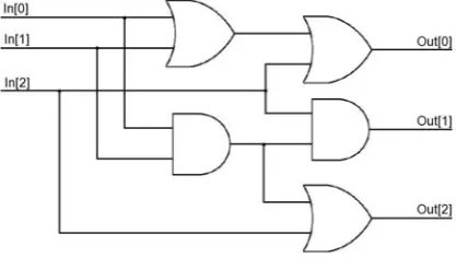
Consider the circuit shown in figure. The circuit can be expressed using Boolean equation as,
Out[0] = In[0] + In[1] + In[2]
Out[1] = In[0] . In[1] . In[2]
Out[2] = ( In[0] . In[1] ) + In[2]
We have three input bits and three output bits for the given circuit to be tested. So we design an LFSR with three output bits to generate the test vectors. Let the LFSR be of maximal length so that we get the test vector sequence or pseudo random binary sequence as {111, 011, 001, 100, 010, 101, 110} as explained earlier. This pseudo random binary sequence is applied to the circuit under test and the output is recorded. The output at the end of 7th clock is taken as the signature.
Clock tick
LFSR
output
Output
of
circuit
under
test
MISR
Outputs
Signature
1 111
111
000
110
2 011
101
111
3 001
001
000
4 100
101
001
5 010
001
111
6 101
101
100
7 110
101
110
Table. 2 Response for fault free circuit
From the table we can see that the signature value is 110 for a fault free circuit.
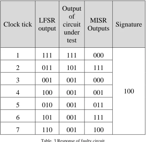
Now consider the circuit in the presence of a fault. Let the circuit has a stuck at zero(s-@-0) fault at the input of the OR gate for the computing outbit.
For the 4th clock tick the faulty circuit gives incorrect output. But for the 5th clock tick the output is same in the presence and absence of fault, but the multiple input signature register output remain different ever after the first occurrence of the fault. Also when the complete pseudo random binary sequence is applied to the circuit under test, ie at the end of 7 clock ticks, we take the output of signature register as the signature of the circuit under test.
Clock tick
LFSR
output
Output
of
circuit
under
test
MISR
Outputs
Signature
1 111
111
000
100
2 011
101
111
3 001
001
000
4 100
001
001
5 010
001
011
6 101
001
111
7 110
001
100
Table. 3 Response of faulty circuit
We can see that the signature values computed for correct and faulty circuit are different. Hence we can conclude that verifying the signature of a circuit, on applying the complete pseudo random binary sequence, to the signature value computed earlier or generated by a fault free circuit is sufficient to determine whether the circuit is faulty or operating correctly. The MISR propagates the fault from the clock cycle where it appeared first till the end of the input sequence with the help of the feedback.
The test pattern can be repeated after resetting the multiple input signature register. When the test pattern is repeated, the responses remain the same as long as the fault is present. When fault is detected in an IC right after manufacturing, we can easily remove it. But if the fault is to be detected after integrating the IC to a PCB, the cost of finding the fault as well as correcting it is higher. This cost keeps increasing as the fault detection stage is later in the production procedure.
V. Simulation results of VHDL implementation
For the 4th clock tick the faulty circuit gives incorrect output. As the input is stuck at zero, we get a corresponding faulty zero output for bit(2).
Fig. 8 Incorrect output from the faulty circuit
For the 5th clock tick the output is same in the presence and absence of fault, but the multiple input signature register output is different ever after the first occurrence of the fault. Also when the complete pseudo random binary sequence is applied to the circuit under test, ie at the end of 7 clock ticks, we take the output of signature register as the signature of the circuit under test.
Fig. 9 MISR output, Signature and fault detection
Fig. 10 Response to the complete test sequence (Initial)
Fig. 11 Response to the complete test sequence (Repeated)
Figure shows the response of the circuit under test (reference and faulty), MISR, Signature calculation and fault detection. When the test pattern is repeated, the responses remain the same.
VI. Conclusion.
In this paper we have illustrated an implementation of BIST logic using VHDL. LFSR is used as a pseudorandom sequence generator. Signature analysis is used to make verification of the circuit. Signature mismatch with the reference signature means that the circuit is faulty. However, there is a small probability that the signature of a bad circuit will be the same as a good circuit. When longer sequences are used , signature analysis gives high fault coverage.
References
[1] M.Bushnell and V.D. Agarwal, “ Essentials of Electronic Testing for Digital, Memory and Mixed-signal VLSI Circuits” Kluwer Academic Publishers, 2000.
[2] Digital system testing &testability. Abromovici
[3] M.S. Abadir and M.A. Breuer, “A knowledge – based system for designing testable VLSI chips,” IEEE Design & Test of Computers, Vol. 2, no.4, Aug 1985, pp 56-68.
[4] V.D. Agrawal, C.R. Kime and K.K. Saluja, “ A tutorial on BIST part1: IEEE Design & Test of Computers, March 1993, pp 73-82.
[5] P.H. Bardell, W.H.McAnney and J. Savir, Built-in test for VLSI: Pseudorandom Techniques, John Wiley & Sons, Newyork, 1987.
[6] L.T. Wang, Cheng- Wen Wu and Xiaoqing Wen, “ VLSI Test Principles & Architectures Design for testability”. [7] M.J. Smith, “Application Specific Integrated Circuits”.