Implementation of Communication Protocols
in FPGA for Testing of Microcontrollers
Betty George1,Tina Raja2
PG Student [Applied Electronics], Dept. of ECE, MG University College of Engineering, Thodupuzha, Kerala, India1
Scientist/Engineer "SE", QDAC/QRAG/SR/ VSSC, Trivandrum, Kerala, India2
ABSTRACT: Communication between devices is made possible by various protocols. Among them are UART and
SPI. This paper proposes a novel approach in the implementation of UART and SPI protocols in Field Programmable Gate Array. A memory module is also used which serves as a temporary storage. The SPI protocol implemented works in four different selectable frequencies. The UART is an asynchronous data transmission protocol with an in built baud rate generator. The proposed system could be used for the exchange of data between devices that posses any one of the above specified mode of communication. Hence this implementation is useful for testing of microcontrollers. The implementation of the protocols is done using HDL in ModelSim platform and synthesis in Xilinx platform.
KEYWORDS: Communication Protocols, FPGA, UART, SPI, HDL implementation.
I.INTRODUCTION
UART has its abbreviation as Universal Asynchronous Receiver Transmitter. UART can be used to establish transmission between fast and slow peripherals and thus it is used in low speed, low cost and short distance applications. UART mainly consist of transmitter, receiver, baud rate generator and memory. At the transmitter end, the data is converted from parallel to serial form and at the receiver end; received data in serial form is converted to parallel form .UART interface chip could apply various serial bus interface standards such as RS-232, RS-422 and RS-485. Anyhow there are devices with either any one of the above specified interface.
Serial Peripheral Interface is a serial communication protocol. It establishes a full duplex path between the communicating devices and is employed for inbox or short range applications. It mainly consists of two blocks; SPI master and SPI slave. SPI protocol defines four signal connections; MISO (master in slave out), MOSI (master out slave in), SS (slave select) and SCLK (serial clock). In most of the microcontrollers used the frequency at which the master works is selectable; Fosc / 4, Fosc / 16 etc. This particular scenario is considered in this paper.
The protocols are developed for the testing of microcontrollers. The device under test is PIC18F65XX microcontroller, which has various communication modules which are to be tested including UART and SPI. The communication to the test station is also through UART (RS 232). Through the implementation of these protocols in FPGAs, interface between the device under test (DUT) and test station is achieved. Fig.1 shows structure diagram of test system. The SPI and UART interfaces implemented in FPGA are used to test the interfaces of the PIC microcontroller. Also the UART interface is used to communicate with the test station which is usually a standard PC.
As integrated circuit technology is becoming complex, hardware description languages are more in use for the designing of circuits. In this paper, the design implementation is done using VHDL in ModelSim platform. The synthesis is carried out in Xilinx software.
The cutting edge in this implementation of SPI and UART interface is that the interfaces could be used to communicate with devices having any one of the above mentioned interfaces. Also a communication to standard PC through the RS 232 interface could be achieved. Taking into account, the selectable SPI master frequency in case of a microcontroller as master; the proposed interface operates for four different selectable frequencies. The memory implemented serves the purpose of retaining data from the peripheral device if real time application is not the case. It is not mandatory for all devices to have UART as well as SPI interface, thus a computer could communicate with devices having any of the above mentioned interfaces using the proposed device.
II.LITERATURE SURVEY
The implementation of high speed UART using Verilog description language and its synthesis on Virtex4 and Spatan3
FPGA kits has been proposed by Wakhle et al[1]. Some consideration has also been given to implementation of UART
on programmable logic devices in order to realize a communication between DSP which has synchronous serial ports and devices having asynchronous communication protocol has been proposed by Wang et al [2]. The bit error rate test was carried out in the physical system. The GLB used by UART and bit error rate is calculated. RS-422 protocol was
implemented in the paper. All modules were simulated by MAXplusII. Following the work previously reported[3] an
optimal implementation of UART-SPI interface in SOC is done, which could be used to communicate between SPI slave devices and PC. The interface accomplishes the task of interfacing EEPROM’s, flash memories sensors etc. The proposed system considers a microcontroller as target device. The selectable frequency for baud rate and SPI are implemented in the proposed paper. Apart from the memory defined by the protocols, a memory module is implemented for retaining of data obtained from both UART and SPI modules.
III.WORKING PRINCIPLE AND DESIGN
III.A.UART
UART interface module supports the computer with RS-232 data terminal equipment. By this, the computer could transmit as well as receive data from other peripheral devices. UART transmission as well as reception data frame consists of start bit (logic “0”), 5-8 data bits, stop bit (“1”), parity bit (even or odd) and idle state usually logic “1”.When a transmitter starts sending data, it sends logic “0” for a time width of baud rate clock cycle, followed by 5-8 bits of data, and then optional even or odd parity bits are sent. The stop bit mark the ending of the transmission and conveys the message that there is no more data bits in the queue. Fig 2 shows the data frame format of UART.
Fig.2 Data frame of UART
UART has transmitter, receiver and baud rate generator.
UART transmitter has Transmitter Buffer Register and Transmitter Shift Register. The transmitter functions as a parallel to serial converter that takes parallel data and sends serial data. The UART includes two types of registers; hold registers and shift registers. The hold register contains the data that are to be transmitted next while the shift register contains the data that are to be transmitted in the serial manner.
parallel converter, which takes in serial data from the outer peripheral device and stores data in a parallel manner to the memory.
Baud rate generator of UART generates sampling signals with frequency sixteen times that of the designated baud rate. Baud rate indicate the number of signal changes per second
III.A.1 UART TRANSMITTER DESIGN
The basic function of UART transmitter includes addition of start bit and stop bit to the beginning and ending of data (parity bit is absent). Parity bit is provided for the transmitter output and is checked for at the receiver end. Eight bit of value is transmitted in bit by bit manner along with start bit, stop bit and parity bit. In the proposed system, the transmitted values are taken from the memory implemented, where it is stored. It could be transmitted to other peripheral devices according to the need. The basic design diagram of transmitter is shown in Fig.3
Figure.3 UART Transmitter
III.A.2 UART RECIEVER DESIGN
UART receiver receives data from the external peripheral device. Start bit conveys receiver with the message that the data has arrived. Always the start bit is logic “0” value and it is continuously polled. A valid reception is indicated by the start bit. In the proposed system, the received values are copied on to the memory implemented, where it is stored for further usage. It could be transmitted to other peripheral devices according to the application. Fig 4 shows the basic design block of an UART receiver.
Baud rate generator of UART generates sampling signals with frequency sixteen times that of the designated baud rate. Baud rate indicate the number of signal changes per second.
III.B SPI DESIGN
SPI is a high speed synchronous data transmission protocol. SPI mainly include a master and selectable slave devices. The master initiates the communication with slave device and the clock signal is provided by the master device for synchronization. For certain devices such as microcontrollers, the SPI module works at selectable clock frequency. The required frequency is selected by changing the bits that refer to the frequency selection in the corresponding registers of microcontrollers.
SPI protocol is a single master protocol having only one master at a time. When data transfer is initiated, the master sends data through the MOSI line which is read by the slave and at the same time, the slave sends a data through MISO line which is read by the master on every clock cycle SCLK. Thus SPI is a full duplex transmission protocol. When the eighth bit of the master register shits out to the slave shift registers first bit position through the MOSI line, simultaneously the eighth bit of the slave shift register shifts out to the first bit position of the master shift register through MISO line. After eight consecutive clock cycle or shifts, the complete eight bit of data from the master is copied onto the slave shift register and the slave shift register value is copied onto the master register. On every clock cycle there is an exchange of data between the master and slave. The devices could not act as mere transmitter or receiver.
SS signal controls the selection of the slave. SS line is supplied to each and every slave that exists in the circuit. This particular signal indicates the willingness of the master to start a communication with the slave device. SS is an active low line which indicates that SPI is inactive when SS line is in logic 1 state and SPI is active when SS line is in logic 0 state. Fig 4 shows the basic working of SPI module.
Fig.5 SPI Basic Block Diagram
Only the master device manipulates the clock line SCLK. Data transfer occurs only in accordance with the clock provided by master. The clock provided by the master is distributed among the slaves. The slave devices are bound to work in the clock provided by the master. There are provisions for the selection of master clock frequency.
CKE=0, transmission occurs on the transition of clock from idle to active clock state. The CKP bit deals with the polarity of the clock. For CKP=1, the idle state for clock is high and CKP=0, the idle state for the clock is low.
IV.HDL IMPLEMENTATION AND SYNTHESIS
In accordance with the working principle and design of UART, SPI and memory, the combined structure diagram of the implementation is obtained. The combined structure diagram is shown in Fig 5.
Fig.6 UART-Memory-SPI interface diagram
State machines are used to realize the working and functionality of transmitter as well as receiver. Transmitter state machine is shown in Fig.7. There are 11 states in the transmitter state machine. When reset is applied, the idle state is executed and the transmitter waits until for reset is asserted to low. An initiation signal is given to the transmitter. A start bit is polled for and when it is a 0 value, the transmitter moves to the next state after a predetermined baud clock cycle. Then the next eight states indicate the eight data bits. Transmitter changes it state from one to another after the baud clock cycles. A stop bit marks the ending of the data frame and indicates the receiver that the data frame has finished. After the stop state, the transmitter moves to idle state.
Fig.7 State Machine: Transmitter
Fig.8 State Machine: Receiver
DUT taken is a microcontroller PIC18F65XX. The SPI module in microcontroller works in three different frequencies, SPI module implemented works in three different frequencies.SPI module implemented posses a selection line used for the selection of master clock frequency. The clock obtained is changed in accordance with the need using a clock divider. When a bit is received from the slave device, a bit is also transmitted to the slave device at predetermined master clock cycles.
The memory implemented is an array memory with 256 locations and 8 bit wide. Read and Write controls are used. The storing of values into the memory is controlled by the write signal and reading of values from memory is controlled by read signal.
V.RESULT
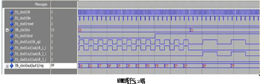
The simulations are done using ModelSim platform. The UART transmitter in Fig.9 takes in data in parallel manner and outputs the data in serial manner. Transmit hold registers and transmit shift registers are implemented which serves the purpose of retaining the data and shifting of data respectively. The transmitted data is taken from the memory implemented. An initiation signal is defined for the transmission purpose.
Fig.9 Transmitter
Fig.10 Receiver
SPI module in Fig.11 shifts out bit in a serial manner at every clock cycle. After eight consecutive clock cycles, the entire eight bit data is shifted to the external device. As the proposed system is serves as the interface between a DUT and test station, one master one slave concept is used. SS signal in this implementation indicates the selectable clock frequency. When SS=”00”, the clock frequency selected is Fosc/4, for SS=”01” clock frequency is Fosc/16 and for SS=”11”, clock frequency is Fosc/64.
Fig.11 SPI
Memory module implemented, Fig.12 serves the purpose of temporary storage of data. Either reading from the memory or writing onto the memory is made possible using control signals. Full and Empty signals denote whether the memory is full or empty. The write control is activated only if the memory module has free space denoted by the write control signal similarly the read control is activated only if the memory module has data in it which is controlled by read control signal.
Fig.12 Memory
Logic Utilization Used Available Utilization
Number of slices 1494 3584 41%
Number of slice flip flop’s 599 7168 8%
Number of 4 input LUT’s 2841 7168 39%
Number of bonded IOB’s 19 141 13%
Number of GCLK’s 2 8 25%
Table 1 Device Utilization
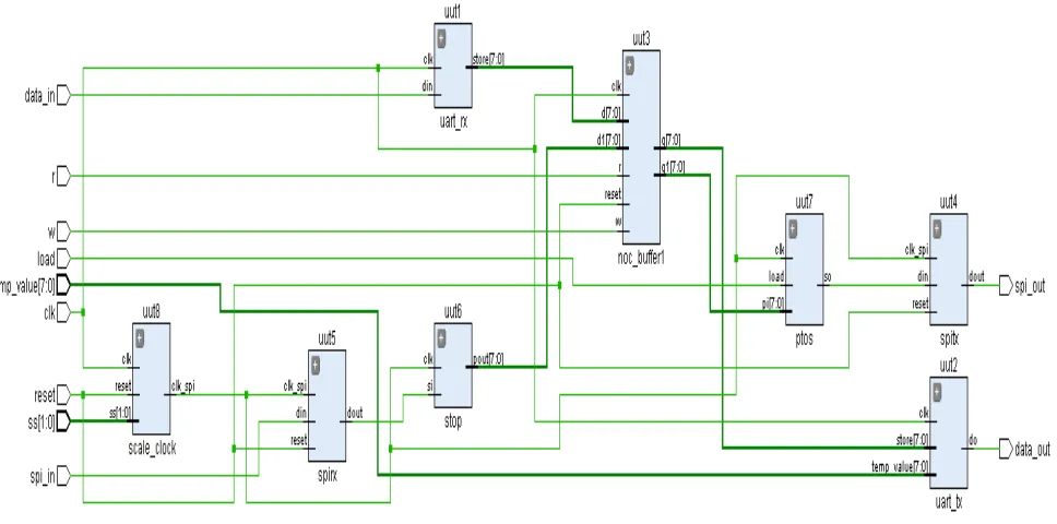
The various blocks implemented are UART transmitter, UART receiver, Memory, Serial to parallel converter (stop), parallel to serial converter (ptos), and SPI module including the clock selection circuit and data shifting section. Read control and write controls are provided. The input to the proposed device is from that of an external device to the UART receiver and from the SPI module. The output is from UART transmitter and the SPI module. RTL schematic in Fig.13 is generated by the Xilinx software during implementation onto the FPGA.
Fig.13 RTL Schematic
VI.CONCLUSION
Extensive simulations were carried out to test the implemented modules. Synthesis report shows the number of slices, LUTs, GCLKs etc used.
REFERENCES
[1] Dr G.B.Wakle, I. Aggarwal and S. Gaba, “Synthesis and Implementation of UART using VHDL Codes”, International Symposium on Computer, Consumer and Control, pp.1-3, June 2012.
[2] Y. Wang and K. Song, “A New Approach to Realize UART,” in Electronic and Mechanical Engineering and Information Technology (EMEIT), International Conference, vol. 5, pp. 2749 –2752, 2011.
[3]T.P.Blessington, B.B.Murthy, G.V.Ganesh and T.S.R Prasad, “Optimal Implementation of UART-SPI Interface in SOC”, Devices, Circuits and Systems (ICDCS), International Conference, pp.673-67, 2012.
[4] S. Yu, L. Yi, W. Chen, and Z. Wen, “Implementation of a Multichannel UART Controller Based on FIFO Technique and FPGA,” in Industrial Electronics and Applications.ICIEA,2nd IEEE Conference, pp. 2633 –2638, 2007.
[5] Motorola Inc., “SPI Block Guide V03.06,” February 2003.
[6] XU L Y, "Realization of UART Communication Based on FPGA” Microcomputer Information, vol. 23(35), pp. 218-219,2007.
BIOGRAPHY
Betty George, received the graduation in Bachelor of Engineering degree in Applied electronics
and Instrumentation from Mar Baselios College of Engineering and technology in 2013, Idukki (Kerala) and is currently PG Scholar at MG University College of engineering in Applied Electronics. Her main areas of interest are Image Processing and VLSI testing.
Tina Raja, received the graduation in Bachelor of Engineering in Electronics and