Copyright to IJAREEIE 10.15662/ijareeie.2015.0402150 801
Soft IP Design of a Processor Modeled On
Arm9 Using Verilog
G.Meena Kumari, Rupineni Venu Gopal
Assistant Professor, Dept. of ECE, Bharath University, Chennai, Tamil Nadu, India
KCG College of Technology, Chennai, Tamil Nadu, India
ABSTRACT: In order to fully enable core-based design for today’s system-on-chip (SoC) developments, the ability to quickly harden the soft intellectual property (IP). This approach gives the designer the flexibility of soft IP with the predictability and re-usability of hard IP. The advanced portable applications demand of high performance processor with low power consumptions and small die size leads to development of efficient processor architecture such as ARM. ARM is implemented with RISC type of architecture. Reduced Instruction Set Computing is a CPU design strategy based on the insight that simplified instructions can provide highest performance as opposed to complex instructions if this simplicity enables much faster execution of each instruction. This thesis leads to development of Soft IP Design of a Processor Modeled on ARM9. Instruction set implementation is limited to some major instructions of ARM9. IP is developed using hardware description language (Verilog HDL). The project aims high performance in five stage pipelined processor by reducing the average number of Clocks Per Instruction (CPI).
KEYWORDS: ARM9, Instruction set, pipeline.
I. INTRODUCTION
Portable applications such as mobile phones, pagers and PDAs are continually growing in sophistication. This places an increasing burden on the embedded microprocessor to provide high performance while retaining low power consumption and small die size. The ARM7 microprocessor has been highly successful in these application areas. However, as products grow in complexity more processing power is required while the expectation on battery life also increases. This has lead to the introduction of the ARM9 family, a range of high performance low power embedded microprocessors targeted at next generation embedded applications. Higher performance in processors can be achieved by having multiple stages of pipeline. ARM7 is implemented with three stage pipeline architecture. In this project, processor with 5 stage pipelined architecture has been designed. Data forwarding paths have also been implemented to reduce the number of interlock cases and hence reduce the average number of Clocks Per Instruction (CPI).
The processor core is implemented using a five-stage pipeline consisting of fetch, decode, execute, memory and result write-back stages. The device has Harvard architecture and the simple bus interface. Instruction is fetched from instruction memory. Address of an instruction is stored in instruction address register. The register bank has 3 read ports and one write port. The read ports send data to forwarding block that feeds the inputs of execution units in data-path. The forwarding paths in the processor allow back-to-back data processing of instructions to execute in the pipeline without stall cycles. The data from “Load” instruction becomes available at the end of the memory cycle, is also forwarded into the pipeline. If the data from the load is required in the very next cycle then, there is one cycle interlock. This happens due to the fact that, the data is not returned until the end of the memory cycle and the load instruction occupies 2 execute cycles in the data-path. However, if the data is not required until the next instruction then the data is forwarded, there is no interlock and the instruction has only occupied one execute cycle in the data-path. Today, the most widely licensed IP cores are from MIPS Technologies and ARM Holdings.
Types of IP cores
The IP core can be described as being for chip design what a library is for computer programming or a discrete
synthesizable RTL. Synthesizable cores are delivered in a hardware description language such as Verilog or VHDL. These are analogous to high level languages such as C in the field of computer programming. IP cores delivered to chip makers as RTL permit chip designers to modify designs (at the functional level), though many IP vendors offer no warranty or support for modified designs. IP cores are also sometimes offered as generic gate-level netlists. The netlist is a boolean-algebra representation of the IP's logical function implemented as generic gates or process specific standard cells. An IP core implemented as generic gates is portable to any process technology. A gate-level netlist is analogous to an assembly-code listing in the field of computer programming. A netlist gives the IP core vendor reasonable protection against reverse engineering. Both netlist and synthesizable cores are called "soft cores", as both
allow a synthesis, placement and route (SPR) design flow. Hard cores, by the nature of their low-level representation,
offer better predictability of chip performance in terms of timing performance and area. Analog and mixed-signal logic are generally defined as a lower-level, physical description. Hence, analog IP (SerDes, PLLs, DAC, ADC, etc.) are provided to chip makers in transistor-layout format (such as GDSII.) Digital IP cores are sometimes offered in layout format, as well. Such cores, whether analog or digital, are called "hard cores" (or hard macros), because the core's application function cannot be meaningfully modified by chip designers.
Transistor layouts must obey the target foundry's process design rules, and hence, hard cores delivered for one foundry's process cannot be easily ported to a different process or foundry. Merchant foundry operators (such as IBM, Fujitsu, Samsung, TI, etc.) offer a variety of hard-macro IP functions built for their own foundry process, helping to ensure customer lock-in.
II. PROCESSOR ARCHITECTURE
The architectural simplicity of ARM processors has traditionally led to very small implementations and this implementations allow devices with very low power consumption. Implementation size, performance and very low power consumption remain key attributes in the development of the ARM architecture [1].The ARM is RISC, as it incorporates these typical RISC architecture features:
A large uniform register file. A load/store architecture, where data-processing operations only operate on register
contents, not directly on memory contents.
Simple addressing modes, with all load/store addresses being determined from register contents and instruction
fields only.
Uniform and fixed-length instruction fields, to simplify instruction decode. In addition, the architecture provides:
Control over both the Arithmetic Logic Unit (ALU) and shifter in most data- processing instructions to maximize
the use of an ALU and a shifter.
Load and Store Multiple instructions to maximize data throughput.
Conditional execution of almost all instructions to maximize execution throughput.
These enhancements to a basic RISC architecture allow ARM processors to achieve a good balance of high performance, small code size, low power consumption and small silicon area.[12]
III.CPU DESIGN
The Processor design is made in such a way that all implemented instructions are decoded and executed in same fashion as in ARM9 IP. Though all instructions give similar functionality of actual ARM9, architectural design is not same as in real design. Complete Processor design is synchronous to a clock. It works at positive edge of clock. In real design two clocks with same time period are used with opposite logic level and complete architecture works on logic levels of two clocks. In this design it is not possible to get two clocks with opposite logic level as most FPGAs
provide only one clock. Hence, this design (five stage pipeline) works with positive edge of FPGA clock.
Copyright to IJAREEIE 10.15662/ijareeie.2015.0402150 803 Figure1 : Basic Structure of ARM9 Design
. Figure 2: Pipeline Structure
Generation of operand1:This figure explains how operand 1 is generated from instruction with the use of flow chart.
Figure 3: Flow chart to generate Operand 1
Generation of operand 2:This figure explains how operand 2 is generated from instruction with use of flow chart.
Figure 4: Flow chart to generate Operand 2
Data forwarding:Data forwarding mechanism is implemented in Decode stage. Forwarding mechanism is shown in block diagram given in Figure 3.4 explains how Rd (address) are pipelined in three registers. In the compare block all register address of current instruction are compared with these pipelined register address.[11] If any of the current register address matches pipeline destination registers of previous instruction from execution and memory stage then forward mechanism is activated and accordingly data to operands are assigned. These can be seen in the block diagram of decode unit.
Algorithm: For operand Rn
Copyright to IJAREEIE 10.15662/ijareeie.2015.0402150 804 else Use Rn from Register File
Figure 5: Data Forwarding Mechanis
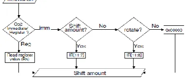
Generation of Shift Amount
Figure 6 explains how amount of shift is generated from instruction with use of flow chart.
Figure 6 : Flow chart to generate Shift amount
rn data, rm data, rs data, shift type, shift en, opcode, s, p, l, f out, immd out and inst no out are dec/exe pipeline
register outputs which are given to execution stage and br rst out and br add out are given to logic pc block.[10] In case of Branch instruction, pipeline is executed up to execution stage and instruction fetch is again started from the branch location. So, in case of branch instruction pipeline is stalled for 1-clock cycle.
Tab le 3.1 des crib es trut h tabl e for imp lem ent atio n of pip elin e regi ster s. Reg iste r con tain s St all Pau se Out put
0 0 0 inp
ut
0 0 1 outp
ut
0 1 0 0
0 1 1 0
1 0 0 0
1 0 1 0
1 1 0 0
1 1 1 0
Truth Table for Pipeline Register Logic
IV.INSTRUCTION SET
Implemented instruction in current version are listed in appendix. Decoding table and detailed explanation of this
instructions can be found in ARM instruction manual [1]. All instructions are executed conditionally depending on
COND field bits [31:28]. Instruction can be decoded from bits: bits [27:20] and bits [7:4].Instructions that implemented
can be classified in four categories. 1)Data Processing instructions: Instructions implemented allow three types of
operand operation. It is possible to use registers and a 12 bit immediate value. Here are the characteristics of its operands:[9]
destination (the result) : register (Rd)
operand 1: register (Rn)
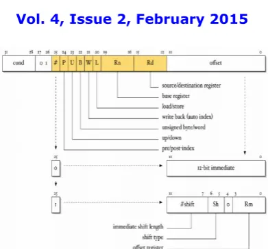
Copyright to IJAREEIE 10.15662/ijareeie.2015.0402150 805 Figure7 [1] explains format for data processing instruction. It also explains different interpretation in different bit conditions.
Decoding of bits is as follow:
Bits [27:26] = 00 is used to decode data transfer instruction.
S:
1 = update condition flag.
0 = Do not update condition flag.
Operand 2: Operand 2 is decoded on basis of value of bit 25.
Bit 25:
1 Immediate value
0 Register value
Immediate value: It is generated by rotating 8-bit immediate
value [7:0] to right by 4-bit rotating amount [11:8].
Register value: It is generated by further decoding operand 2
with bit 4.
Bit 4:
1 register shift
0 immediate shift
Register shift: operand 2 is generated by shifting bits of Rm [3:0] register by amount stored in Rs [11:8] register.
Immediate shift: operand 2 is generated by shifting bits of Rm [3:0] register by amount given in 5-bits [11:7].
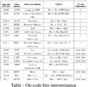
Bits [24:21]: These bits are used as Opcode in instruction. Decoding of opcode is explained in the bellow table [1].
There are three cases of selection of operands:
1. Instructions with three operands
2. Instructions with two operands without storing result (not Rd)
3. Instructions with two operands, a source and a destination (MOV,MVN)
Table : Op-code bits interpretation
2) Load/Store Instructions: Processor has load-store architecture and hence all data transfer is handled through load store instructions. This current version supports load and store instructions with register only. Word and Unsigned Byte data transfer: Instruction decoding is shown in Figure 8[1].
Decoding of bits is as follow:
Figure 8: Decoding of Load/Store Instruction
The P bit has two meanings
P == 0 indicates the use of post-indexed addressing. The base register value is used for the memory address,
and the offset is then applied to the base register value and written back to the base register.
P == 1 indicates the use of offset addressing or pre-indexed addressing (the W bit determines which). The
memory address is generated by applying the offset to the base register value.
The U bit indicates whether the offset is added to the base (U == 1) or is subtracted from the base (U == 0).
The B bit distinguishes between an unsigned byte (B == 1) and a word (B == 0) access. The W bit has two
meanings:
P == 0 If W == 0, the instruction is LDR, LDRB, STR or STRB and a normal memory access is
performed. If W == 1, the instruction is LDRBT, LDRT, STRBT or STRT and an unprivileged (User mode) memory access is performed.
P == 1 If W == 0, the base register is not updated (offset addressing).If W == 1, the calculated memory
address is written back to the base register (pre-indexed addressing).
3)Branch Instructions: Control of instruction execution is altered in two ways. One is load/move immediate value in PC and the other is using branch instruction and apply offset to jump. In data transfer instructions and load instructions by keeping destination Rd value as R15 (PC), PC can be loaded with new value. Branch instruction decoding is shown in Figure 9 [1].
Figure 9: Decoding of Branch Instruction
Decoding of bits is as follow:
Bits [27:25] = 101 is used to decode branch instruction.
Branch address: Address is calculated in following steps:
1. Sign-extending the 24 bit signed immediate to 30 bits
2. Shifting the result left two bits to form 32 bit value
3. Adding this to content of PC, this contains the address of the branch instruction plus 8 bytes.
In case of BL instruction address of the instruction next to branch is stored in LR (R14) register.
V. SIMULATION AND RESULTS
Copyright to IJAREEIE 10.15662/ijareeie.2015.0402150 807 multiplexer and an or-gate is used which are included in logic pc block, to take care of the branch instructions and to reset the fetch/decode pipeline registers. It loads instruction memory address in PC according to the multiplexer logic based on br addr input. If br addr is set to logic-00 then it loads the incremented PC and if br addr is set to logic-01 then it loads address generated by execution unit.
Simulated behaviour of Fetch Stage:
VI. CONCLUSION AND FUTURE WORK
The recent advances in portable applications and their continuous demand of high performance processor with low power consumption and small die size leads to development of efficient processor architecture such as ARM9. In this project architecture based on ARM9 has been designed with five stage pipeline which is capable of executing instructions in five clock cycles and a part of its instructions are implemented. Instruction decoding is kept same as standard ARM9 IP. Architecture is developed to support 5 stage pipeline, data forwarding and wait mechanism. All the instructions except branch and store, take 5 clock-cycles to execute. Branch instructions take 3 clock-cycle to execute provided that branch is taken. Memory store instructions takes 4 clock-cycles to store the date into memory (D-cache). Complete architecture and implemented instructions are verified using MODELSIM simulator with waveforms.
Improvements possible in current developed design are: IP can be modified to support more ARM9 instructions. IP can be modified to support more addressing modes (multiple data transfer, Half word data transfer). IP
can be modified to support interrupts and Thumb Instructions. IP can be modified to support media Instructions
REFERENCES
[1] ARM Architecture Reference Manual, issue 1ed.,ARM Limited, 110 Fulbourn Road Cambridge, England CB1 9NJ, July 2005.
[2] Prabhakar J., Senthilkumar M., Priya M.S., Mahalakshmi K., Sehgal P.K., Sukumaran V.G., "Evaluation of Antimicrobial Efficacy of Herbal Alternatives (Triphala and Green Tea Polyphenols), MTAD, and 5% Sodium Hypochlorite against Enterococcus faecalis Biofilm Formed on Tooth Substrate: An In Vitro Study", Journal of Endodontics, ISSN : 0099-2399, 36(1) (2010) pp. 83-86
[3] Wikipedia. (2010, July) ARM architecture. [Online].Available:http://en.wikipedia.org/wiki/ARM architecture.
[4] Ramkumar Prabhu, M., Reji, V., Sivabalan, A., "Improved radiation and bandwidth of triangular and star patch antenna", Research Journal of Applied Sciences, Engineering and Technology, ISSN : 2040-7459, 4(12) (2012) pp. 1740-1748.
[5] Intellectual property core, Altera cores [5] Free reference IP cores for FPGAs, http:/ / www. opencores. org/ faq. cgi/ section .[4]http://en.wikipedia.org/wiki/ARM architecture.
[6] Saravanan T., Saritha G., Udayakumar R., "A Robust H-infinity two degree of freedom control for electro magnetic suspension system", Middle - East Journal of Scientific Research, ISSN : 1990-9233, 18(12) (2013) pp. 1827-1831.
[7] StrongARM. (n.d.). Retrieved November15, 2010, from Wikipedia: http://en.wikipedia.org/wiki/Strong ARM. [8] Witek, R., & Montanaro, J. (1996). StrongARM-A high Performance Microprocessor. Compcon (pp. 1-5). IEEE.
[9] Saravanan, T., Saritha, G., "Buck converter with a variable number of predictive current distributing method", Indian Journal of Science and Technology, ISSN : 0974-6846, 6(S5) (2013) pp.4583-4588
[10] Intel StrongARM Processor, Companion Chip Optimized for Handheld Computing Devices. http://tinyurl.com/726zwjw.
[11] Saravanan, T., Srinivasan, V., Sandiya, V.P., "A two stage DC-DC converter with isolation for renewable energy applications", Indian Journal of Science and Technology, ISSN : 0974-6846, 6(S6) (2013) pp. 4824-4830.
[12] Palnitkar, S. (2006). A Guide to Digital Design and Synthesis (2nd ed). India: Dorling Kindersley Pvt. Ltd. [13]William J. Dally and JohnW. Poulton, Digital systems engineering. UK: Cambridge University Press, 1998.
[14] TVUK Kumar, B Karthik, EB Kumaran, Visual Secret Sharing Scheme for JPEG Compressed Images, Middle-East Journal of Scientific Research 12 (12), PP 1873-1880, 2012.
[16] Mr.B.Karthik, Dr.T.V.U. Kiran Kumar, N. Gomathi, Immobilizer Implementation using Mutual Authentication with enhanced security using 802.15.4 protocol,International Journal of Advanced Research in Electrical, Electronics and Instrumentation Engineering ,ISSN 2278 - 8875, pp 142-151, Vol. 1, Issue 3, September 2012.
[17] M.Jasmin,Bus Matrix Synthesis Based On Steiner Graphs For Power Efficient System On Chip Communications ,International Journal of Advanced Research in Electrical, Electronics and Instrumentation Engineering, ISSN 2278 - 8875 , pp 98-104,Vol. 1, Issue 2, August 2012. [18] M. Jasmin, A Low Power Pipelined FFT/IFFT Processor for OFDM Applications,International Journal of Advanced Research in Electrical, Electronics and Instrumentation Engineering,ISSN (Print) : 2320 – 3765, pp 4712-4721, Vol. 2, Issue 10, October 2013.
[19] M Jasmin, Low Power Design of the Processer Based on Architecture Modifications,International Journal of Advanced Research in Electrical, Electronics and Instrumentation Engineering,ISSN: 2278 – 8875, pp 2922-2927, Vol. 2, Issue 7, July 2013.