Scholarship at UWindsor
Scholarship at UWindsor
Electronic Theses and Dissertations Theses, Dissertations, and Major Papers
2011
A Prototype CVNS Distributed Neural Network
A Prototype CVNS Distributed Neural Network
Golnar Khodabandehloo University of Windsor
Follow this and additional works at: https://scholar.uwindsor.ca/etd
Recommended Citation Recommended Citation
Khodabandehloo, Golnar, "A Prototype CVNS Distributed Neural Network" (2011). Electronic Theses and Dissertations. 433.
https://scholar.uwindsor.ca/etd/433
by
Golnar Khodabandehloo
A Dissertation
Submitted to the Faculty of Graduate Studies through
the Department of Electrical and Computer Engineering in Partial Fulfillment
of the Requirements for the Degree of Doctor of Philosophy at the
University of Windsor
All Rights Reserved. No Part of this document may be reproduced, stored or otherwise
retained in a retreival system or transmitted in any form, on any medium by any means
by
Golnar Khodabandehloo
APPROVED BY:
Y. Savaria
Department of Electrical Engineering, Polytechnique Montral
A. Jaekel
School of Computer Science, University of Windsor
C. Chen
Department of Electrical and Computer Engineering, University of Windsor
M. Khalid
Department of Electrical and Computer Engineering, University of Windsor
M. Ahmadi
Department of Electrical and Computer Engineering, University of Windsor
M. Mirhassani
Department of Electrical and Computer Engineering, University of Windsor
G. Reader
Department of Mechanical, Automotive and Materials Engineering, University of Windsor
Declaration of Previous Publication
This thesis includes 5 original papers that have been previously published/submitted for
publication in peer reviewed journals, as follows:
Thesis Chapter Publication title Publication status
Chapters 3,4, and 6 A prototype CVNS distributed neural network using synapse-neuron modules Submitted
Chapter 5 A 16-level current-mode CVNS memory Published Chapter 5 CVNS-based storage and refreshing scheme for a multi-valued dynamic memory In-press
Chapter 2 Resistive-type CVNS distributed neural networks with improved noise to signal ratio Published Chapter 4 Analog implementation of a novel resistive-type sigmoidal neuron In-press
I certify that I have obtained a written permission from the copyright owner(s) to include
the above published material(s) in my thesis. I certify that the above material describes
work completed during my registration as graduate student at the University of Windsor.
I declare that, to the best of my knowledge, my thesis does not infringe upon anyone’s
copyright nor violate any proprietary rights and that any ideas, techniques, quotations, or
any other material from the work of other people included in my thesis, published or
oth-erwise, are fully acknowledged in accordance with the standard referencing practices.
Fur-thermore, to the extent that I have included copyrighted material that surpasses the bounds
of fair dealing within the meaning of the Canada Copyright Act, I certify that I have
thesis. I declare that this is a true copy of my thesis, including any final revisions, as
ap-proved by my thesis committee and the Graduate Studies office, and that this thesis has not
Abstract
Artificial neural networks are widely used in many applications such as signal processing,
classification, and control. However, their practical implementation is challenging due to
the number of inputs, the cost of storing the required weights, and the difficulty in realizing
the activation function.
In this work, Continuous Valued Number System (CVNS) distributed neural networks
are proposed which are providing the network with self-scaling property. This property aids
the network to cope spontaneously with different number of inputs. The proposed CVNS
DNN can change the dynamic range of the activation function spontaneously according to
the number of inputs providing a proper functionality for the network.
In addition, multi-valued CVNS DRAMs are proposed to store the weights as CVNS
digits. These memories scan store up to 16 level, equal to 4 bits, on each storage cell.
In addition, they use error correction codes to detect and correct the error over the stored
values.
A synapse-neuron module is proposed to decrease the design cost. It contains both
synapse and neuron and the relevant components. In these modules, the activation function
is realized through analog circuits which are far more compact compared to the digital
Furthermore, the redundancy between CVNS digits, together with the distributed
struc-ture of the neuron make the proposal stable against process variations and reduce the noise
To my family,
There are several people who deserve my sincere thanks for their generous contributions
to this project. I would first like to express my sincere gratitude and appreciation to Dr.
Mitra Mirhassani and Dr. Majid Ahmadi, my supervisors for their invaluable guidance and
constant support throughout the course of this thesis work.
In addition to my advisors, I would like to thank the rest of my thesis committee: Dr.
Chunhong Chen and Dr. Mohammed Khalid from the electrical and computer engineering
department, Dr. Arunita Jaekel from the school of computer science, and Dr. Yvon Savaria
from the Polytechnique Montreal for their participation in my seminars, reviewing my
thesis, and their constructive comments.
Also, I would like to thank Dr. Roberto Muscedere for his assistants regarding the VLSI
CAD tools and facilities used during the course of the project.
I am grateful to my colleague, friend, and partner Ashkan H. Namin who has supported
and believed in me.
Finally, my deepest gratitude goes to my family for their unconditional love, support,
Contents
Declaration of Previous Publication iv
Abstract vi
Dedication viii
Acknowledgments ix
List of Figures xiii
List of Tables xvi
List of Abbreviations xvii
1 Introduction 1
1.1 Summary of Contributions . . . 7
1.2 Outline of the Thesis . . . 7
2 CVNS Distributed Neural Network 9 2.1 Previous Structures of Resistive-Type ANNs . . . 9
2.1.1 Lumped Neural Network . . . 10
2.1.2 Conventional Distributed Neural Network . . . 11
2.2.1 Scalability . . . 16
2.2.2 2-2-1 XOR . . . 16
2.3 CVNS Fully Distributed Neural network . . . 17
2.4 Stochastic Model . . . 18
2.5 Comparison . . . 23
2.6 Conclusion . . . 24
3 Truncated CVNS Distributed Neural Network 26 3.1 Truncated CVNS DNN . . . 27
3.2 Effect of Truncation on Performance . . . 31
3.3 NSR Calculation . . . 33
3.4 Conclusion . . . 35
4 Synapse-Neuron Module 37 4.1 CVNS DRAM . . . 38
4.2 Multiplier Module . . . 41
4.3 Interface Circuit . . . 42
4.4 Sigmoidal Neuron . . . 44
4.5 Voltage-Mode ADC . . . 45
4.6 Conclusion . . . 47
5 CVNS Multi-Valued Dynamic Memory 48 5.1 CVNS Modifications for Implementation . . . 51
5.2 Noise Margin and Error Correction Based on CVNS . . . 54
5.3 CVNS-Based Storage Circuitry . . . 58
5.4 CVNS-Based Refreshing Scheme and Circuits . . . 64
5.4.1 Analog to Digital Converter . . . 66
5.4.1.1 Current Comparators . . . 70
5.4.2 Digital to Analog Converter . . . 72
5.5 Simulation Results and Comparisons . . . 77
5.6 Conclusion . . . 81
6 A 4-3-2 CVNS DNN using Synapse-Neuron Modules 83
6.1 Prototype CVNS DNN . . . 83
6.2 Comparisons . . . 87
6.3 Conclusion . . . 89
7 Conclusions and Future Work 90
7.1 Conclusions . . . 90
7.2 Future Work . . . 91
References 93
1.1 Block diagram of the CVNS digit generation from binary digits. . . 4
2.1 (k+ 1)-input resistive-type lumped neural network. . . 10
2.2 Block diagram of a(k+ 1)-input resistive-type DNN. . . 11
2.3 Proposed resistive-type CVNS DNN configuration. . . 13
2.4 Block diagram representation of the CVNS multiplication (equation (2.5)). . 14
2.5 Scalability of the proposed DNN for a sigmoidal activation function. . . 17
2.6 Block diagram of the2−2−1XOR network. . . 18
2.7 Off-line network training by back propagation algorithm. . . 19
2.8 (k+ 1)-input resistive-type CVNS fully distributed neural network. . . 20
2.9 Comparison for input range of [9,25]: (a) Stochastic Gain Function for Adaline, NSR for (b) Adaline, (c)5-layer Madaline, (d)10-layer Madaline. 23 3.1 Final multiplication result in a high resolution environment. . . 30
3.2 Final multiplication result in a low resolution environment. . . 31
3.3 Simulation result of an XOR based on the truncated CVNS DNN. . . 31
3.4 NSR comparisons for Adalines and5-layer Madalines. . . 35
4.1 Block diagram of the proposed synapse-neuron module. . . 38
4.2 Block diagram of the13-bit multi-valued DRAM. . . 39
4.4 Block diagram of the multiplier module. . . 41
4.5 Block diagram of the partial multiplication module. . . 41
4.6 Simulation result of ‘1,1111,1010,1011’ multiplied by ‘0111’. . . 42
4.7 Layout of the multiplication module. . . 43
4.8 Schematic of the interface circuit. . . 43
4.9 Schematic of the proposed resistive-type neuron to realize the sigmoid function. . . 44
4.10 Simulation result of the sigmoidal neuron. . . 45
4.11 schematic of a set of inverters used in the proposed voltage-mode ADC. . . 46
5.1 Block diagram of simplified CVNS digit generation using the group method. Squares show the weighted sum operation units. . . 52
5.2 Block diagram of the modified CVNS digit generation withψ = 4andν= 1. 55 5.3 Overall block diagram of the proposed memory . . . 59
5.4 General storage scheme for a16-bit input. In order to increase the reliabil-ity of the cells, the LSB input to each cell is repeated and is used for error correction. . . 59
5.5 Self-biased dynamic current mirror memory (current copier) . . . 60
5.6 Simulation results of different resistors in storage cell. . . 62
5.7 Storage cell layout . . . 63
5.8 Simulation result of storage cell layout for011110binary input. . . 63
5.9 Block diagram of the refreshing system for a CVNS DRAM cell. . . 65
5.10 Block diagram of the ADC . . . 66
5.11 4-bit ADC layout . . . 69
5.12 Schematic of a current comparator . . . 71
5.13 Schematic of a current source . . . 71
5.14 Schematic of the first current mirror . . . 73
5.16 Overall configuration of the4-bit DAC. . . 74
5.17 Schematic of a one-bit weighted current mirror . . . 75
5.18 DAC layout . . . 76
5.19 DAC layout simulation results for input of011110 . . . 77
5.20 Post layout simulation result of total circuit for011100 binary input. . . 78
5.21 Block diagram of the DRAM proposed by Lee et al. [1] . . . 80
6.1 Block diagram of the4-3-2CVNS DNN. . . 84
6.2 Training pattern set for the4-3-2CVNS DNN. . . 85
6.3 Layout of the proposed4-3-2CVNS DNN. . . 86
List of Tables
1.1 An example for radix-10CVNS digits . . . 4
2.1 NSR of sigmoidal Adalines fromcase study 2 . . . 21
2.2 Comparison of different sigmoidal Adalines for ak+ 1input . . . 24
3.1 Multiplication partial results forcase study 1. . . 30
5.1 An example for the CVNS digits with different group lengths and digit links 54 5.2 An example for error correction when the binary input is1011,0101,1110,0011 58 5.3 Schematic storage cell and layout storage cell simulation results . . . 64
5.4 Values of all currents in the ADC block diagram . . . 67
5.5 Extraction ofx3andx2from the output of current comparators. . . 67
5.6 Comparison made between the proposed ADCM and some published meth-ods for a4-bit ADC . . . 68
5.7 Schematic ADC and layout ADC simulation results . . . 70
5.8 Transistor sizes for each current source in the layout . . . 72
5.9 Transistor sizes for each current mirror . . . 76
5.10 Schematic DAC and layout DAC simulation results . . . 77
Adaline Adaptive Linear Neuron. ADC Analog to Digital Converter. ANN Artificial Neural Network.
CMOS Complementary Metal-Oxide-Semiconductor.
CN Common Node.
CVNS Continuous Valued Number System. DAC Digital to Analog Converter.
DNN Distributed Neural Network.
DRAM Dynamic Random Access Memory.
ECC Error Correction Code.
FDNN Fully Distributed Neural Network.
IEEE Institute of Electrical and Electronics Engineers. LID Least Informed Digit.
LSB Least Significant Bit.
LUT Look-Up-Table.
Madaline Multiple Adaline.
MID Most Informed Digit.
MSB Most Significant Bit. NSR Noise to Signal Ratio. QLG Quantized Level Generator.
SCCV Simulated Constant Current Value.
TSMC Taiwan Semiconductor Manufacturing Company.
Chapter 1
Introduction
In the past decades, studies have been performed to use Artificial Neural Networks (ANNs)
in different applications such as signal processing, pattern recognition, control, and many
others [2–8]. One of the important features of an ANN is its scalability which means how
the network responds if the number of inputs changes as different applications may need
different number of inputs.
In conventional lumped ANNs, there is one neuron corresponding to all the synapses in
each layer, where changing the number of inputs results in malfunctioning of the network
[9]. In the case of a sigmoidal neuron, increasing the number of inputs would cause a larger
saturation area for the neuron which changes the sigmoidal function to a hard limiting
function. Decreasing the number of inputs, on the other hand, will result in a low-gain
function. To overcome these problems, the neuron should be redesigned whenever the
number of inputs changes which is not possible in hardware implementations. Therefore,
the application of a lumped ANN becomes limited to applications with a certain number of
Resistive-type Distributed Neural Network (DNN) was introduced as an alternative for
lumped neural networks [2, 3, 9, 10]. DNNs provide a self-scaling property for the network
to cope with variable number of inputs, spontaneously. In DNNs, there are sub-neurons
instead of neurons. Each sub-neuron is dedicated to one input; consequently, changing
the number of inputs changes the number of sub-neurons. Therefore, DNNs can stretch or
shorten the dynamic range of the activation function to keep the overall neuron
characteris-tic in its proper functionality for different number of inputs. This causes an instant change
in the dynamic range of the overall activation function according to the number of inputs.
The use of sub-neurons in DNNs also provides some advantages for the network such as
higher immunity to noise and process variations [9]. Noise to Signal Ratio (NSR) can be
used to study the noise immunity of the ANNs [11]. Generally, a distributed configuration
decreases the NSR compared to the lumped networks [3, 9, 10]. Here, NSR is used instead
of signal to noise ratio to create a simple analytical expression.
In this work, a structure for feed-forward neural networks is proposed based on the
Continuous Valued Number System (CVNS) as a derivative of conventional DNNs. The
CVNS [12, 13] is a redundant number system which has been successfully employed in
building high performance low power arithmetic units, multi-valued memories, and neural
networks [14–20].
Considering inputs and outputs of the CVNS memory as binary digits, it is shown that
there is an easy way for converting digits from binary to the CVNS and vise versa. The
general representation of an (m+ 1)-bit binary value is as follows.
x=±
m
X
i=0
xi·βi (1.1)
wherexi represents binary digits andβshows the radix;β = 2for a binary radix.
For example, a binary value ofx= 101001is equal to1×25+ 0×24+ 1×23+ 0×
22+ 0×21+ 1×20 = 41.
A CVNS set is an ensemble of multiple CVNS digits, ((x))i, which are generally
calledcascade Digit Generation, starts from the first CVNS digit and generates digits one
by one in series; each digit is extracted from the previously generated digits.
An other method called Modular Reduction Digit Generation is used in this work. It
generates all the CVNS digits at the same time, in parallel, and independent to each other.
Thus, this method provides a higher speed of conversion together with a lower complexity
compared to the series method and is as follows.
((x))n−i =
³ x
M ·β
n−i+1´modβ =³ x
M ·2
n−i+1´mod2 (1.2)
where n is the maximum index of the CVNS digits, 0 ≤ i ≤ n. M is the maximum
representation range, and β is the CVNS radix which is chosen low, equal to2 (β = 2),
in order to reduce the complexity of the circuit further more. modstands for the modular
reduction operation on any continuous real value such that(a)modβ = a−I×β where
0≤(a)modβ < β. I is an integer (I = 0,1,· · · , β−1) which in this case is either0or1.
In order to simplify the conversion between binary and CVNS, the maximum range of
the representation for both the binary and the CVNS systems is selected as2m+1 = 2n+1 =
M. Therefore, the number of binary digits, m+ 1, and the CVNS digits,n + 1, are the
same.
Under these conditions, a CVNS digit is directly generated from its corresponding
bi-nary digits through a general expression by modifying expression (1.2) as follows.
((x))n−j = mX−j
i=0
xi·2i+j−m, j = 0,1, ..., n (1.3)
By eliminatingmod2operation in digit generation, this pre-congruent relation reduces
the number of required gates for system implementation. According to the expression given
by the equation (1.3), the CVNS digit generation directly from the binary digits can be
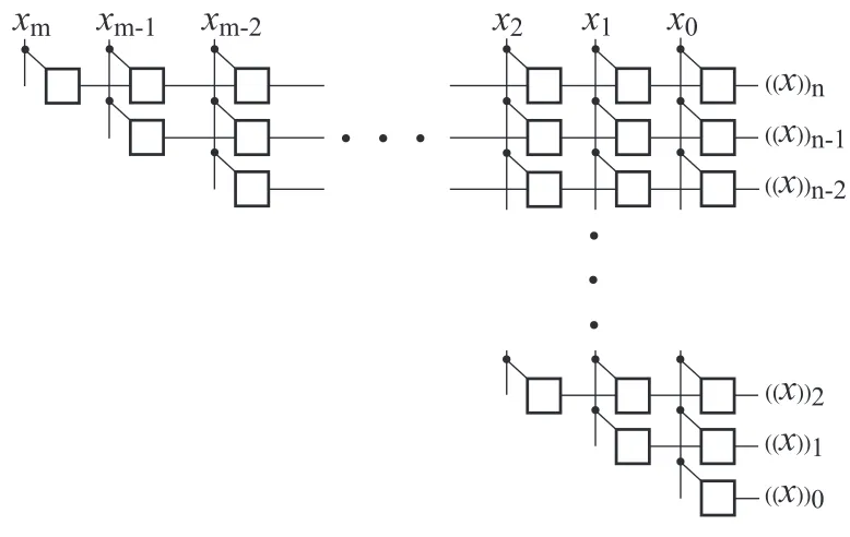
realized employing simple weighted current mode mirrors. A block diagram representation
of equation (1.3) is shown in Figure 1.1, where squares show the weighted sum operation
x
mx
m-1x
m-2x
2x
1x
0((
x
))n ((x
))n-1((
x
))2 ((x
))1 ((x
))0 ((x
))n-2.
. . .
.
.
.
.
.
.
.
.
.
. .
.
.
. .
. .
.
.
. .
. .
Figure 1.1: Block diagram of the CVNS digit generation from binary digits.
Table 1.1 shows the first five CVNS digits,((x))i, of an arbitrary chosen value in
radix-10with maximum level of redundancy. Here, the original value is89.0537412.
Table 1.1: An example for radix-10CVNS digits
((x))n ((x))n−1 ((x))n−2 ((x))n−3 ((x))n−4
8.90537412 9.0537412 0.537412 5.37412 3.7412
In Table 1.1,{8}appears only in the first CVNS digit,{9}is repeated in only first two
CVNS digits while{3,7,4,1,2}are repeated in first five CVNS digits. In other words, in
a CVNS digit set, lower index CVNS digits can be rebuilt from higher index CVNS digits
(((x))n−3 = (((x))n−2 × 10)mod10 = (((x))n−1 ×10²)mod10 = (((x))n× 103)mod10).
Also, lower index CVNS digits can help in recovering the higher index ones (((x))n =
The CVNS representation also offers some degrees of freedom in selecting some
rep-resentation dimensions such as the level of information overlap between the digits and the
number of the required CVNS digits according to design demands. The CVNS digit
gen-eration is limited by the resolution of the environment. Therefore, truncation methods are
applied to the CVNS digits to make them cope with lower resolution environments while
still keeping the CVNS properties [14, 15]. One of the advantages of applying these
meth-ods is reducing the area consumption; however, it may result in lower accuracy as well.
Consequently, the CVNS digits have information overlap with each other; every digit
has some level of knowledge about the digits with lower indices in the same set. This digit
level redundancy is used to detect and correct errors in the digit set which makes the system
more robust against the noise. The proposed CVNS DNN has all the advantages of using
DNNs; furthermore, it results in a reduced NSR for the network compared to conventional
DNNs. This makes the CVNS DNNS a great candidate for hardware implementations.
The CVNS can be implemented through current-mode analog circuitries which
gener-ally provide lower noise, lower voltage swing, and the ability of working with lower power
supply voltages [21–23]. Nevertheless, some functions such as addition can be easily
real-ized through current-mode circuitries.
In this work, a current-mode synapse-neuron module is designed based on the CVNS
which can be used as the building block for a wide variety of applications. The
synapse-neuron module decreases the design cost and increases the fan-out [3]. The weights to this
module are considered to be equal to13bits. Truncated CVNS digits equivalent to weights
are generated and stored in multi-valued DRAMs with the ability of error correction [14,
15]. These memories can store up to16-level equivalent to4-bit on each storage cell.
Each two adjacent CVNS digits, in the proposed DRAM, has equivalent to one binary
digit overlap; this common digit is used for error correction in the system. This
configura-tion provides a novel multi-valued DRAM with increased noise margin and reduced area.
ADC has a parallel configuration and can convert two bits simultaneously. It can reduce
the overall delay of the refreshing circuitry.
The proposed DRAM has to be refreshed continuously; the voltage over the storing
capacitor drops after a while due to the leakage currents of the storage cell. During the
refreshing cycle, the storage capacitor is charged to the correct value indicated by the error
correction codes.
Except for the multi-valued memory, the proposed synapse-neuron module contains
multiplication module, interface module, and sub-neuron. The multiplication module
mul-tiplies the truncated CVNS digits by the input. A voltage-mode Analog to Digital Converter
(ADC) extracts the digits of the input for the sake of multiplication. The inputs are
con-verted to a4-bit value and are applied as multipliers to the multiplication modules.
Sign, the 13th bit of the weight, is applied to the multiplier output in the interface
module releasing the final synapse output which goes to a Common Node (CN). CN is
common between all the synapse-neuron modules in a layer and acts as an input/output
node. In this node, currents from synapses are added up together and divided by the number
of neurons. Accordingly, all the neurons receive an identical current. Each
sub-neuron in the synapse-sub-neuron module decides the output value based on this current.
The sigmoid function is selected as the activation function which always has a value
be-tween0and1. A new analog resistive-type neuron is designed which generates the sigmoid
function based on the transistor characteristics in both triode and saturation regions.
To justify the design concept, the proposed synapse-neuron modules are used to
de-sign a prototype4-3-2network with four digital inputs and two final digital outputs. This
prototype is trained off-line based on a classification pattern. The circuitries are designed,
simulated, and laid out in 0.18µm TSMC CMOS technology [25] using a power supply
1.1 Summary of Contributions
In this dissertation, a new family of the CVNS DNNs are introduced. The scalability and
noise immunity of the proposal are studied and compared to the lumped and conventional
distributed networks. Studies show that it outperforms the previous structures because of
its low NSR.
The proposed CVNS DNN is implemented considering the environmental resolution
limitations which is equal to4-bit in the employed technology. Multi-valued DRAMs with
error correction abilities are designed to convert and store the weights in the form of the
CVNS digits. The proposed multi-valued memories are a significant progress in this field
because of their lower area and power consumption as well as lower refreshing cycle time.
A 4-3-2 network is designed, laid out, and trained off-line based on a pattern set. The
post-layout simulations are performed which show the proper functionality of the design.
1.2 Outline of the Thesis
The next chapters are organized as follows. In Chapter 2, the structures of a typical lumped
ANN and a conventional DNN are shown and the proposed CVNS DNN structure is
in-troduced. It also studies the scalability in the proposed DNN, and shows how the CVNS
DNN is used to solve an XOR problem. Designing CVNS fully distributed neural network
according to the CVNS DNN is discussed. A Stochastic NSR model is used, and NSR of
different sigmoidal Adalines are compared together.
Chapter 3 presents the environmental limitations for implementation of the proposed
CVNS DNN. Truncated methods are used to cope with these limitations. The effect of
truncation on the performance and noise immunity are studied. Simulations show that
the truncated CVNS DNN still has lower NSR compared to the lumped and conventional
distributed neural networks.
synapse-neuron module are the storage module, multiplication module, interface module, and
sub-neuron. For each sub-module, the task and circuitries are discussed. The synapse-neuron
module is designed in current-mode. There is also a voltage-mode ADC to convert the
output of each layer to4bits that can be used as the input to the next layer.
The proposed current-mode multi-valued CVNS DRAM is introduced in detail in
Chap-ter 5. In this chapChap-ter, the CVNS is described and the truncated CVNS is introduced in
detail. Sub-modules of the CVNS DRAM and their circuitries are presented. The
pro-posed DRAM is using a series combination of ADC and DACs for conversion, storage, and
correction. A fast current-mode ADC method is proposed and compared to current-mode
ADC methods in literature. A method for decreasing the refresh rate is also proposed. Error
correction in this DRAM is discussed based on the CVNS features. Finally, the proposed
memory is compared to current-mode memories in literature.
In chapter 6, a prototype 4-3-2 network is designed. This network is trained based
on a pattern set to solve a classification problem. The weights and biases are calculated in
MATLAB and used for post-layout simulations. The final layout and post-layout simulation
results are also shown in this chapter. The circuitries are designed in0.18µmTSMC CMOS
technology.
Chapter 2
CVNS Distributed Neural Network
In this chapter, a new family of resistive-type feed-forward distributed neural networks is
proposed based on the CVNS. The proposed CVNS DNN is used for off-line training of a
prototype XOR. A stochastic model is employed to formulate NSR of a sigmoidal Adaline
based on the proposed CVNS DNN. This is compared to the NSR of sigmoidal Adalines
based on other comparable structures. A fully distributed neural network is designed based
on the proposed CVNS DNN which can provide even lower level of NSR in the network
while using more neurons. The reduced sensitivity to noise property of the proposed
struc-tures makes them robust against process variations; hence, they are potential candidates for
hardware applications such as industrial sensors.
2.1 Previous Structures of Resistive-Type ANNs
In resistive-type ANNs, the neuron function is realized by a nonlinear load that receives
same node [3, 9, 10].
Although numerous designs of neural networks have been reported, in this chapter, the
basic structure of resistive-type feed-forward neural networks is categorized into two main
groups: lumped and distributed neural networks.
2.1.1 Lumped Neural Network
Lumped ANN is the original structure of neural networks in which all synapses are
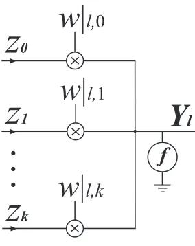
con-nected to one neuron in each layer. The block diagram of a (k + 1)-input resistive-type
lumped ANN for thelthlayer is shown in Figure 2.1. Each input is multiplied by a
synap-tic weight. All of the multiplication results are added up together in a common node, and
the result goes to an activation function to generate the final output.
z
0►
.
.
.
.
z
1►
z
k►
Y
lw
|
l,
0
w
|
l,
1
w
|
l,k
f
Figure 2.1:(k+ 1)-input resistive-type lumped neural network.
The output of the neuron,Yl, is generated through the following equation.
Yl=f(
k
X
t=0
Zt×w|l, t) (2.1)
whereZtshows thetthinput, and w|l, tshows its corresponding synaptic weight.
2.1.2 Conventional Distributed Neural Network
Resistive-type DNNs provide one neuron for each synapse. The block diagram of a(k+1)
-input resistive-type DNN [3, 9, 10] is shown in Figure 2.2.
Here, instead of one neuron, sub-neurons are used to realize the activation function.
The input and weight multiplication results are added up together. The result is divided by
the number of sub-neurons so that each sub-neuron receives the same amount of current.
It should be noted that in each layer, all the sub-neurons have the same activation function.
The output of such a network is calculated as follows.
Yl =f(
1
k+ 1
k
X
t=0
Zt×w|l, t) (2.2)
►
.
.
.
.
►
►
.
.
f
f
f
.
w
|
l,
0
w
|
l,
1
w
|
l,k
Y
lz
0z
1z
kFigure 2.2: Block diagram of a(k+ 1)-input resistive-type DNN.
As there is one sub-neuron corresponding to each input, the number of sub-neurons
changes by the number of inputs. This self-scaling property of the DNN causes an increase
or a decrease in the dynamic input range of the activation function as the number of inputs
increases or decreases, respectively. The scalability feature of DNNs is used to build a new
2.2 CVNS Distributed Neural Network
The proposed network is a distributed neural network in which weights are stored as CVNS
digits. A family of CVNS neural networks was introduced in [20] where the output was
generated from a Reverse Evolution (RE) unit using complicated sub-functions. In the
proposed network, the design is modified to avoid RE and sub-functions which decreases
the network complexity and makes it more suitable for practical hardware implementations.
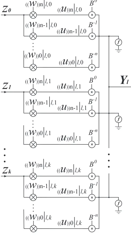
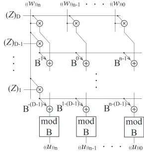
Figure 2.3 shows the proposed (k+ 1)-input resistive-type CVNS DNN configuration
for thelth layer.
In Figure 2.3, ((w))n−j|l,t (j = 0,1, ..., n and t = 0,1, ..., k) stands for the CVNS presentation of weights which are generated through the following equation.
((w))n−j|l,t = (
wt
M ∗B
j+1)mod B j = 0,1, ..., n (2.3)
wherewtstands for the value of the weight corresponding to thetth input,M is the
maxi-mum acceptable value of weights, andB is the CVNS radix.
In a CVNS digit set, digits with higher indices have information overlap with the lower
index digits. For example the equivalent CVNS digits of the randomly chosen value of
wt = 31.89for M = 100 andB = 10are ((w))3 = 3.189, ((w))2 = 1.89, ((w))1 = 8.9,
((w))0 = 9. These CVNS digits can be shown in a CVNS digit set as{3.189,1.89,8.9,9}.
The CVNS multiplication [13] of Zt (t = 0,1, ..., k) and ((w))n−j (j = 0,1, ..., n) is
calculated as follows.
First, the digits of the multiplier, (Z)D−d, are extracted as is shown in the following
equation.
(Z)D−d = (Zt×Bd)mod B−
(Zt×Bd+1)mod B
B (2.4)
whereDshows the number of digits ofZtandd= 0,1, ..., D−1.
►
. . .
((
w
))n|
l,0. . ► . . . . . ► . . . . .
.
.
.
.((
u
))n|
l,0 B0 B-1 . . ..
.
.
f f fz
0z
1z
kY
l B-n B0 B0 B-1 B-1 B-n B-n ((w
))n-1|
l,0((
u
))n-1|
l,0((
u
))0|
l,0 ((w
))0|
l,0((
w
))n|
l,1((
u
))n|
l,1((
w
))n|
l,k((
u
))n|
l,k ((w
))n-1|
l,1((
u
))n-1|
l,1((
w
))n-1|
l,k((
u
))n-1|
l,k ((w
))0|
l,1((
u
))0|
l,1((
w
))0|
l,k((
u
))0|
l,kFigure 2.3: Proposed resistive-type CVNS DNN configuration.
following equation. The block diagram representation is shown in Figure 2.4.
((u))n−j = Z
O
((w))n−j
= {(Z)D ×((w))n−j
+ D−1
X
i=1
(Z)D−i ×((w))n×Bj−i}mod B (2.5)
(
Z
)
D((
w
))n ((w
))n-1 ((w
))0.
.
((
u
))n.
.
.
.
.
.
.
.
.
.
.
.
. . .
.
.
.
. . .
B
-1mod
B
((
u
))n-1 ((u
))0(
Z
)
D-1(
Z
)
1B
0B
n-1B
-(D-1)B
1-(D-1)B
n-(D-1).
.
.
mod
B
mod
B
Figure 2.4: Block diagram representation of the CVNS multiplication (equation (2.5)).
multiplier ofZt= 2.14(digits are[2,1,4]) and a CVNS digit set multiplicand of{3.189,1.89,8.9,9}
withB = 10is as follows:
((u))3 = {2×3.189 + 1×3.189×10−1+ 4×3.189×10−2}mod10 = 6.82446
((u))2 = {2×1.89 + 1×3.189×100+ 4×3.189×10−1}mod10 = 8.2446
((u))1 = {2×8.9 + 1×3.189×101+ 4×3.189×100}mod10 = 2.446
((u))0 = {2×9.0 + 1×3.189×102+ 4×3.189×101}mod10 = 4.46
Digits in the multiplication output set,{6.82446,8.2446,2.446,4.46}, are CVNS digits
digit set.
(((x))n−j ×B)mod B = ((x))n−j−1 j = 0,1, ..., n (2.6)
As it is shown in equation (2.6), there is a redundancy between the CVNS digits. Lower
index CVNS digits can be calculated from the higher index digits; however, the process can
not be reversed. In other words, the higher the index of a CVNS digit is, the higher the level
of its information will be. However, to add the CVNS digits together, they have to be of
the same information level. To meet this requirement, ((u))n−j|l,t is multiplied by B−j
(j = 0,1, ..., n) in Figure 2.3.
In Figure 2.3, the total output of the CVNS DNN is calculated asYl =f(y)whereyis
generated from the CVNS multiplication outputs as follows.
y = 1
k+ 1{((u))n|l,0+
((u))n−1|l,0
B +...+
((u))0|l,0
Bn
+((u))n|l,1+
((u))n−1|l,1
B +...+
((u))0|l,1
Bn +...
+((u))n|l,k+
((u))n−1|l,k
B +...+
((u))0|l,k
Bn } (2.7)
From the CVNS features, it can be observed that CVNS addition of different CVNS
digit sets results in CVNS digits as well. The following example shows the CVNS addition
of four randomly chosen CVNS digit sets: {2.345, 3.45, 4.5, 5}, {7.891, 8.91, 9.1, 1},
{3.042, 0.42, 4.2, 2}, and{9.157, 1.57, 5.7, 7}.
(2.345 + 7.891 + 3.042 + 9.157)mod10 = 2.435
(3.45 + 8.91 + 0.42 + 1.57)mod10 = 4.35
(4.5 + 9.1 + 4.2 + 5.7)mod10 = 3.5
(5 + 1 + 2 + 7)mod10 = 5
The output digit set is a CVNS digit set according to equation (2.6).
In equation (2.7), the CVNS digits with the same index can be added up together as
follows.
It should be noted thatA=A mod B+I ×B whereI shows the quotient ofAdivided byB. Therefore, equation (2.8) can be rewritten as the following equation.
((u))n−j|l,0+ ((u))n−j|l,1+...+ ((u))n−j|l,k = ((y))n−j|l+In−j×B (2.9)
According to equation (2.9), equation (2.7) can be represented as follows.
y= 1
k+ 1{((y))n|l+
((y))n−1|l
B +...+
((y))0|l
Bn +Cons} (2.10)
whereConsis equal to n
X
j=0
In−j×B
Bj .
2.2.1 Scalability
For studying the self-scaling property of the proposed DNN, the value of the total current
entering the sub-neurons,y×(k+ 1), is considered to be between−60µAand60µAfor
1-input (k = 0). Consequently for 5-input (k = 4), the corresponding current, y×(5),
will be in the range of−300µAand300µA. Self-scaling property of the proposed DNN is
shown in Figure 2.5 where it compares the output for networks with1and5inputs together
for a sigmoidal activation function.
As is shown in Figure 2.5, the network is properly stretching the dynamic range to cope
with the increased number of inputs. Note that without a proper scaling, the output of5
-input case will be equal to0V for all inputs in the range of[−300µA,−60µA]and will be
1.8V for inputs in the range of[60µA,300µA].
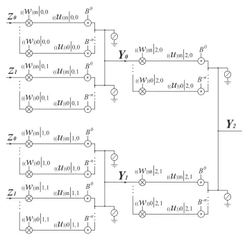
2.2.2 2-2-1 XOR
The proposed CVNS DNN is used to build a prototype2−2−1XOR as is shown in Figure
2.6.
Here, B is chosen equal to10, sigmoid function is chosen as the activation function,
and n is selected equal to 5. The network is trained off-line using the back propagation
−3000 −250 −200 −150 −100 −50 0 50 100 150 200 250 300300 0.2
0.4 0.6 0.8 1 1.2 1.4 1.6 1.8
Input Current (
µ
A)
Out
p
ut Voltage
(V)
1 Input 5 Input
Figure 2.5: Scalability of the proposed DNN for a sigmoidal activation function.
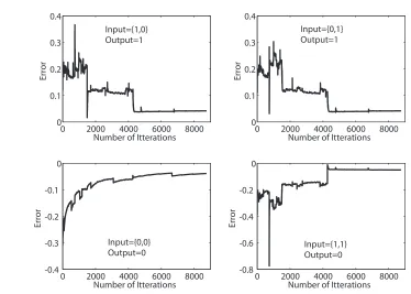
The training result is shown in Figure 2.7. Random sets of weights are selected for
initialization. The error from the ideal value is less than0.05(5.0%) for all input
combina-tions.
2.3 CVNS Fully Distributed Neural network
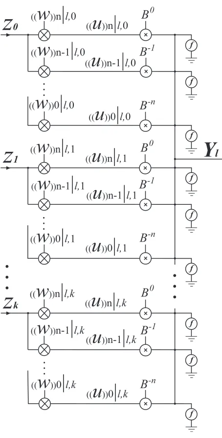
Based on the proposed CVNS DNN, a Fully Distributed Neural Network (FDNN) is
intro-duced. In this fully distributed CVNS network, the number of neurons depends not only
on the number of inputs,k+ 1, but also on the number of the CVNS digits in each CVNS
digit set of weights,n+ 1.
The block diagram of the proposed CVNS FDNN with(k+ 1)-input is shown in Figure
2.8.
The output isYl=f(y), whereyis calculated using the following equation.
y= 1
(k+ 1)(n+ 1){((y))n|l+
((y))n−1|l
B +...+
((y))0|l
► . . . ► . . . . . . . . . . . . . . ► . . . ► . . . . . . . . . . . . . . ► . . . ► . . . . . . . . . . . . . .
Y
0Y
1Y
2 B0 B0 B0 B0 B0 B0 B-n B-n B-n B-n B-n B-nz
0z
0z
1z
1((
w
))n|
0,0((
u
))n|
0,0((
w
))0|
2,1((
u
))0|
2,1((
w
))0|
0,0((
u
))0|
0,0((
w
))n|
0,1((
u
))n|
0,1((
w
))0|
0,1((
u
))0|
0,1((
w
))n|
1,0((
u
))n|
1,0((
w
))0|
1,0((
u
))0|
1,0((
w
))n|
1,1((
u
))n|
1,1((
w
))0|
1,1((
u
))0|
1,1((
w
))n|
2,0((
u
))n|
2,0((
w
))0|
2,0((
u
))0|
2,0((
w
))n|
2,1((
u
))n|
2,1Figure 2.6: Block diagram of the2−2−1XOR network.
Although this network benefits from the feature of scalability, the number of neurons
in this design is more than that of the CVNS DNN. Adding one input to the network will
result in an+ 1increase in the number of neurons. Sensitivity of the proposed structures
to the noise is studied by calculating the NSR in the next section.
2.4 Stochastic Model
A stochastic model based on the one presented in [11] is used in this section to find the
0 2000 4000 6000 8000 0 0.1 0.2 0.3 0.4
Number of Itterations
Error
0 2000 4000 6000 8000 0
0.1 0.2 0.3 0.4
Number of Itterations
Error
0 2000 4000 6000 8000 -0.4
-0.3 -0.2 -0.1 0
Number of Itterations
Error
0 2000 4000 6000 8000 -0.8
-0.6 -0.4 -0.2 0
Number of Itterations
Error Input={1,0} Output=1 Input={0,0} Output=0 Input={1,1} Output=0 Input={0,1} Output=1
Figure 2.7: Off-line network training by back propagation algorithm.
According to this model, NSR of a(k+1)-input sigmoidal Adaline with lumped neuron
is as follows [11].
NSRLumped =g(
√
k+ 1σZσw)×(
σ2 ∆Z σ2 Z +σ 2 ∆w σ2 w ) (2.12)
where g is the stochastic gain function, ∆Z and ∆w show input error and weight error,
respectively. σstands for the standard deviation, andσ2is the variance.
In a DNN, the effect of each weight is divided by the number of inputs:σwDN N = σw
k+ 1,
σ2
wDN N =
σ2
w
(k+ 1)2, and∆wDN N =
∆w
k+ 1. Therefore, NSR of a sigmoidal Adaline with
distributed neuron is calculated as follows [9].
NSRDN N = g(
√
k+ 1σZ
σw
k+ 1)×(
σ2
∆Z
σ2
Z
+σ∆2w/(k+ 1)2
σ2
w/(k+ 1)2 )
= g(√σZσw
k+ 1)×(
σ2 ∆Z σ2 Z + σ 2 ∆w σ2 w ) (2.13)
►
. . .
((
w
))n|
l,0.
► . . ..
► . . ..
.
.
.
.
((
u
))n|
l,0B
0B
-1.
.
.
.
.
.
f f fz
0z
1z
kY
lB
-nB
0B
0B
-1B
-1B
-nB
-n ((w
))n-1|
l,0((
u
))n-1|
l,0((
u
))0|
l,0((
w
))0|
l,0((
w
))n|
l,1((
u
))n|
l,1((
w
))n|
l,k((
u
))n|
l,k((
w
))n-1|
l,1((
u
))n-1|
l,1((
w
))n-1|
l,k((
u
))n-1|
l,k((
w
))0|
l,1((
u
))0|
l,1((
w
))0|
l,k((
u
))0|
l,k.
f.
f.
f.
f.
f.
fFigure 2.8:(k+ 1)-input resistive-type CVNS fully distributed neural network.
a CVNS digit is corrected in the CVNS generation module except for the error in the digit
with the lowest index [13]. Therefore, the only weight vulnerable to error is ((w))0 which
has an effect of ((w))n/Bn. ((w))n has the highest level of information in the CVNS digit
Accordingly, equation (2.14) is proposed to calculate NSR of a sigmoidal Adaline with
a CVNS DNN structure. Note that the effect of each weight is still divided by the number
of inputs because of its distributed nature.
NSRCV N S−DN N =g(
σZσ((w))n
Bn√k+ 1)×(
σ2 ∆Z σ2 Z +σ 2 ∆((w))n
σ2
((w))n
) (2.14)
The NSR of a sigmoidal Adaline with a CVNS fully distributed structure is similar to
the NSR of a sigmoidal Adaline with the CVNS DNN structure except for the fact that
effect of each weight is also decreased by the number of CVNS digits.
NSRCV N S−F DN N =g(
σZσ((w))n
Bn√k+ 1(n+ 1))×(
σ2 ∆Z σ2 Z + σ 2 ∆((w))n
σ2
((w))n
) (2.15)
Case study 2: For a sigmoidal Adaline withk + 1 = 9, considering both inputs and
weights uniformly distributed in the range of [−10,10], input and weight variances will
be σ2
Z = σ2w = σ((2w))n =
202
12. Weight error variance for a 12-bit quantization scheme
is σ2
∆w = σ2∆((w))n =
(20/212)2
12 . Note that20/2
12 is the equivalent space between levels.
Input error variance,σ2
∆Z is considered to be zero as the aim is to study the effect of noise introduced to weights on the networks.
NSR of the four considered sigmoidal Adalines is calculated as shown in Table 2.1. For
the CVNS networks,B andn+ 1are assumed to be2and3, respectively.
Table 2.1: NSR of sigmoidal Adalines fromcase study 2
Structure NSR Improvement
Lumped ANN 3.21×10−6 =−54.94dB −
DNN 3.84×10−7 =−64.16dB 16.78%
CVNS DNN 1.2×10−7 =−69.2dB 25.95%
CVNS FDNN 6×10−8 =−72.22dB 31.45%
changes, stochastic gain function will change. Stochastic gain function,g, of all four
net-works are compared together for an input range of[9,25]. The comparison result is shown
in Figure 2.9 whereσZσw =σZσ((w))nis a constant value,B = 2, andn+ 1 = 3. It should
be noted thatg(X)is almost equal to1forX < 2and can be estimated by the following
equation forX >2[9].
g(X) = 0.5 + 0.53×X (2.16)
From Figure 2.9(a), stochastic gain function of the DNN, Proposed 1 (CVNS DNN),
and Proposed 2 (CVNS FDNN) are almost half, one forth, and one twelfth of that of
the lumped ANN, respectively. Stochastic gain function of the lumped neuron is
great-est among all, and it increases by the number of inputs. Larger stochastic gain function
will result in a larger NSR, Figure 2.9(b). Lumped neurons should be redesigned as the
number of inputs increases to keep the NSR lower. The other three networks, because of
their distributed neurons, can cope with an increase in the number of inputs which will also
decrease the NSR gradually.
The NSR of a sigmoidal Madeline is calculated similarly to that of a sigmoidal Adaline
by considering the effect of NSR of each layer on the next layer. Figure 2.9(c) and Figure
2.9(d) compare the NSR of Madalines with five and ten sigmoidal Adalines ofCase study
2, respectively. Although the NSR of each layer is slightly bigger than the NSR of the
previous layer, the proposed structures result in a smaller total NSR for the Madaline.
The number of CVNS digits is another variable in the proposed networks which can
decrease the NSR. By increasing the number of CVNS digits,Bnbecomes larger resulting
in a smaller stochastic gain function. In the fully distributed neural network, increasing
the number of CVNS digits also increases then+ 1factor, which decreases the NSR even
more; however, it causes an increase in the number of sub-neurons.
According to Figure 2.9, practical implementation of the lumped neural network looks
impossible as the number of layers increases. However, the distributed configuartions still
10 15 20 25 0 5 10 15 20 25
Number of Inputs
Stochastic Gain Function (dB) 10 15 20 25
5 0
Number of Inputs
NSR (dB) for 1 layer
10 15 20 25 0
0 20 40
Number of Inputs
NSR (dB) for Madaline (5 layers)
10 15 20 25 0
50 100 150
Number of Inputs
NSR (dB) for Madaline (10 layers)
Lumped NN DNN Proposed 1 Proposed 2
(a)
(b)
(c)
(d)
Figure 2.9: Comparison for input range of[9,25]: (a) Stochastic Gain Function for Adaline,
NSR for (b) Adaline, (c)5-layer Madaline, (d)10-layer Madaline.
2.5 Comparison
Applying equation (2.16) in the NSR calculation of lumped sigmoidal Adaline, equation
(2.12), the NSR of the lumped sigmoidal Adaline can be rewritten as follows.
NSRLumped = (0.5 + 0.53
√
k+ 1σZσw)×(
σ2
∆Z
σ2
Z
+ σ∆2w
σ2
w )
whereRandDstand for√k+ 1σZσw and σ
2 ∆Z σ2
Z
+ σ∆2w σ2
w
, respectively. This approximation
is correct specially for a large number of inputs.
Accordingly, the NSR of the other three sigmoidal Adalines are approximated in Table
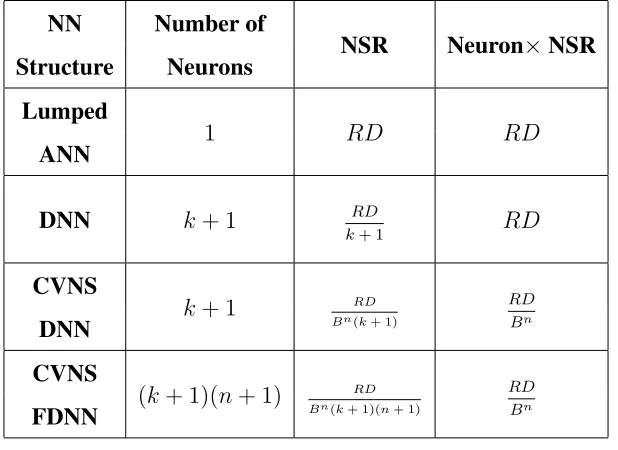
2.2. The number of CVNS digits is equal ton+ 1when applicable.
Table 2.2: Comparison of different sigmoidal Adalines for ak+ 1input
NN Number of
NSR Neuron×NSR
Structure Neurons
Lumped
1 RD RD
ANN
DNN k+ 1 RD
k+ 1 RD
CVNS
k+ 1 RD
Bn(k+ 1)
RD Bn
DNN
CVNS
(k+ 1)(n+ 1) RD
Bn(k+ 1)(n+ 1)
RD Bn
FDNN
There is a tradeoff between the number of neurons and the value of NSR in distributed
neural networks. To measure the overall efficiency of each network in Table 2.2, a
com-parison factor, Neuron×NSR, is defined which is the result of multiplying the number of
neurons by NSR for each structure. It is shown that the proposed networks outperform the
other two networks due to their smaller Neuron×NSR values.
2.6 Conclusion
Two novel CVNS Distributed Neural Networks are proposed. They have the self-scaling
structures are compared to those of lumped neural networks and conventional distributed
neural networks. It is shown that significant improvements are attained specially as the
number of inputs increases. The proposed CVNS DNN can defeat both lumped ANN and
conventional DNN with its low NSR while it uses the same number of neurons as the latter
Truncated CVNS Distributed Neural
Network
the CVNS has been used to build a new family of distributed neural networks [16] where
it is used in a high resolution environment. The CVNS DNN was shown to provide a
NSR lower than that of the conventional DNNs. However, practical implementation of
the CVNS systems is limited by the resolution of the environment. For example, a CVNS
digit which is extracted from 12binary bits needs at least a reliable12-bit resolution for
hardware implementation, which is not the case in generally using technologies.
Truncation methods are applied to the CVNS digits to make them cope with lower
resolution environments while still keeping the CVNS properties such as the redundancy
between digits [14, 15]. One of the advantages of applying these methods is reducing the
area consumption; however, it may result in lower accuracy as well.
Here, the CVNS DNN is studied according to the environmental considerations. The
per-formed on the accuracy and the NSR of the proposed truncated CVNS DNN for an
envi-ronment with the reliable resolution of4-bit. Studies show that the NSR is higher than the
NSR of the complete CVNS DNNs, as expected; however, it is still less than that of the
conventional DNNs.
3.1 Truncated CVNS DNN
The acceptable resolution for0.18µmCMOS technology using a power supply voltage of
1.8V is considered to be4-bit [15]. As a result, all arithmetic operations are assumed to be
correct up to4bits, and additional values may need to be checked and corrected.
The first truncation is applied to the number of bits which are used to generate each
CVNS digit. This number of bits is called group length and is selected as4for the sake of
the practical resolution. In other words, in this work, each CVNS digit is generated from
up to4bits.
Another flexible parameter in the CVNS digit sets is called digit link which is the
num-ber of common bits used to generate the CVNS digits. Keeping the digit link in its
maxi-mum means that the number of the CVNS digits and the binary digits are exactly the same
when the radices are equal as is shown in equation (3.1); there will be 13 CVNS digits
equivalent to13bits. This will increase the number of partial multiplications and additions
and consequently the complexity of the system.
((w))n−j|l,t = mX−j
i=0
wi·2i+j−m, j = 0,1, ..., n (3.1)
To overcome this problem, digit link is decreased to its minimum which is equal to
1. This reduces the redundancy as well as the noise immunity of the digits. However, a
proper design of the CVNS generation module will suppress this problem; error correction
is generally performed over digits in a CVNS generation module [13].
length of4and digit link of1[15].
((w))n−j =
m−Xj(4−1)
i=m−j(4−1)−4+1
wi·2i+j(4−1)−m, j = 0,1, ..., n (3.2)
wherewishows theithbit in binary representation.
There is a relation between the number of binary digits,m+ 1, and the number of the
CVNS digits,n+ 1, as follows.
n+ 1 =R( m+ 1
group length−digit link) (3.3)
whereRis the classical Rounding function.
Using the CVNS digit set generated from equation (3.2) as the multiplicand, the CVNS
multiplication equation is no longer applicable. This equation needs the maximum link
between digits as well as the maximum group length to be adjusted.
A new method is proposed to perform the multiplication over the truncated CVNS
digits. Here, the proposed multiplication method is particularized for a case that the
multi-plicand is a CVNS digit set with4CVNS digits,((x))i (i= 3, ...,0), and the multiplier has
4bits,(Z)i (i= 4, ...,1). The radix of the CVNS system is equal to2.
First, four partial results,yi (i= 3, ...,0), are generated.
y3 = ((w))3×
1
X
i=4
(Z)i 2i−4
y2 = (((w))2mod1)× 1
X
i=4
(Z)i2i−4
y1 = (((w))1mod1)× 1
X
i=4
(Z)i2i−4
y0 = (((w))0mod1)× 1
X
i=4
(Z)i2i−4 (3.4)
Themod1shows the modulo1operation and is applied as there is1digit link between
y1, andy0; therefore, it prevents the double effect of the common digit in the final result.
It should be noted that finally the partial results are added up together to generate the final
synapse output.
Note that the partial results are not in the CVNS form as there is no longer any overlap
between them; they are just continuous values equivalent to8bits.
There is one total output for the synapse; thus, these partial results are scaled and added
up together as follows.
y= ((y0×2−3+y1)×2−3+y2)×2−3+y3 (3.5)
However, there are some practical limitations applied to equations (3.4) and (3.5)
be-cause of the resolution of the environment. These are discussed through the following case
study.
Case study 1: The randomly chosen value for multiplicand is ‘0111,1101,0101,1’, and
the multiplier is chosen equal to ‘1110’. The CVNS digits for the multiplicand are extracted
using equation (3.2): [0.875, 1.75, 0.625, 1.375]. The partial results are calculated through
equation (3.4) as is shown in Table 3.1.
The first columns in Table 3.1 shows the partial results in a high resolution
environ-ment. The results in an environment with4-bit resolution are shown in the second columns.
They are rounded values of the previous column. Therefore, the classic Rounding function
should be added for partial results extractions in equation (3.4) for hardware
implementa-tions.
The lower resolution environment also has an effect on equation (3.5). According to
equation (3.5), the final output in the high resolution environment is found as shown in
Figure 3.1 which is equal to ‘0110,1101,1010,1101,0’,6.8547in decimal.
In a 4-bit resolution environment, the classic Rounding function should be added for
each scaling addition in equation (3.5). Consequently, each7-bit result will be rounded to
Table 3.1: Multiplication partial results forcase study 1.
High Resolution Low Resolution
Partial Result Equivalent Bits Partial Result Equivalent Bits
y3= 1.53125 0110,0010 y3= 0.75 0110
y2= 1.3125 0101,0100 y2= 0.625 0101
y1= 1.09375 0100,0110 y1= 0.5 0100
y0= 0.65625 0010,1010 y0= 0.375 0011
0 1 1 0 0 0 1 0
0 1 0 1 0 1 0 0
0 1 0 0 0 1 1 0
0 0 1 0 1 0 1 0
+
+
+
0 1 1 0 1 1 0 1 1 0 1 0 1 1 0 1 0
Figure 3.1: Final multiplication result in a high resolution environment.
Figure 3.2 shows the multiplication process in a 4-bit resolution environment. The
result,‘0111’ (7in decimal), is the rounded value of the result in Figure 3.1.
From Figure 3.2, the effect of the lower index digits is contributed to the highest index
digits. Without this, the output would be only calculated from the first CVNS digit resulting
in ‘0110’ (6in decimal) which is far from the right answer.
The proposed truncated CVNS DNN is used to build a2−2−1XOR with sigmoidal