Verification Environment of GPIO Core
using UVM and Makefile in Perl Scripting
Salma Jabeen1, Asarafuddin M D2
Assistant Professor, Dept. of ECE, GNIT, Hyderabad, Telangana, India1
Team Lead in private forum, Hyderabad, Telangana, India2
ABSTRACT:The GPIO core design provides a general purpose input/output interface to a 32-bit On-Chip Peripheral
Bus (OPB). GPIO is a generic pin on an integrated circuit (IC) whose behavior, including whether it is an i/o pin, that can be controlled by the user at run time. Almost all FPGA boards contain GPIO peripheral. In this paper we have tried to implement GPIO design by writing the code in VERILOG and simulating it in QUESTA MODELSIM and writing makefile in perl scripting and verifying all functions of GPIO core by UVM. The functional and code coverage and functional verification of the GPIO RTL design is carried out for the better optimum design.
KEYWORDS: GPIO, OPB,Perl Scripting, QUESTA MODELSIM, XILINX ISE, Verilog, UVM, Coverage, FPGA
I. INTRODUCTION
The General purpose input/output IP core is user-selectable or user-programmable general-purpose Input/output controller. It is mainly used for implementation of functions that are not implemented with help of dedicated controllers in a system and require simple output and input software controlled or programmable signals. The General Purpose IO module is part of Inicore's IP module family. This general purpose input/output controller gives some unique features that ease system integration and use. Each General Purpose IO port can be configured for output input or bypass mode. In one set all output data can be access. Single or multiples bits can be cleared or set independently. Every General Purpose IO port can serve as an interrupt source and has its own configuration options: • Level sensitive, single edge triggered or level change • Active low or high respectively positive edge or negative edge. • Individual interrupt enable register and status flags. The GPIO core provides several synthesis options to ease the system integration and minimize the gate count: •CPU bus width is selectable: default options are 8/16/32-bit • Selectable number of General Purpose I/O ports • CPU read back enable
II. GPIO (GENERAL PURPOSE I/O)
General architecture of GP I/O IP core is consists of four main building blocks: • APB host interface
• GP I/O registers • Auxiliary inputs
A. Architecture of GPIO
Fig.1 Architecture of GPIO
i. Clocks: The GP I/O core has two clock domains. All registers are in system clock domain except RGPIO_IN. The
register RGPIO_IN can be clocked by external clock or by system clock.
ii. APB Interface: APB interface connects GPIO core to the host system.The implementation implements a 32-bit bus
width and does not support other bus widths.
iii. GPIO Registers: The GP I/O IP Core has several software accessible or programmable registers. Most registers have the same width as number of general-purpose I/O signals and they can be from 1 – 32 bits. The host through these registers programs type and operation of each general-purpose I/O signal
iv. Auxiliary Inputs: The auxiliary inputs can bypass RGPIO_OUT outputs based on programming of RPGIO_AUX
register. Auxiliary inputs are used to multiplex other on-chip peripherals on GPIO pins.
v.Interface to External I/O Cells and Pads: External interface connects GPIO core to external I/O ring cells and pads.
To support open-drain or three-state outputs, appropriate opendrain or three-state I/O cells must be used. Part of external interface is also ECLK signal. It can be used to register inputs based on external clock reference.
III. UNIVERSAL VERIFICATION METHODOLOGY
The UVM (Universal Verification Methodology) was introduced in December 2009, by a technical Sub committee of Accellera. The Universal Verification Methodology (UVM) is a standardized methodology for verifying integrated circuit designs. UVM is derived mainly from the OVM (Open Verification Methodology) which was, to a large part, based on the eRM (e Reuse Methodology) for the e Verification Language developed by Verisity Design in 2001. The UVM class library brings much automation to the SystemVerilog language such as sequences and data automation features (packing, copy, compare) etc., and unlike the previous methodologies developed independently by the simulator vendors, is an Accellera standard with support from multiple vendors: Aldec, Cadence, Mentor Graphics, and Synopsys.
Today, more and more logic is being integrated on the single chip so verification of it is a very challenging task. More than 70 percent of the time is spent on the verification of the chip. So it is a need of an hour to have a common verification methodology that provides the base classes and framework to construct robust and reusable verification environment. UVM provides that.
IV. UVM TESTBENCH ARCHITECTURE
The following subsections describe the components of a verification . • Data Item (Transaction)
• Driver (BFM) • Sequencer • Monitor • Agent • Environment
• Data Item (Transaction): Data item are basically the input to the device under test. All the transfer done between
different verification components in UVM is done through transaction object. Networking packets, instructions for processor are some examples of transactions.
• Driver (BFM): Driver as the name suggest, drive the DUT signals. It basically receives the transaction object from
the sequencer and converts it in to the pin level activity. So for example it can generate read or write signal, write address and data to be transferred. It is the active part of the verification logic.
• Sequencer: Sequencer is the component on which the sequences will run. The DUT needs to be applied a sequence of
transaction to test its behaviour. So sequence of transaction is generated and it is applied to driver whenever it demands by the sequencer.
• Monitor: A monitor is the passive element of the verification environment. It just sample the dut signal from the interface but does not drive them. It collect the pin information, package it in form of a packet and then transfer it to scoreboard or other components for coverage information.
• Agent: Agent is basically a container. It contains driver, monitor and sequencer. Driver and sequencer are connected
in agent. Agent has two modes of operation: passive and active. In active mode it drives the signal to the DUT. So driver and sequencer are instantiated in active mode. In passive mode it just sample the DUT signals does not drive them. So only monitor is instantiated in passive mode.
• Scoreboard: Scoreboard is a verification component that checks the response from the DUT against the expected
response. So it keeps track of how many times the response matched with the expected response and how many time it failed.
• Environment: Environment is at the top of the test bench architecture, it will contain one or more agents depend on
design. If more than one agents are there then it will be connected in this component. Agents are also connected to other components like scoreboard in this component.
V. PERL SCRIPTING
Perl was originally developed by Larry Wall in 1987 as a general-purpose Unix scripting language to make report processing easier.The Perl languages borrow features from other programming languages including C, shell script (sh), AWK, and sed.They provide powerful text processing facilities without the arbitrary data-length limits of many contemporary Unix command line tools, facilitating easy manipulation of text files.In addition to CGI, Perl 5 is used for system administration, network programming, finance, bioinformatics, and other applications, such as for GUIs. #!usr/bin/perl – called the "shebang line", after the hash symbol (#) and ! (bang) at the beginning of the line. It is also known as the interpreter directive.
# – the number sign, also called the hash symbol. In Perl, the # indicates the start of a comment. It instructs perl to ignore the rest of the line and not execute it as script code.
VI. RESULTS AND DISCUSSION
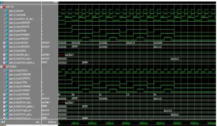
Fig 3. simulation showing GPIO Functional Verification for write operation
The GP I/O is carried out for the functional verification using the UVM technique for both the read and write operation. The functional verification is of the RTL design is of the GPIO is yields the complete code and functional coverage. The GPIO is set up as DUT for the functional verification and the code coverage is obtained for 100%.
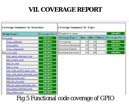
VII. COVERAGE REPORT
Fig 5 Functional code coverage of GPIO
VIII. CONCLUSION
In this we have designed and verified the GPIO core using Verilog and UVM technique using Questasim. The code coverage is obtained for the RTL design and 100% code coverage and functional coverage is extracted. The per scripting is written for makefile.This methodology provides the complete coverage of the RTL design so as to acquire the fault free Protocol design of GPIO. So that can be implemented in real time systems. This can be further implemented for the ASIC implementation and SOC Applications.
REFERENCES
[1] D.Gajski et al, “Essential Issues for IP Reuse”, Proceedings of ASP-DAC, pp.37-42, Jan. 2000
[2] C.K.Lennard et al, “Industrially proving the SPIRIT Consortium Specifications for Design Chain Integration”, Proceedings of DATE 2006, pp. 1-6, March 2006
[3] K.Cho et al, “Reusable Platform Design Methodology For SOC Integration And Verification”, Proceedings of ISOCC 2008, pp. I-78- I-81, Nov. 2008
[4] W.Kruijtzer et al, “Industrial IP integration flows based on IP-XACT standards” proceedings of DATE 2008, pp. 32-37, March 2008
[5] M.Strik et al, “subsystem Exchange in a Concurrent Design Process Environment” Proceedings of DATE 2008, pp. 953-958, March 2008 International Journal of Scientific and Research Publications, Volume 5, Issue 6, June 2015 4 ISSN 2250-3153 www.ijsrp.org
[6]GensysIO,http://www.atrenta.com/solutions/gensysfamily/gensys-io.htm [7] SocratesSpinner
[8] opencores.org [9] http://testbench.in