Common-Mode Suppression in Broadside Coupled Coplanar
Waveguides
Yujie He1, Joseph M. Faia1, Michael Cracraft2, and Edward Wheeler1, *
Abstract—Differential signaling is used in digital circuitry and high speed communication links due to its lower level of radiation and lower susceptibility to interference. Signal skew, amplitude differences and unequal parasitic electric or magnetic coupling to nearby structures can lead to common-mode signals being present on differential communication links which can result in unwanted electromagnetic interference and crosstalk. Common-mode filtering is often employed to suppress common-mode signal propagation in order to mitigate against these negative effects. In this paper broadside coupled differential coplanar waveguides are used which provide effective differential transmission from dc
through 40 GHz. Simulation and measurement show that dipole-like common-mode filtering elements placed between the broadside coupled traces offer common-mode suppression of more than 10 dB over bandwidths greater than 5 GHz. A design equation is developed which can be used to estimate filtering frequencies from filter dimensions through 30 GHz. Filters can be cascaded to broaden filtering around a single frequency to filter at multiple frequencies. Simulation based registration studies were conducted which show stable filtering performance in the presence of layer-to-layer misregistration up to 0.254 mm.
1. INTRODUCTION
Differential signaling is frequently used in digital circuitry and high speed communication links because of its lower level of radiation and its lower susceptibility to interference. In any practical differential signaling structure, signal skew, amplitude differences and unequal parasitic electric or magnetic coupling to nearby structures can lead to the presence of a common-mode (CM) signal which can, in turn, result in higher levels of electromagnetic interference (EMI) and crosstalk. CM filtering structures can be used in differential transmission lines to suppress common-mode signal propagation, thereby avoiding the negative effects of CM propagation.
Past work to suppress common-mode propagation in microstrip or stripline differential transmission lines has included patterned ground structures [1–5], electromagnetic bandgap structures [6–8], periodic structures [9], and metamaterial inspired structures such as complementary split-ring resonators [5, 10– 13]. Less effort has been directed toward investigating common-mode suppression in differential coplanar waveguides. Table 1 lists transmission line type, filter design, center frequency, and fractional bandwidth for some of the previous work in common-mode filtering along with the results reported here.
In this paper, we investigate effective differential transmission and CM suppression in broadside coupled coplanar waveguides (BC CPWs) which comprise two conventional CPWs, one on top of the other, separated by a dielectric. Earlier work on coupled coplanar waveguides [14], Beldair and Wolff, assuming differential excitation, placed one reference conducting plane at the resulting electric wall shown in Figure 1(a) and added another above the CPW to produce the single-ended structure shown in Figure 1(b). For the resulting single-ended structure, they employed numerical analysis to reveal four limiting cases distinguished by geometry and permittivity.
Received 17 January 2019, Accepted 24 April 2019, Scheduled 25 April 2019
* Corresponding author: Edward Wheeler (wheeler@rose-hulman.edu).
1 Department of Electrical and Computer Engineering, Rose-Hulman Institute of Technology, 5500 Wabash Ave., Terre Haute,
Table 1. Results from current and past work in common-mode filtering.
Transmission line type Filter design Center frequency Fractional BW
broadside-coupled CPW
(results presented here) λ/2 resonator
15 GHz (single filter) 16 GHz (cascade)
42.5% 61.5%
differential microstrip
defected ground structure (DGS)
6.35 GHz [1] 5.4 GHz [3]
87% 130% electromagnetic
bandgap (EBG)
4.95 GHz [6] 14.25 GHz [7]
6.1% (est.) 17.5% (est.)
periodic structures 8 GHz [9] 30% (est.)
CSRR 1.5 GHz [10] 40% (est.)
DS-CSRR 1.5 GHz [10] 43% (est.)
OCSRR 0.9 GHz [11] 73% (est)
differential stripline EBG structures 12.5 and 15.1 GHz [7] 21.4% (est.)
(b) (a)
(d) (c)
Figure 1. (a) Cross-section of the broadside coupled coplanar waveguide with a differential signal and (b) single-ended CPW with reference conductors above and at the electric wall, (c) cross-section of the BC CPW with lateral sidewalls and a conducting plane at the position of the electric wall and (d) cross-section with lateral sidewalls and no conducting plane.
The BC CPWs investigated here — with a relatively large slot width (w) together with no upper conducting plane (ht large) — fall into the fourth case where the flux for a differential signal is largely between the trace and the lower conducting plane (or electric wall in the BC CPW). One therefore would expect little change in the flux structure under differential excitation if a third layer of metallization were placed at the electric wall as shown in Figure 1(c). There would likewise be little variation in the electric flux pattern as the cross-section alternates from that shown in Figure 1(c) to that shown in Figure 1(d) and vice versa.
Even though the presence of the lateral sidewalls cannot be ignored since d is not greater than 8 h [15], the dominant flux for Figure 1(c) is between the traces and the reference layer between them and between the traces for Figure 1(d). This is illustrated in the flux plots in Figures 2(a) and 2(b), which were obtained employing CST Microwave Studio (MWS).
Contrast this with CM excitation applied to the BC CPW shown in Figures 1(c) and 1(d) as illustrated in Figures 2(c) and 2(d). Effective differential-mode (DM) transmission together with CM suppression might therefore be expected since placing a reference plane between the two CPWs alters common-mode flux patterns significantly while altering differential pattern to a much lesser degree.
(a)
(b)
(c)
(d)
Figure 2. All plots obtained using CST MWS, (a) DM flux with conducting reference plane between the traces, (b) DM flux with no reference plane present, (c) CM flux with conducting reference plane between the traces, (d) CM flux with no reference plane present.
a CM signal allows half-wavelength dipole resonant structures in the middle metallization layer to be employed for CM suppression while the absence of net flux from DM signal prevents resonance to allow effective DM transmission. One can enumerate desirable attributes for the BC CPW structure to be useful as a differential communication link. These include i) DM transmission with low attenuation and dispersion, ii) CM filters offering suppression over a wide frequency range, iii) design equations allowing designers to estimate filtering frequencies, iv) relative robust performance in the presence of layer misregistration and v) effective launch structures allowing contacts to be made from one side of the printed circuit board (PCB). In this paper, modeling, simulation, and measurement are used to demonstrate the first four attributes with the fifth pertaining to signal launches from one side of the board remaining for future work.
2. BOARD STACKUP AND FILTER DESIGN
BC CPW waveguides comprising two single-ended CPWs, with vias connecting reference layers to provide lateral sidewalls, are the differential transmission lines used in this investigation. The CM filtering elements considered here are dipole-like resonant structures placed in the middle metallization layer.
Simulation and measurement results demonstrate that this differential transmission line offers CM suppression over wide bandwidths with effective DM transmission fromdc to 40 GHz.
Rogers RO4350B laminates (εr = 3.48 and a loss tangent of 0.0037 at 10 GHz) with bonding
by Rogers 4450F bondply (εr = 3.52 and a loss tangent of 0.004 at 10 GHz). These were also used
in all CST MWS simulations. The lateral sidewall was realized through via fences placed along the CPW transmission line, which have the added benefit of preventing filtered CM energy from exciting parallel-plane waveguide modes [12]. In addition to the 3D modeling, 2D cross-sectional models were constructed. The stackup and dimensions of the printed circuit board (PCB) are shown in Figure 3. Details of the filtering layer (the middle layer of metallization in the stackup) are shown in Figure 4.
The filter behavior can be replicated with transmission line models from cross-sectional analysis. However, in its simplest form, this analysis neglects the effects of the connection between the filter element and the adjacent reference plane. Models are developed for the CM filtering elements, which allow the filtering frequencies to be predicted using a simple design equation for frequencies through 30 GHz.
h=0.
s=0.
254, hl=0.168
536, w=0.443
8,ct=0.043,bt
(all dimensio
t=0.096
ons in mm)
lengtth=50, width==6
(a)
(b) (c)
Figure 3. (a) Cross-section view of the PCB, bonding film shown in white, (b) top view, identical to the bottom view, (c) close-up perspective view.
(a) (b)
Figure 4. (a) Filter layer (middle layer metallization) and (b) Close-up view of a the filter structure.
Sign
Sign
Refe nal 1
nal 2
erence
Filterr
fl/2 fl/2
(a) (b)
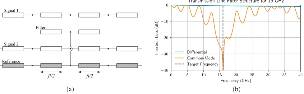
Figure 5. (a) Transmission line approximation with no parasitics, (b) differential and common-mode insertion loss responses for the transmission line model of the broadside coupled filter represented in Figure 5.
similar to Figure 3(a), the via wall is represented as a solid vertical connection between the reference planes, which helps justify treating the references as a single conductor in this simplified model. A fourth line was introduced to the model in the filtering region. The connection between center of the filter element and the reference was approximated a lumped short (no parasitics represented).
leads tof l= 5.03 mm. The three-line structures stretch the rest of the 50 mm length.
Figure 5(b) shows the insertion loss for both modes. The differential is unperturbed while the common-mode experiences a large amount of loss over a wide band centered around 16 GHz.
For f l sw, one can estimate the filtering frequency by taking f l as one-half wavelength at the desired CM filtering frequency. As f l decreases, sw and even f w amount to a significant amount of electrical length. Therefore, expression forf l must be amended to account for the electrical length of the shorting connection and the width of the filter patch itself.
leff
2 =sw+
f l
2 +
f w
2 =n
λ
4 n= 1,3, . . . (1) The resulting design Equation (1) effectively estimates CM filtering frequencies for the PCB stackup employed here through 30 GHz, as will be demonstrated in Section 3. We have performed parameter sweeps to demonstrate that the differential CPW waveguide’s transmission and CM filtering is maintained in the presence of moderate levels of layer-to-layer misregistration.
3. MEASUREMENT AND RESULTS
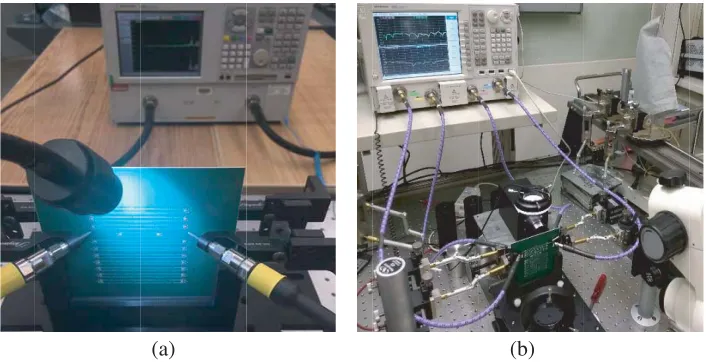
Measurements were carried out at two facilities on two different samples. At the first facility, shown in Figure 6(a), two 500µm GGB RF probes are connected to an Agilent E8363B 40 GHz 2-port VNA through 2.92 mm cables. Additional GGB RF probes with 50 Ω broadband loads are connected to unused ports for each 2-port measurement with SOLT calibration performed at the end of the cables. Measurements conducted at the second facility, shown in Figure 6(b), employed an Agilent N5242A 4-port 26.5 GHz VNA with 2.92 mm cables and GGB RF probes. The same calibration technique is performed before measurements.
(a) (b)
Figure 6. (a) PCB measurement setup with a 2-port VNA. The broadband 50 Ω loads are on the other side of the test board, (b) PCB measurement setup with a 4-port VNA.
3.1. Filtering at a Single Frequency
A differential CPW structure with a single filtering structure as illustrated in Figure 5 was investigated first. The structure dimensions were designed for CM filtering at 16 GHz using design Equation (1). Measurement results are shown together with simulation in Figure 7. The simulated−10 dB bandwidth is 6.14 GHz and is centered at 15 GHz, demonstrating CM filtering over a broad band.
Magnitude (dB)
-60 -60
0 10 20 30 40 0 10 20 30 40
(a) (b)
Figure 7. (a) Measured and simulated transmission DM and CM transmission for a differential CPW structure with a single 16 GHz filter, (b) de-embedded measured and simulated results for a single 16 GHz filter (note 0–26.5 GHz frequency range).
(a)
(b)
Figure 8. (a) Response showing effective transmission for a pure differential signal, (b) response showing the common-mode filtering.
Figure 8 illustrates field simulations of the waveguide with a common-mode filter present. Figure 8(a) shows the electric field when the 15 GHz signal is a pure differential signal, clearly showing effective propagation of the differential signal. Figure 8(b) shows the response the signal is pure common mode (note that Scc21 at 15 GHz is approximately −32 dB) showing the effectiveness of the
common-mode filter.
3.2. Filtering at Multiple Frequencies
Figure 9. Cascade of two filtering structures, the larger (highlighted) designed for 16 GHz and the smaller designed for 32 GHz. Dimensions for 16 GHz filter (in mm): f l= 3.698,f w= 0.536,sw= 0.443,
sl= 0.125. Dimensions for 32 GHz filter (in mm): f l= 1.090, f w= 0.536, sw = 0.443, sl= 0.125 mm.
Magnitude (dB) Magnitude (dB)
-80 -80
0 10 20 30 40 0 10 20 30 40 Frequency (GHz) Frequency (GHz)
(a) (b)
Figure 10. Measured and simulated transmission results for cascaded 16 and 32 GHz filter structure, (a) used in simulation and (b) εr = 3.66 used (obtained by Rogers through averaging over several lots
of laminate material).
with each is the measured filtering frequencies of 14.07 GHz and 28.64 GHz with 10 dB bandwidths of 8.175 GHz and 14.61 GHz, respectively.
3.3. Registration Study
In multilayer PCB fabrication processes, robust performance in the presence of moderate layer-to-layer misregistration is important if one is to avoid system performance being compromised by manufacturing tolerances. Previous researchers observed that misregistration can be a significant source of DM to CM conversion [18]. The parameter sweeps illustrated in Figure 12 demonstrate the differential CPW waveguide’s transmission, and CM filtering is maintained in the presence of moderate levels of layer-to-layer misregistration.
-10
0 10 20 30 40 50 -800 10 20 30 40 50
(a) (b)
Figure 12. Simulated results of the registration study: (a) differential mode signal transmission; (b) common mode signal transmission.
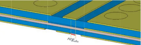
The distance from the center of the transmission line to the vertical center axis of the board (reg) was swept from 0 to 5 mils. In each simulation, the top and bottom signal lines move this distance from the center in opposite directions so that the trace-to-trace misregistration, as illustrated in Figure 11 and denoted as regabs, is twice the value of reg shown in Figure 11. The plots in Figure 12 show that these designs maintain robust performance in the presence of moderate misregistration, here demonstrated to 10 mils or 0.254 mm.
4. CONCLUSIONS
In this paper modeling, simulation, and measurement have been employed in an investigation of CM filtering in BC CPW structures. Results indicate that BC CPW with dipole-like resonant structures placed in the metallization layer between the traces offers effective DM transmission from dc through 40 GHz and at least 10 dB in CM attenuation over bandwidths greater than 5 GHz. A design equation was developed for the synthesis of filter elements, and simplified transmission line models were included to illustrate the relationship to the structure’s dimensions. The filtering elements can be cascaded to filter at multiple frequencies or to broaden the filtering bandwidths. Registration studies are provided in which simulations show stable filtering performance in the presence of layer-to-layer misregistration up to 0.254 mm.
Future work includes development of launch structures to permit signal launch from a single side of the board including multiple, closely spaced launches to allow the analysis of possible effects of cross-talk. A second interesting area of investigation would be to investigate BC CPWs with smaller geometries since previous work with single-ended CPWs with lateral sidewalls demonstrated effective transmission to 500 GHz [19].
REFERENCES
1. Wu, S.-J., C.-H. Tsai, T.-L. Wu, and T. Itoh, “A novel wideband common-mode suppression filter for gigahertz differential signals using coupled patterned ground structure,” IEEE Trans. Microw. Theory Techn., Vol. 57, 848–855, Apr. 2009.
2. Liu, W.-T., C.-H. Tsai, T.-W. Han, and T.-L. Wu, “An embedded common-mode suppression filter for GHz differential signals using periodic defect ground plane,”IEEE Microw. Wireless Compon. Lett., Vol. 18, 248–250, May 2008.
4. Liu, Q., G. Li, V. Khilkevich, and D. Pommerenke, “Common-mode filters with interdigital fingers for harmonics suppression and lossy materials for broadband suppression,” IEEE Trans. Electromagn. Compat., Vol. 57, 1740–1743, Dec. 2015.
5. Mart´ın, F., J. Naqui, A. Fern´andez-Prieto, P. V´elez, J. Bonache, J. Martel, and F. Medina, “The beauty of symmetry,” IEEE Microw. Mag., 42–55, Jan./Feb. 2017.
6. De Paulis, F., L. Raimondo, S. Connor, B. Archambeault, and A. Orlandi, “Design of a common-mode filter by using planar electromagnetic bandgap structures,” IEEE Trans. Adv. Packag., Vol. 33, 994–1002, Nov. 2010.
7. De Paulis, F., M. Cracraft, D. Di Febo, M. H. Nisanci, S. Connor, B. Archambeault, and A. Orlandi, “EBG-based common-mode microstrip and stripline filter design: Experimental investigation of performances and crosstalk,” IEEE Trans. Electromagn. Compat., Vol. 57, 996–1004, Oct. 2015. 8. Kodama, C., C. O’Daniel, J. Cook, F. de Paulis, M. Cracraft, S. Connor, A. Orlandi,
and E. Wheeler, “Mitigating the threat of crosstalk and unwanted radiation when using electromagnetic bandgap structures to suppress common mode signal propagation in PCB differential interconnects,” Proc. IEEE Int. Symp. Electromagn. Compat., 622–627, Dresden, Germany, Aug. 2015.
9. Cracraft, M. and S. Connor, “Mode-selective periodic transmission line filters to reduce radiated common-mode emissions,” Proc. IEEE Int. Symp. Electromagn. Compat., 216–221, Ottawa, Canada, Jul. 2016.
10. Naqui, J., A. Fern´andez-Prieto, M. Dur´an-Sindreu, F. Mesa, J. Martel, F. Medina, and F. Mart´ın, “Common-mode suppression in microstrip differential lines by means of complementary split ring resonators: Theory and applications,” IEEE Trans. Microw. Theory Techn., Vol. 60, 3023–3034, Oct. 2012.
11. Velez, P., J. Naqui, A. Fern´andez-Prieto, M. Dur´an-Sindreu, J. Bonache, J. Martel, F. Medina, and F. Mart´ın, “Differential bandpass filter with commo-mode suppression based on open split ring resonators and open complementary split ring resonators,”IEEE Microw. Wireless Compon. Lett., Vol. 23, 22–24, Jan. 2013.
12. Sawyer, E., C. Kodama, C. O’Daniel, J. Cook, and E. Wheeler, “Using common-mode filtering structures with microstrip differential lines in a multilayer printed circuit board environment,”
IEEE European Microw. Conf., 1091–1094, Rome, Italy, Oct. 2014.
13. He, Y., Z. Silva, Z. Bergstedt, J. Faia, S. Van Hoosier, S. G. Kang, G. Shaffer, E. Wheeler, and M. Cracraft, “Common-mode filtering in multilayer printed circuit boards,”Proc. IEEE Int. Symp. Electromagn. Compat., 288–292, Washington, DC, USA, Aug. 2017.
14. Bedair, S. S. and I. Wolff, “Fast and accurate analytic formulas for calculating the parameters of a general broadside-coupled coplanar waveguide for (M)MIC applications,” IEEE Trans. Microwave Theory Tech., Vol. 37, 843–850, May 1989.
15. Kretch, B. and R. Collin, “Microstrip dispersion including anisotropic substrates,” IEEE Trans. Microwave Theory Tech., Vol. 35, 710–718, Aug. 1987.
16. Keysight Technologies, Santa Rosa, CA, USA. Auto Fixture Removal (AFR), (2015) [Online], Avail-able: http://na.support.keysight.com/plts/help/WebHelp/VNACalAndMeas/Auto Fixture Remo-val.htm, Accessed on: Apr. 20, 2018.
17. Keysight Technologies, Santa Rosa, CA, USA. Auto Fixture Removal (AFR), (2014) [Online], Available: http://na.support.keysight.com/vna/help/latest/S3 Cals/Auto Fixture Removal.htm, Accessed on: Apr. 20, 2018.
18. Shan, L., Y. Kwark, C. Baks, and M. Ritter, “Layer misregistration in PCB and its effects on signal propagation,” Proc. Electronic Components and Techn. Conf., 605–611, Las Vegas, NV, USA, Jun. 2010.