Graph-Based Transistor Network Generation Method for
Supergate Design
Guttula Dharmaraju & M. Srinivasulu
1M.tech-Scholar, Dept of ECE, Amalapuram Institute of Management Sciences and college of
Engineering, Mummidivaram, A.P.
2HOD & Associate Professor, Dept of ECE, Amalapuram Institute of Management Sciences and college of
Engineering, Mummidivaram, A.P
ABSTRACT: Optimizing transistor network represents an efficient way of improvising VLSI circuits. Existing optimization methods are not actually the most effective way to generate optimized network. The method of reducing only number of literals in a given Boolean expression does not actually reduce the transistor count. This paper proposes a graph-based method for minimizing the number of transistor count that compose a network. This proposed method can provide networks with minimum transistor count with irredundant sum-of-products expression as the input. Experimental results produced by the proposed method shows a substantial reduction in the number of transistor used in the networks. Keywords: Digital circuit, factorization, graph theory, transistor network.
I. INTRODUCTION
In digital VLSI design the power dissipation and area of circuits are mainly related to the number of transistors used in the circuit. Hence, transistor network optimization is an efficient way when designing custom gates to be used in the libraries. Numerous methods have been proposed in the literature for generating and optimizing transistor networks. The most basic method used for transistor network optimization is factoring the Boolean expressions where only series– parallel (SP) transistor network can be produced. On the contrary, graph-based methods can produce both Series-Parallel and non-Series-Parallel (NSP) structures which can provide considerable amount of transistor count reduction.
Reducing the number of literals in Boolean expressions does not actually provide the most efficient transistor networks. Hence, existing factorization methods and graph-based methods may not be able to reduce the transistor count to a greater extent. The way of decreasing the transistor count in logic gates leads to reduction in circuit area and power consumed in digital logic circuits.
In this paper, we propose a method for enhancing the reduction of transistors using both series-parallel (SP) and non-SP (NSP) arrangements that performs OR and AND operations. Using only graph-based methods can reduce the transistor count upto a certain limit. In this paper, we propose a graph-based method followed by
efficient factorization method which
enhance the transistor network to reduce the transistor count to greater extent than other existing optimization techniques.
II. TRANSISTOR NETWORK TO MULTIGRAPH
special vertices (this information is necessary in the proposed algorithm). In the graph theory point-of-view, the correct term for the graph obtained from this
operation is multigraph. The term
multigraph refers to a graph in which
multiple edges between nodes are
permitted. Some references require that multi graph possess no graph loops, while other ones explicitly allow them. For the purpose of this work, the multi graph will not possess graph loops, because in transistor networks there is no transistor connecting the same node. This situation would be a short-circuit in the network.
Another important concept to be
understood is related to the graph planarity. A graph is planar if it can be drawn in a plane without graph edges crossing. This characteristic is required for the dual graph generation. Only planar graphs may deliver a dual graph. In the literature, some algorithms to generate dual graph from a simple graph are available, as presented. In this approach, the ‘exterior’ face is converted to a single vertex in the dual graph.
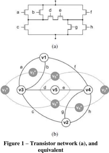
However, for the electrical engineering purpose, the exterior face must be considered as two vertices. For the purpose of this work these vertices are called exterior vertices. This assumption is necessary since electrical networks are composed by two terminal nodes. Fig. 1a illustrates a transistor network, and Fig. 1b shows a planar multigraph obtained from this network and its two exterior vertices dual graph (dotted lines). In the case of generating a dual graph from a simple
graph, all edges joining to the vertex V1*
(as illustrated in Fig. 1b) should be
redirected to vertex V2*. The vertex V1*
would be suppressed. Apart from that, it is important to notice that a simple graph does not allow multiple edges between two
same vertices, like the edges joining V1
and V3 in Fig. 1b.
Since simple graph and multigraph are not sufficient to meet the requirements to generate a dual two terminal transistor network, this structure of multigraph with two exterior vertices is presented as an adequate solution.
Figure 1 – Transistor network (a), and equivalent
multigraph (b) representation and its dual (doted lines).
III. PROPOSED SYSTEM
The proposed method comprises two main modules: 1) the kernel identification and 2) the switch network composition. The
former receives an ISOP F and identifies
representing subfunctions of f. The latter composes those networks into a single network by performing logic sharing. The provided output is an optimized switch
network representing the target function f.
The execution flow of the method is presented in Fig. 2.
Fig. 2. Execution flow of the proposed method
Initially, we apply the NSP Finder procedure over F in order to find partial transistor networks. Cubes used to achieve such a network structure are removed from F. This removal leads to a simpler ISOP F1. Now the SP Finder procedure is performed over F1 in order to find any SP transistor networks. Cubes used to achieve such a network structure are removed from F1. This removal leads to a simpler ISOP F2. In this order, we apply the algebraic Factorization over F2 to produce factored forms that improves the transistor count
reduction. Finally, the Network
Composition step receives the partial networks and comprises them into a single
network by applying edge-sharing
technique.
Another important aspect is that the proposed graph based method can either enable or disable one of the following
steps NSP Finder, SP Finder,
Factorization. As the proposed approach is
heuristic, it is appropriate to try the three combinations to enable or disable these steps and select the best network among them.
Non- Series-Parallel Finder:
In order to identify Non- Series-Parallel
network structures, the combination of m
cubes are taken four at a time. The method
tries to generate network for each
combination of four cubes.
Factorization:
This section presents a empirical approach to perform naïve algebraic factorizations to the Boolean function considering a constraint to prioritize factorizations that improves the transistor count reduction. In the proposed approach, cubes that share minimum of two literals is taken. For instance, consider the matrix which is obtained from the Boolean function.
Network Composition:
This Network Composition module is used to combine partial network structures generated during previous steps in order to construct the final network. This step receives the logic function F and a list of partial transistor networks from previous steps and combine them into a single network structure. All the partial networks are generated by the NSP Finder, SP Finder and Factorization steps. The final network is produced by combining all the partial networks in parallel then a logic sharing is performed to remove redundant terms.
The simple sharing step performs the edge sharing technique presented. Actually, the method pass through the transistor network structure searching for similar transistors. The network is then restructured so that only one common node is between similar transistors. In some cases, the similar transistors must be exchanged in the network structure in order to share a common node.
Complex Sharing:
The complex sharing step receives the network structure from the previous step
and attempts to perform further
optimizations. Few times, where a
common node is not directly found due to the position of the transistors in the network. In order to improve the switch
sharing, direct Series-Parallel
compressions are performed. A fascinating characteristic of the proposed method is that it can find and generate Series-Parallel and Non-Series-Parallel network structures by applying logic sharing. In few cases, Non- Series-Parallel structures produces significant reduction in the final transistor count.
IV. RESULTS
Fig 3. Output
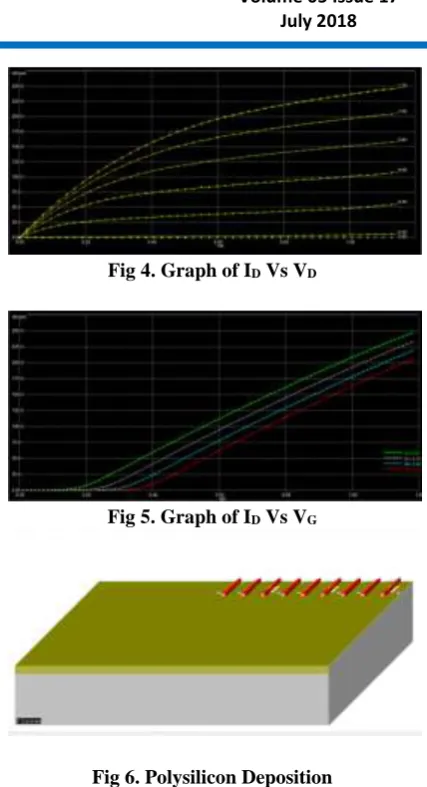
Fig 4. Graph of ID Vs VD
Fig 5. Graph of ID Vs VG
Fig 6. Polysilicon Deposition
Fig 7. End of The Process
V. CONCLUSION
A dual transistor network generation algorithm was presented. The algorithm is a graph-based solution that is able to generate dual networks for bridge-based arrangements. The results show the
demonstrating that it could be used as a later optimization step to achieve efficient transistor networks. The elements count is minimized by exploring this approach, leading to logic cell implementation with small area overhead.
VI. REFERENCES
[1] Y.-T. Lai, Y.-C. Jiang, and H.-M. Chu,
“BDD decomposition for mixed
CMOS/PTL logic circuit synthesis,” in
Proc. IEEE Int. Symp. Circuits Syst.
(ISCAS), vol. 6. May 2005, pp. 5649–
5652.
[2] H. Al-Hertani, D. Al-Khalili, and C. Rozon, “Accurate total static leakage current estimation in transistor stacks,” in
Proc. IEEE Int. Conf.Comput. Syst. Appl.,
Mar. 2006, pp. 262–265.
[3] T. J. Thorp, G. S. Yee, and C. M. Sechen, “Design and synthesis of dynamic
circuits,” IEEE Trans. Very Large Scale
Integr. (VLSI) Syst., vol. 11, no. 1, pp.
141–149, Feb. 2003.
[4] A. I. Reis and O. C. Andersen, “Library sizing,” U.S. Patent 8 015 517, Jun. 5, 2009.
[5] R. Roy, D. Bhattacharya, and V. Boppana, “Transistor-level optimization of
digital designs with flex cells,” Computer,
vol. 38, no. 2, pp. 53–61, Feb. 2005. [6] M. Rostami and K. Mohanram,
“Dual-vth independent-gate FinFETs for low
power logic circuits,” IEEE Trans.
Comput.-Aided Design Integr. Circuits
Syst., vol. 30, no. 3, pp. 337–349, Mar.
2011.
[7] M. H. Ben-Jamaa, K. Mohanram, and G. De Micheli, “An efficient gate library
for ambipolar CNTFET logic,” IEEE
Trans. Comput.-Aided Design Integr.
Circuits Syst., vol. 30, no. 2, pp. 242–255,
Feb. 2011.
[8] M. C. Golumbic, A. Mintz, and U. Rotics, “An improvement on the complexity of factoring read-once Boolean
functions,” Discrete Appl Math., vol. 156,