A depth-16 circuit for the AES S-box
Joan Boyar∗ [email protected]
Ren´e Peralta† [email protected]
Abstract
New techniques for reducing the depth of circuits for cryptographic applications are described and applied to the AES S-box. These techniques also keep the number of gates quite small. The result, when applied to the AES S-box, is a circuit with depth 16 and only 128 gates. For the inverse, it is also depth 16 and has only 127 gates. There is a shared middle part, common to both the S-box and its inverse, consisting of 63 gates.
Keywords: AES; S-box; finite field inversion; circuit complexity; circuit depth.
1
Introduction
Constructing optimal combinational circuits is an intractable problem under almost any meaningful metric (gate count, depth, energy consumption, etc.). In practice, no known techniques can reliably find optimal circuits for functions with as few as eight Boolean inputs and one Boolean output (there are 2256such functions). Thus, heuristic or specialized techniques are necessary in practice.
Recently, Nogami et.al. [10] presented a technique for reducing circuit depth in the for-ward direction of the AES S-box. Their technique was primarily to choose mixed bases for the tower-of-fields architecture in such a way that the matrices doing the linear transforma-tions at the top and bottom had at most 4 ones in every row. In this way they were able to compute these transformations in depth 2 each, for a total of depth 4. Their technique cannot be simultaneously applied to the AES circuit in the reverse direction, as the inverse matrices do not have at most 4 ones in every row. We present more general techniques that are less dependent on the actual representation of the fields. These techniques allow us to produce circuits which are both smaller and shorter in both directions. Although the size of our construction is larger than the one reported in [1], which had only 115 gates, it is comparable to previous efforts to make a compact circuit (see [3, 8]). The latter two constructions have depths between 25 and 27. Nogami et. al. improved this, for the forward direction of the S-Box, to depth 22 at the cost of increasing size to 148. Our new circuits have depth 16 in both directions, size 128 in the forward direction, and size 127 in the reverse direction. The part that is shared between the forward and reverse directions is of size 63.
∗
Department of Mathematics and Computer Science, University of Southern Denmark. Partially sup-ported by the Danish Natural Science Research Council (SNF). Some of this work was done while visiting the University of California, Irvine.
†
2
Combinational circuit optimization
Many different logically complete bases are possible for circuits. Since the operations in the basis (XOR, AND) are equivalent to addition and multiplication modulo 2 (i.e., in
GF(2)), much work on circuits for cryptographic functions uses this basis. For logical completeness, the negation operation (or the constant 1) is needed as well. In GF(2), negation corresponds to x+ 1. For technical reasons, and for an accurate gate-count, we use XNOR gates (XN OR(x, y) = x+y+ 1 in GF(2)) instead of negation. Components free of AND gates are calledlinear; our emphasis is on these components, thoughnonlinear
components are also optimized.
Under the basis (XOR,XNOR,AND), classic results by Shannon [12] and Lupanov [7] show that almost all predicates on n bits have circuit complexity about 2nn. The multi-plicative complexity of a function is the number of AND gates necessary and sufficient to compute the function. Analogous to the Shannon-Lupanov bound, it was shown in [2] that almost all Boolean predicates on n bits have multiplicative complexity about 2n2. Strictly
speaking, these theorems say nothing about the class of functions with polynomial circuit complexity. However, it is reasonable to expect that, in practice, the multiplicative com-plexity of functions is significantly smaller than their Boolean comcom-plexity. This is one of the principles that guide our design strategy.
Circuits with few AND gates will naturally have large sections which are purely lin-ear. Boyar and Peralta [1] have used this insight to construct circuits much smaller than previously known for a variety of applications (see http://cs-www.cs.yale.edu/homes/ peralta/CircuitStuff/CMT.html). The heuristic is a two-step process which first reduces multiplicative complexity and then optimizes linear components.
The work presented in this paper is based on the idea that a short circuit may be obtained by starting from a small (i.e. optimized for size) circuit and performing three types of depth-decreasing optimizations:
• apply a greedy heuristic to re-synthesize linear components into lower-depth construc-tions;
• use techniques from automatic theorem proving to re-synthesize non-linear compo-nents into lower-depth constructions;
• do simple depth-shortening local replacement along critical paths.
As these steps are automatic heuristics that do not consider size, we also coded a final step that reduces size via depth-preserving local replacement. These techniques are explained below. They will often increase the size of the circuit, but we start with a small circuit and the techniques are designed to minimize the increase.
3
The tower field construction
There are many representations ofGF(28). We construct
• GF(22) by adjoining a root W of x2+x+ 1 overGF(2);
• GF(28) by adjoining a root Y of x2+x+W Z overGF(24).
As does Canright in [3], we represent GF(22) using the basis (W, W2), GF(24) using the basis (Z2, Z8), andGF(28) using the basis (Y, Y16).
Let A=a0Y +a1Y16 be an arbitrary element in GF(28). Following [6], the inverse of
A can be computed as follows:
A−1 = (AA16)−1A16
= ((a0Y +a1Y16)(a1Y +a0Y16))−1(a1Y +a0Y16)
= ((a20+a12)Y17+a0a1(Y2+Y32))−1(a1Y +a0Y16)
= ((a0+a1)2Y17+a0a1(Y +Y16)2)−1(a1Y +a0Y16)
= ((a0+a1)2W Z+a0a1)−1(a1Y +a0Y16).
Thus computation of the inverse in GF(28) can be done using operations in GF(24) as follows:
T1 = (a0+a1)
T2 = (W Z)T12
T3 = a0a1
T4 = T2+T3
T5 = T4−1
T6 = T5a1
T7 = T5a0
The result is A−1=T6Y +T7Y16.
The GF(24) operations involved are addition, multiplication, square and scale by WZ, and inverse. Of these, only multiplication and inverse turn out to be non-linear. We derive a standardGF(24) multiplication circuit by reduction toGF(22) operations. The standard inversion circuit, however, has more gates and depth than necessary. Hence we derive a better circuit here.
Let ∆ = (x1W +x2W2)Z2+ (x3W +x4W2)Z8 be an arbitrary element inGF(24). It
is not hard to verify that its inverse is ∆−1= (y1W +y2W2)Z2+ (y3W +y4W2)Z8 where
theyi’s satisfy the following polynomials over GF(2):
• y1 =x2x3x4+x1x3+x2x3+x3+x4
• y2 =x1x3x4+x1x3+x2x3+x2x4+x4
• y3 =x1x2x4+x1x3+x1x4+x1+x2
• y4 =x1x2x3+x1x3+x1x4+x2x4+x2
The heuristic Boyar and Peralta used in [1] to compute theyi’s was inspired by methods
with this set S of known signals. If u, v are known signals for functions g, h respectively, then the bit-wise XOR (AND) of u and v is the signal for the predicateg⊕h (g∧h). We can grow the set S by adding the XOR of randomly chosen signals. We call this step an
XOR round. The analogous step where the AND of signals is added to S is called anAND round. Each round is parameterized by the number of new signals added and the maximum number of AND gates allowed. In either an XOR round or an AND round, two signals are not combined if doing so creates a circuit with more AND gates than is allowed. The heuristic alternates between XOR and AND rounds until the target signal is found or the set S becomes too large. In the latter case, since this is a randomized procedure, we start again.
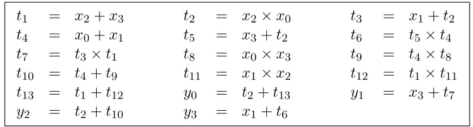
Boyar and Peralta [1] used this heuristic to find a circuit with only 5 AND gates and 11 XOR gates, but depth 9. In terms of size, this was a significant improvement over previous constructions. None of these constructions, however, was concerned with depth. To minimize depth, we used a different parametrization of these techniques and found a circuit with depth 4 and size 17. The straight-line program for the circuit is in Figure 1 (arithmetic is overGF(2)).
t1 = x2+x3 t2 = x2×x0 t3 = x1+t2
t4 = x0+x1 t5 = x3+t2 t6 = t5×t4
t7 = t3×t1 t8 = x0×x3 t9 = t4×t8
t10 = t4+t9 t11 = x1×x2 t12 = t1×t11
t13 = t1+t12 y0 = t2+t13 y1 = x3+t7
y2 = t2+t10 y3 = x1+t6
Figure 1: Inversion in GF(24). Input is (x0, x1, x2, x3) and output is (y0, y1, y2, y3).
4
A greedy heuristic for linear components
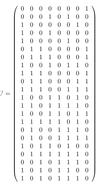
The largest linear components in our circuit are the top linear and bottom linear compo-nents. These components contain more than the linear operations defined explicity in the definition of the AES S-box and the matrices to do the basis changes. This is because they include some of the finite field inversion operations. The top linear component is defined by the matrix U, a 22×8 matrix (Figure 2). One can compute all 22 of the required outputs with only 23 XOR gates, and 23 are necessary [1, 5, 4]. But these results do not attempt to minimize depth (the depth is 7). Since there are only 8 columns in this matrix, each of the 22 outputs could clearly be calculated independently using depth at most 3, simply by using a balanced binary tree with the inputs as leaves. The challenge is to achieve the low depth without increasing the number of XOR gates drastically. The algorithm below does this. (Note that although the linear transformation at the top of Nogami et.al.’s circuit only has depth 2, they have XOR gates at depth 3, so their top linear component also has depth at least 3.)
The bottom linear component is defined by the matrix B, an 8×18 matrix (Figure 3). The row with the largest Hamming weight (number of ones = number of variables added together) has 12 ones, so depth at most 4 is possible for this component.
U =
0 0 0 0 0 0 0 1 0 0 0 1 0 1 0 0 1 0 0 0 0 0 1 0 1 0 0 1 0 0 0 0 1 0 0 0 0 1 0 0 0 1 1 0 0 0 0 1 0 1 1 1 0 0 0 1 1 0 0 1 0 1 1 0 1 1 1 0 0 0 0 1 0 1 1 0 0 0 1 1 1 1 1 0 0 1 1 1 1 0 0 1 1 0 1 0 1 1 0 1 1 1 1 0 1 0 0 1 1 0 1 1 1 1 1 1 1 0 1 0 0 1 0 0 1 1 1 0 0 1 0 0 1 1 1 1 1 0 1 1 0 1 0 0 0 1 1 1 1 1 1 0 0 0 1 0 1 1 1 0 1 0 1 0 1 1 0 0 1 0 1 0 1 1 1 0
Figure 2: The top linear transformationU.
B =
0 0 0 1 1 0 1 1 0 1 1 0 0 0 0 1 1 0 0 0 0 0 1 1 0 1 1 0 0 0 1 1 0 1 1 0 1 0 1 1 0 1 0 0 0 0 0 0 1 1 0 1 1 0 1 1 0 1 1 0 0 0 0 1 1 0 0 0 0 1 1 0 0 1 1 0 1 1 0 0 0 1 1 0 0 0 0 1 1 0 1 0 1 1 1 0 0 1 1 0 1 1 1 0 1 1 1 0 1 1 0 0 0 0 1 1 0 1 1 0 0 0 0 1 1 0 1 0 1 0 0 0 1 0 1 0 0 0 1 0 1 1 0 1
of variables. Note that in [1], the variable y11 is computed as y20 ⊕y9. Since y20 =
x0⊕x1⊕x3⊕x4⊕x5⊕x6 and y9 =x0⊕x3, the result isy11=x1⊕x4⊕x5⊕x6; the x0
and x3 are cancelled.
When attempting to find small, low-depth circuits for a linear component, one expects that cancellation of variables will be of limited help, since it would often require that something with a large Hamming weight has already been computed, before adding one to the depth at the gate where the cancellation occurs. Thus, it seems reasonable to start with a technique which does not allow cancellation, and then try to add cancellation afterwards where it helps.
We modify Paar’s technique [11], a greedy approach which produces cancellation-free programs. Paar’s technique keeps a list of variables computed, which is initially only the inputs. Then it repeatedly determines which two variables, XORed together, occur in most outputs. One such pair is selected and XORed together. This result is added as a new variable which appears in all outputs where both variables previously appeared. This is repeated until everything has been computed. Paar’s technique is implemented by starting with the initial matrix and adding columns corresponding to the new variables which are added. When a new column is added, this corresponds to adding two variables, u and v. In all rows in the matrix which currently have a one in both of the columns corresponding tou and v, those two ones are changed to zeros, and a one is placed in the corresponding row of the new column. All other values in the new column are set to zero.
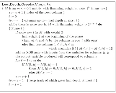
The Low Depth Greedy algorithm maintains the greedy approach of Paar’s technique, but only allows this greediness as long as it does not increase the circuit’s depth unnecessar-ily. Assume thatkis the depth we are aiming for, i.e. k=dlog2(w)e, wherewis the largest Hamming weight of any row. The Low Depth Greedy algorithm haskphases, starting with 0. At the beginning of a new phase, we check if any row has Hamming weight two. Since there must be an additional gate to produce that output, we produce it at the beginning of the phase so that it affects all counting in the current phase. During phasei≥0, no row in the current matrix has Hamming weight more than 2k−i and only inputs or gates already produced at depthior less are considered as possible inputs to gates in phasei. Thus, the depth of gates in phase i is at most i+ 1. When choosing two possible inputs for gates, one chooses a pair which occurs most frequently in the current rows, with the restriction, of course, that both inputs are at level ior less. Pseudo-code for this algorithm is given in Figure 4.
This algorithm produces a minimum depth (optimal depth) circuit.
Theorem 1 When given an m×n 0-1 matrix, M, with maximum Hamming weight at
most 2k in any row, Algorithm Low Depth Greedy, produces a correct, depth-k circuit for computing the linear component defined by the matrix. The running time is O(mt3), where
t is the final number of columns and is at most mn+n−m.
Low Depth Greedy(M, m, n, k):
{ M is anm×n0-1 matrix with Hamming weight at most 2k in any row}
s:=n+ 1{ index of the next column}
i:= 0
ip:=n { columns up tonhad depth at most i}
whilethere is some row in M with Hamming weight>2k−i−1 do {Phase i}
ifsome row `inM with weight 2
had weight 2 at the beginning of the phase
then letj1 andj2 be the columns in row` with ones
else find two columns 1≤j1, j2 ≤ip
which maximize|{`|M[`, j1] =M[`, j2] = 1}|
add an XOR gate with inputs from the variables for columns j1, j2
the output variable produced will correspond to columns
for`= 1 to mdo
if M[`, j1] =M[`, j2] = 1
thenM[`, j1] := 0;M[`, j2] := 0;M[`, s] := 1
elseM[`, s] := 0
s:=s+ 1
ip:=s−1 { keep track of which gates had depth at mosti }
i:=i+ 1
Figure 4: Algorithm for creating a minimum depth circuit for linear components
i+ 1, since combining the at most 2k−i ones any row by pairs will reduce the number of ones to at most half as many, at most 2k−i−1.
For each XOR gate added, the algorithm checks every pair of columns between 1 and
ip < s, where s is the new column being added. For each of these pairs of columns, one checks for each row if both entries corresponding to these columns are one and then does some updating. The number of rows is n, so the total running time isO(nt3). Since there are at mostnones in every row, each row will be computed using at mostn−1 XORs, and all m rows will be computed with at most m(n−1) XORs. There are n columns initially,
so in all t≤mn+n−m. 2
Another possibility for an algorithm to produce optimal depth circuits for linear compo-nents would have been to finish with all pairs of inputs before continuing to pairs involving gates at depth one, and then to finish with all pairs at depth one (or involving the possibly one remaining input which has not been paired), etc. However, the method chosen here allows more flexibility in choosing gates, thus allowing more possibilities to create gates which can be used more than once.
by calculating some outputs of the top linear component at lower depth than the depth indicated by the matrix row with largest Hamming weight, if these “outputs” are on the critical path.
It is easy to determine which outputs of the top linear component could be allowed to be at a larger depth or should be at a lower depth if possible, using a program which calculates the depth and height of every gate. If all of the outputs of the top linear component which have depth and height values adding up to exactly the total depth of the circuit are such that they could have been calculated at lower depth than their current depth, then one can probably reduce the depth of the circuit. On the other hand, when these values add up to less than the total depth of the circuit, there is someslack at that gate. For XOR gates at depth 3 (in an AES S-box circuit) which have slack, one can check if they are the sum of any two of the other outputs of the top-linear part. If they are, these other outputs were computed at depth 3, so adding them together only gives depth 4, which is acceptable when the output was originally created at a gate with slack. Note that cancellation of variables should be allowed here.
The Low Depth Greedy algorithm can be modified to take advantage of slackness. In this case, an extra array Factor is initialized for each input to the linear transformation. Rows with no slack are given the value 1, and rows that could be at j levels further down than the minimum are given the value 2j in Factor. Then, when checking if one should proceed to the next phase, rather than check if all rows have Hamming weight at most 2k−i for phasei, one checks if its Hamming weight divided by its value inFactoris at most 2k−i. This allows the possibility of choosing inputs required for these outputs at a larger depth. These techniques were not actually necessary to produce the circuits found.
5
Reducing depth in linear components
There are straight-forward techniques for reducing depth in linear components via local replacement. Consider any gate in such a component. The output produced there is the XOR of several values (either inputs or outputs from other gates). These values can be XORed in any order to get this result. Thus, for example, suppose g = g1⊕g2, g1 is at
depthd1 andg1 =g3⊕g4,g2 is at depthd2, andg3 is at depthd3. Ifd2 andd3 are at depth
at most d1−2, then calculating h1 = g2 ⊕g3 and h2 = h1⊕g4 results in h1 computing
the same result as g, but at depth one lower. If the result computed at g1 was not used
anywhere else in the circuit, then this does not increase the total number of gates. However, ifg1 is used elsewhere, it would still need to be computed, and the number of gates would
increase by one.
6
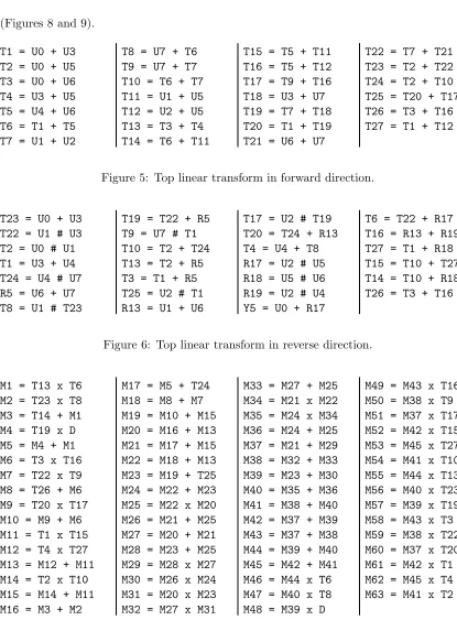
The circuits
(Figures 8 and 9).
T1 = U0 + U3 T2 = U0 + U5 T3 = U0 + U6 T4 = U3 + U5 T5 = U4 + U6 T6 = T1 + T5 T7 = U1 + U2
T8 = U7 + T6 T9 = U7 + T7 T10 = T6 + T7 T11 = U1 + U5 T12 = U2 + U5 T13 = T3 + T4 T14 = T6 + T11
T15 = T5 + T11 T16 = T5 + T12 T17 = T9 + T16 T18 = U3 + U7 T19 = T7 + T18 T20 = T1 + T19 T21 = U6 + U7
T22 = T7 + T21 T23 = T2 + T22 T24 = T2 + T10 T25 = T20 + T17 T26 = T3 + T16 T27 = T1 + T12
Figure 5: Top linear transform in forward direction.
T23 = U0 + U3 T22 = U1 # U3 T2 = U0 # U1 T1 = U3 + U4 T24 = U4 # U7 R5 = U6 + U7 T8 = U1 # T23
T19 = T22 + R5 T9 = U7 # T1 T10 = T2 + T24 T13 = T2 + R5 T3 = T1 + R5 T25 = U2 # T1 R13 = U1 + U6
T17 = U2 # T19 T20 = T24 + R13 T4 = U4 + T8 R17 = U2 # U5 R18 = U5 # U6 R19 = U2 # U4 Y5 = U0 + R17
T6 = T22 + R17 T16 = R13 + R19 T27 = T1 + R18 T15 = T10 + T27 T14 = T10 + R18 T26 = T3 + T16
Figure 6: Top linear transform in reverse direction.
M1 = T13 x T6 M2 = T23 x T8 M3 = T14 + M1 M4 = T19 x D M5 = M4 + M1 M6 = T3 x T16 M7 = T22 x T9 M8 = T26 + M6 M9 = T20 x T17 M10 = M9 + M6 M11 = T1 x T15 M12 = T4 x T27 M13 = M12 + M11 M14 = T2 x T10 M15 = M14 + M11 M16 = M3 + M2
M17 = M5 + T24 M18 = M8 + M7 M19 = M10 + M15 M20 = M16 + M13 M21 = M17 + M15 M22 = M18 + M13 M23 = M19 + T25 M24 = M22 + M23 M25 = M22 x M20 M26 = M21 + M25 M27 = M20 + M21 M28 = M23 + M25 M29 = M28 x M27 M30 = M26 x M24 M31 = M20 x M23 M32 = M27 x M31
M33 = M27 + M25 M34 = M21 x M22 M35 = M24 x M34 M36 = M24 + M25 M37 = M21 + M29 M38 = M32 + M33 M39 = M23 + M30 M40 = M35 + M36 M41 = M38 + M40 M42 = M37 + M39 M43 = M37 + M38 M44 = M39 + M40 M45 = M42 + M41 M46 = M44 x T6 M47 = M40 x T8 M48 = M39 x D
M49 = M43 x T16 M50 = M38 x T9 M51 = M37 x T17 M52 = M42 x T15 M53 = M45 x T27 M54 = M41 x T10 M55 = M44 x T13 M56 = M40 x T23 M57 = M39 x T19 M58 = M43 x T3 M59 = M38 x T22 M60 = M37 x T20 M61 = M42 x T1 M62 = M45 x T4 M63 = M41 x T2
Figure 7: Shared part of AES S-box circuit (D=U7 in the forward direction and D=Y5 in the reverse direction).
L0 = M61 + M62 L1 = M50 + M56 L2 = M46 + M48 L3 = M47 + M55 L4 = M54 + M58 L5 = M49 + M61 L6 = M62 + L5 L7 = M46 + L3 L8 = M51 + M59 L9 = M52 + M53
L10 = M53 + L4 L11 = M60 + L2 L12 = M48 + M51 L13 = M50 + L0 L14 = M52 + M61 L15 = M55 + L1 L16 = M56 + L0 L17 = M57 + L1 L18 = M58 + L8 L19 = M63 + L4
L20 = L0 + L1 L21 = L1 + L7 L22 = L3 + L12 L23 = L18 + L2 L24 = L15 + L9 L25 = L6 + L10 L26 = L7 + L9 L27 = L8 + L10 L28 = L11 + L14 L29 = L11 + L17
S0 = L6 + L24 S1 = L16 # L26 S2 = L19 # L28 S3 = L6 + L21 S4 = L20 + L22 S5 = L25 + L29 S6 = L13 # L27 S7 = L6 # L23
Figure 8: Bottom linear transform in forward direction. Outputs are S0. . . S7.
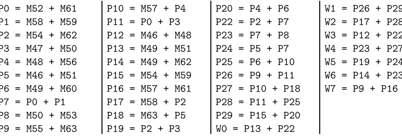
P0 = M52 + M61 P1 = M58 + M59 P2 = M54 + M62 P3 = M47 + M50 P4 = M48 + M56 P5 = M46 + M51 P6 = M49 + M60 P7 = P0 + P1 P8 = M50 + M53 P9 = M55 + M63
P10 = M57 + P4 P11 = P0 + P3 P12 = M46 + M48 P13 = M49 + M51 P14 = M49 + M62 P15 = M54 + M59 P16 = M57 + M61 P17 = M58 + P2 P18 = M63 + P5 P19 = P2 + P3
P20 = P4 + P6 P22 = P2 + P7 P23 = P7 + P8 P24 = P5 + P7 P25 = P6 + P10 P26 = P9 + P11 P27 = P10 + P18 P28 = P11 + P25 P29 = P15 + P20 W0 = P13 + P22
W1 = P26 + P29 W2 = P17 + P28 W3 = P12 + P22 W4 = P23 + P27 W5 = P19 + P24 W6 = P14 + P23 W7 = P9 + P16
Figure 9: Bottom linear transform in reverse direction. Outputs are W0. . . W7.
long as the topology derived from the tower-of-fields method is maintained, we conjecture that it is unlikely that the size of the circuits can be significantly reduced without increasing the depth. We also conjecture that it is unlikely that the depth can be reduced without significantly increasing size. Of course, if the logical base is expanded, we may be able to do better. For example, if NAND gates are used in the circuit for inversion inGF(24), it is not hard to reduce the number of gates by two without increasing the depth. Since there are only 256 possible inputs, we verified the circuits fully against the specifications in [9].
References
[1] J. Boyar and R. Peralta. A new combinational logic minimization technique with applications to cryptology. In P. Festa, editor,SEA, volume 6049 ofLecture Notes in Computer Science, pages 178–189. Springer, 2010.
[2] J. Boyar, R. Peralta, and D. Pochuev. On the multiplicative complexity of Boolean functions over the basis (∧,⊕,1). Theoretical Computer Science, 235:43–57, 2000.
[4] C. Fuhs and P. Schneider-Kamp. Optimizing the AES S-Box using SAT. InProceedings of the 8th International Workshop on the Implementation of Logics, 2010.
[5] C. Fuhs and P. Schneider-Kamp. Synthesizing shortest linear straight-line programs over GF(2) using SAT. In O. Strichman and S. Szeider, editors,SAT, volume 6175 of
Lecture Notes in Computer Science, pages 71–84. Springer, 2010.
[6] T. Itoh and S. Tsujii. A fast algorithm for computing multiplicative inverses inGF(2m) using normal bases. Inf. Comput., 78(3):171–177, 1988.
[7] O. B. Lupanov. A method of circuit synthesis. Izvestia V.U.Z. Radiofizika, 1:120–140, 1958.
[8] S. Morioka and A. Satoh. An optimized S-Box circuit architecture for low power AES design. InRevised Papers from the 4th International Workshop on Cryptographic Hardware and Embedded Systems, pages 172–186, London, UK, 2003. Springer-Verlag.
[9] NIST. Advanced Encryption Standard (AES) (FIPS PUB 197). National Institute of Standards and Technology, November 2001.
[10] Y. Nogami, K. Nekado, T. Toyota, N. Hongo, and Y. Morikawa. Mixed bases for effi-cient inversion inf(((22)2)2) and conversion matrices of subbytes of AES. In S.
Man-gard and F.-X. Standaert, editors,CHES, volume 6225 of Lecture Notes in Computer Science, pages 234–247. Springer, 2010.
[11] C. Paar. Optimized arithmetic for Reed-Solomon encoders. In IEEE International Symposium on Information Theory, page 250, 1997.