Bandwidth Optimisation for Semiconductor Junction Circulators
Ghassan N. Jawad* and Robin Sloan
Abstract—This paper presents for the first time a systematic algorithm to optimise the bandwidth for a semiconductor junction circulator with minimum magnetic bias requirements. The behaviour of the gyroelectric parameters was studied to describe the optimum biasing magnetic field for millimetre wave operation with maximum bandwidth. Perfect circulation conditions derived using a Green’s function approach were analysed to determine the optimum radius and coupling half-angle for the semiconductor disk forming the circulator. Previously measured data for InSb at 77 K were used to find design parameters for optimum bandwidth of circulation at millimetre wave frequencies. The performance of the design was verified using a full-wave electromagnetic simulation package, where up to 90% 10 dB bandwidth centred at 200 GHz was achieved with magnetic biasing as low as 0.214 T.
1. INTRODUCTION
Circulators are passive microwave devices that are mainly used as duplexers for conveying signals to receivers or transmitters as needed using one antenna in the system front end [1]. Therefore, they have many uses in radar and communication systems.
Commercial circulators are designed and fabricated using gyromagnetic materials, primarily ferrites. At microwave frequencies, circulators employing ferrites give high differential isolation, low insertion loss, and stable performance with low biasing magnetisation requirements [2]. However, at higher frequencies (such as mm-wave, and THz frequencies), ferrite circulators require very high magnetic bias to achieve broadband circulation [3]. Some ferrite circulator designs have been proposed to overcome the high biasing requirements [4, 5]. However, only narrowband circulation was achieved for the millimetre-wave frequency range.
Modern developments in microwave circuit technology and the emergence of higher frequency ranges increase the need for circulators with compact size and high frequency capabilities [6–8]. Therefore, it is essential to introduce circulators that can provide broadband performance at high frequencies, and, at the same time, compact enough to be included in Microwave Monolithic Integrated Circuits (MMICs). Semiconductor Junction Circulators (SJC’s) were first introduced by Davis and Sloan in 1993 [9], where the gyroelectric properties of magnetised semiconductors were utilised to design non-reciprocal devices working in the mm-wave frequency range and can be integrated with microwave circuits.
The Drude-Zener model of magnetised plasma [10] was used to introduce a tensor permittivity, which is applied to the circulator’s electromagnetic analysis. As with ferrite stripline junction circulators, Bosma’s Green’s function approach [11] was used to determine electromagnetic field distribution on the circulator, and calculate scattering parameters.
According to the Green’s function circulator analysis method, perfect circulation conditions were derived in [12] as roots for the electromagnetic equations in the case of perfect circulation (0 dB insertion loss,−∞dB isolation). Similar equations were solved for a SJC and used to find the required parameters and dimensions to achieve perfect circulation at a certain frequency [9].
Received 14 December 2014, Accepted 2 February 2015, Scheduled 28 February 2015 * Corresponding author: Ghassan Nihad Jawad ([email protected]).
In [13], it was shown that careful choice of magnetic bias and coupling parameters for the circulator would enable it to track perfect circulation conditions over wide range of frequencies. To improve the bandwidth even further, operation of the circulator was extended to frequency ranges where the effective permittivity of the magnetised semiconductor (eff) is negative. Theoretical broadband designs reported
in [2, 13] were validated by calculating their scattering parameters depending on real measured data of the semiconductor in use.
However, applying previously reported broadband SJC design parameters to a full wave electromagnetic simulator using the recently added gyroelectric materials simulation features did not yield the same expected performance. Instead, further tuning for some parameters was required to approach the desired results. In addition, operating in the negative eff region did not produce the
same expected circulation performance, which is attributed to the evanescent nature of resonant modes in that case.
The systematic approach presented here produces design parameters that assure tracking perfect circulation conditions for the widest possible frequency range with minimum magnetic bias requirement. Small magnetic bias implies smaller physical size for the circulator resulted from minimising the required permanent magnet. Only frequency regions with positive effective permittivity were included to eliminate the undesired behaviour of evanescent modes. Resulting optimum design parameters for an InSb at 77 K were used to validate the broadband operation using a full wave electromagnetic simulation package.
2. THEORETICAL BACKGROUND
Gyroelectric properties arise from magnetising a piece of semiconductor with a steady magnetic field, which yields a tensor permittivity. The tensor permittivity of a semiconductor magnetised inzdirection is expressed as [9]:
[] =
ε −jκ 0
jκ ε 0
0 0 ζ
(1)
where:
ε = r
⎡
⎣1− ω
2
p(ω−jυc)
ω
(ω−jυc)2−ω2c
⎤
⎦ (2)
κ = r
⎡
⎣ ω2pωc
ω
(ω−jυc)2−ωc2
⎤
⎦ (3)
ζ = r
1− ω
2
p
ω(ω−jνc)
(4)
r is the dielectric constant of the semiconductor, νc the effective electron collision frequency (in s−1), and ωp andωc are the plasma and cyclotron radian frequencies, respectively.
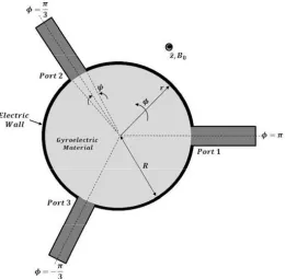
Figure 1 shows a diagram for a SJC, it is assumed that no field change occurs along the axis of the gyroelectric disk (∂z∂ = 0). In addition, only TE modes (Eφ, Er, and Hz) are considered for analysis since they are responsible for exciting gyroelectric behaviour. Applying the permittivity tensor in (1) to Maxwell’s equations results in the Helmholtz equation [13]:
∂2Hz
∂r2 +
1 r ∂Hz ∂r + 1 r2 ∂2Hz
∂φ2 +k 2
effHz = 0 (5)
wherekeff is the effective wavenumber, and is expressed by:
Figure 1. A diagram of the Semiconductor Junction Circulator (SJC).
where μ0 and ε0 are the permeability and permittivity of vacuum, respectively. eff is the effective
permittivity of the magnetised semiconductor, and can be described in terms of diagonal and off-diagonal elements of the permittivity tensor as:
eff = ε
2−κ2
(7)
Solution of the Helmholtz equation in (5) for real keff(eff ≥0) and finite magnetic field at the centre of the disk is given by [9]:
Hz,n(r, φ) =anJn(keffr)ejnφ (8)
where an is a constant, and Jn is the nth order Bessel function of the first kind. Using Maxwell equations, Electric field components (Eφ and Er) can be found in terms of partial derivatives of Hz,n in (8).
According to Fig. 1, the electric wall is assumed to encircle the gyroelectric material from all sides except for the three even spaced 2ψ suspended port locations. It is also assumed that the top and bottom of the gyroelectric disk are bounded in magnetic walls. Considering the tangential electric field (Eφ) at each port to be constant across its width, the axial magnetic field (Hz) can be related toEφ at all ports by virtue of a Green’s function [9]:
Hz,n(r, φ) =
π
−π
Gr, φ;r, φEφ
R, φdφ (9)
The average magnetic field across theith port is defined by [9]:
Hz,n= 1 2ψ
θ−ψ
θ+ψ
Hz(φ)dφ (10)
whereiis the port’s index, andθ isπ, π3, and −π3 for ports 1, 2, and 3, respectively.
equating that to the expression in (5). Comparing the result to (9) would yield the following expression for the Green’s function:
Gφ;φ= −j 2πZeff
∞
n=−∞
Jn(X)ejn(φ−φ )
Jn(X)−κεXnJn(X)
(11)
whereX =keffR. It is assumed that the tangential electric field (Eφ) is constant across the three ports. Hence, when substituting (10) into (9), only the Green’s function will be integrated twice. Scattering parameters can be found by using the integrated Green’s function to relate electromagnetic fields at circulator’s ports.
In order to have perfect circulation, one of the transmission parameters between ports (S12, orS13)
should be zero. Equating one of these two quantities to zero results in two equations that can be solved for the main design parameters: gyroelectric ratio (κε), surrounding-to-effective impedance ratio ( Zd
Zeff),
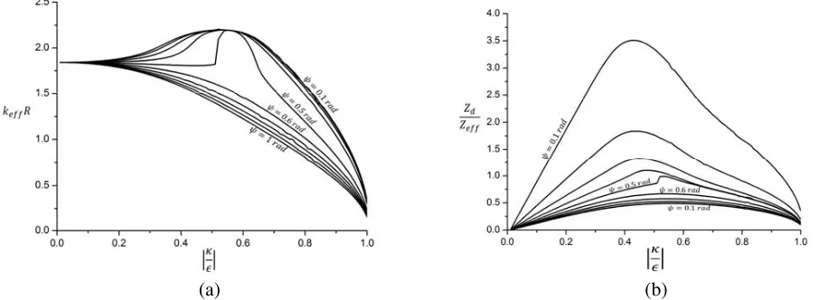
radius (R), and the coupling half angle (ψ), they are called the perfect circulation conditions [13]. Figure 2 shows the perfect circulation conditions resulted from solving the first and second circulation equations for different values of coupling half angles (ψ’s).
(a) (b)
Figure 2. Solution of the perfect circulation equations: (a) First equation, and (b) second equation.
Designing a circulator to work at a specific frequency is normally started by finding the surrounding-to-effective impedances ratio ( Zd
Zeff) and the gyroelectric ratio (
κ
ε) at that frequency. Applying these two values to the second perfect circulation conditions in Fig. 2(b) will define a point on the plot, the coupling half angle of the circulator (ψ) is chosen as the one associated with the closest line to that point.
The normalised wavenumber (keffR) can then be found by applying the value of κε to the chosenψ
line in the first circulation condition in Fig. 2(a). The circulator’s radius (R) can be deduced from
keffR since the effective wavenumber keff can be directly found at the design frequency from the
semiconductor’s properties using (6) and (7).
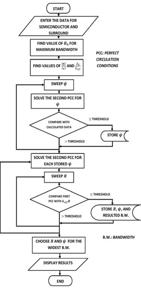
3. THE PROPOSED ALGORITHM
Previous attempts to design a broadband SJC relied on tracking both perfect circulation conditions for the widest possible bandwidth by carefully choosing the circulator’s design parameters (ψ, R,B0, and d), wheredis the permittivity of the surrounding material [2, 13]. Nevertheless, that procedure lacked accuracy, and its results did not meet expectation when simulating the reported designs.
Tracking perfect circulation conditions is possible when Zd
Zeff changes with
κ
ε for the magnetised semiconductor in the same way as in the second circulation condition shown in Fig. 2(b).
It can be shown that in general, Zd
Zeff decreases when the frequency increases for positive eff. On
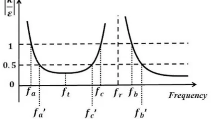
the other hand, for a lossless semiconductor (υc = 0), |κε|changes with frequency as shown in Fig. 3.
Figure 3. The change of|κε|with frequency for a magnetized semiconductor.
Its values start from∞ at f = 0, and decreases until crossing 1 and 0.5 atfa and fa, respectively. Atft,|κε|starts to increase to cross 0.5 and 1 again atfc andfc (the cyclotron frequency), respectively. A discontinuity occurs at the extraordinary wave resonance frequency (fr), where the value of|κε|goes to ∞ and decreases afterwards crossing 1 and 0.5 at fb andfb, respectively.
Regions of operation for a SJC are usually defined to be either fa < f < fc, or f > fb. This is because these are the regions whereeff is positive, and hence, the effective wavenumber is real. At the
same time, frequencies near fr are avoided because they are associated with high loss (when υc = 0). From above, it can be noticed that when d|κε|
df is negative (the value is decreasing with frequency), the tendency of Zd
Zeff −
κ
ε curve is the same as that in the second perfect circulation condition curves in Fig. 2(b) for |κε|>0.5. In addition, when d|κε|
df is positive (value is increasing), ZZeffd −
κ
ε curve has the same tendency of the curves in Fig. 2(b) for|κε|<0.5.
Hence, tracking the second perfect circulation lines is possible for three bands: fa < f < fa,
ft< f < fc, andfb < f < fb. The closeness of the latter band to fr makes it less desirable for design because of the high loss. Moreover, a high bias field is required to make the second band include more frequencies. The widest band that can be achieved with minimum magnetic biasing is the first one of negative|κε|slope, which will be used in this algorithm.
In order to maximise the bandwidth, it was shown thatB0 has to be chosen such that gyroelectric
ratio atft should be equal to 0.5, i.e., ftand fa merge. This happens when ω2c = 0.278ωp2, as shown in Appendix A.
After finding the biasing field (B0) that gives the widest band fromfa tofa, values of κε,keff, and Zd
Zeff for the above range can be defined.
The second perfect circulation equation is then solved for a range of coupling half angles. For each solution, the resulting Zd
Zeff versus
κ
ε is compared to the same quantity of the device, if the distance between the two curves for certain range of κε was less than a pre-defined threshold, the range is saved as a possible tracking region, then the second perfect circulation equation is solved again for anotherψ, and so on.
is possible. The bandwidth for each one can be calculated, and the widest bandwidth along with the optimum R and ψ can then be chosen accordingly. Fig. 4 shows a flow chart for the proposed optimisation algorithm.
It should be noted that the above algorithm is used to find the optimum parameters for a specific semiconductor surrounded by a certain material with a permittivity of d. It is possible to include d in the algorithm and find its value that gives the widest range. Nevertheless, the surrounding material is identified by the microwave circuit itself, and it is not possible in practice to find a material with an exact chosen value of permittivity.
4. RESULTS AND DISCUSSION
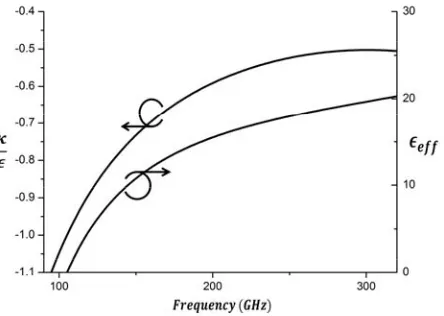
SJCs with optimum bandwidth were designed and simulated using previously measured data for InSb at 77 K [2]. Carrier concentration and electron mobility were 1.7×10²⁰m−3and 54 m2V−1s−1, respectively. The biasing magnetic field required to maximise the region of possible tracking (between fa and fa in Fig. 3) was found to be 0.214 T. Fig. 5 shows the behaviour of κε andeff with frequency in the frequency
range of interest. It should be noted that the ultimate bandwidth can be anticipated to be from 100 to 300 GHz (100%). However, tracking is not always possible for the whole band given the aboveB0 as
will be shown later.
Figure 5. Behaviour of κε and eff with frequency for InSb at 77 K magnetized withB0 = 0.214 T.
Different possible values for the surrounding material permittivity were used to demonstrate its effect on the overall tracking possibility.
4.1. Dielectric Constant of the Surround (d) = 2.2
This value was chosen to demonstrate the tracking potential using RT-Duroid 5880 that was used to surround the previously reported SJCs [2, 14]. Due to the low value of d in comparison to that of eff shown in Fig. 5, surrounding impedance is higher than the effective impedance for almost all the band. Hence, Zd
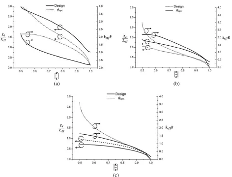
Zeff varies between about 1 and 3 for this case, as shown in Fig. 6(a).
According to the first perfect circulation graph in Fig. 2(b), the closest line is for ψ = 0.1 rad. However, by applying the algorithm to the current situation taking into account the whole band, it appeared that despite the second circulation condition having the same tendency as the resulted Zd
Zeff,
first circulation condition does not have the same tendency as keff multiplied by any value of R, as
shown in Fig. 6(a). For this reason, close tracking for both conditions is not possible for such low
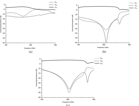
d. Although it is still possible to obtain a broadband circulation with low differential isolation and relatively high reflection. Fig. 7(a) shows a full wave simulation result of a SJC with ψ= 0.11 rad and
R= 107µm, these two parameters were a result of setting a high comparison threshold in the algorithm to allow the detection of more tracking possibilities.
4.2. Dielectric Constant of the Surround (d) = 10
The next tested value fordwas 10 (corresponding to Alumina), which is about a half of the maximum
eff in the band. ZZeffd line now lies in the middle part of the second circulation conditions graph in
(a) (b)
(c)
Figure 6. Variation of Zd
Zeff andkeffR with|
κ
ε|alongside with the perfect circulation lines for optimum
ψ for (a)d= 2.2, (b) d= 10, and (c)d= 20.
Resulted scattering parameters from simulating the above design are shown in Fig. 7(b). It is clear that the circulation is now possible with relatively high differential isolation for a wide band.
4.3. Dielectric Constant of the Surround (d) = 20
It can be concluded from the previously tested values of d that closer tracking the first circulation conditions can be achieved with higher coupling half angles since their lines have the same tendency as that of keffR of the designed device. To use higher ψ, ZZeffd should be decreased in order for the
second circulation condition to be closer to the highψ lines. This would imply the need to decrease the surrounding impedance, and hence, increase its permittivity. When choosing d= 20, which is almost the same value as the maximum eff in the band, close tracking was achieved for both circulation conditions, as shown in Fig. 6(c). It is important to remember that this tracking does not include the whole band because the difference in tendencies (especially with the first circulation condition) still exists, and the closeness was achieved for only part of the band. Nevertheless, simulating the SJC with the optimum parameters resulted into about 48% 20 dB bandwidth with about 2 dB maximum insertion loss for the whole band, as shown in Fig. 7(c).
(a) (b)
(c)
Figure 7. Simulation results for the designed circulators for (a)d= 2.2, (b)d= 10, and (c) d= 20.
(a) (b)
Figure 8. (a) Magnitude of the axial magnetic field (|Hz|) and (b) power flow on the magnetized InSb disk surrounded by a material withd= 20 at 200 GHz.
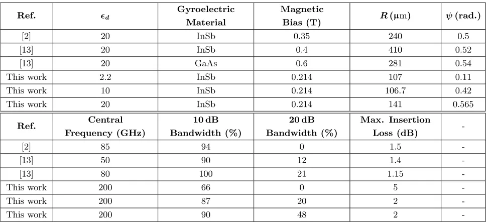
Table 1. A comparison between the outcomes of the proposed algorithm and the previously reported broadband SJC designs.
Ref. d
Gyroelectric Material
Magnetic
Bias (T) R(µm) ψ(rad.)
[2] 20 InSb 0.35 240 0.5
[13] 20 InSb 0.4 410 0.52
[13] 20 GaAs 0.6 281 0.54
This work 2.2 InSb 0.214 107 0.11
This work 10 InSb 0.214 106.7 0.42
This work 20 InSb 0.214 141 0.565
Ref. Central
Frequency (GHz)
10 dB Bandwidth (%)
20 dB Bandwidth (%)
Max. Insertion
Loss (dB)
-[2] 85 94 0 1.5
-[13] 50 90 12 1.4
-[13] 80 100 21 1.15
-This work 200 66 0 5
-This work 200 87 20 2
-This work 200 90 48 2
-5. CONCLUSION
This paper presents an algorithm to optimise the design parameters for a semiconductor junction circulator (SJC) for the first time to operate in a broadband centred by the highest possible frequency with minimum required magnetic bias. The algorithm suggests tracking the solutions of the perfect circulation equations for the widest possible frequency range.
The biasing magnetic field (B0) was calculated to maximise the frequency region where parameters
in the semiconductor and the perfect circulation conditions have the same tendency. The algorithm then uses a systematic approach to find regions where the tracking is possible for both perfect circulation curves at a certain coupling half angle ψ and circulator’s radiusR.
The algorithm was tested using realistic InSb parameters and a full wave simulation package. It was shown that the design parameters resulted from the algorithm gave the expected results for the same conditions. It was also shown from the comparison in Table 1 that the proposed algorithm can guarantee the widest possible bandwidth in the millimetre wave frequency range with minimum possible magnetic bias. Another advantage of this algorithm is the possibility of choosing the best design for a range of surround dielectric constants (d) for the same gyroelectric material, which is not provided in the previously reported broadband SJC’s.
APPENDIX A. CALCULATION OF THE OPTIMAL B0
From the definition of κ andεin (3) and (2), respectively, it can be shown that:
κ ε =
ω2pωc
ω3−ωω2
c −ωω2p
(A1)
By differentiating (A1) with respect toω and equating the result to zero, the radian frequency at which κ
ε will turn (ωc) can be found as:
ωt=
ω2
c +ω2p
3 =
ωr
√
whereωr is the extraordinary wave resonance radian frequency. The value of κε at ωt is expressed as:
κ
ε(ωt) =−
3√3 2 ω2 p ω2 c
1 +ω
2 p ω2 c −3 2 (A3)
Equating κε(ωt) to 0.5 would result into a cubic function in terms of ω
2 p
ω2c, which can be solved to
result one (realistic) root, which is equal to 0.278. Sinceωp is given by the properties of the material,
ωc can be directly found. B0 is then calculated from the cyclotron frequency using the relation [10]: ωc = e
m∗eB0 (A4)
whereeis the charge of the electron (= 1.602×10⁻¹⁹C), and m∗e is the electron’s effective mass in kg.
REFERENCES
1. Adam, J. D., L. E. Davis, G. F. Dionne, E. F. Schloemann, and S. N. Stitzer, “Ferrite devices and materials,”IEEE Transactions on Microwave Theory and Techniques, Vol. 50, No. 3, 721–737, 2002.
2. Yong, C. K., R. Sloan, and L. E. Davis, “A Ka-band indium-antimonide junction circulator,”IEEE Transactions on Microwave Theory and Techniques, Vol. 49, No. 6, 1101–1106, 2001.
3. Pardavi-Horvath, M., “Microwave applications of soft ferrites,”Journal of Magnetism and Magnetic Materials, Vol. 215, 171–183, 2000.
4. Weiss, J. A., N. G. Watson, and G. F. Dionne, “New uniaxial-ferrite millimeter-wave junction circulators,”IEEE MTT-S International Microwave Symposium Digest, 1989, 145–148, Jun. 1989. 5. Chao, L., E. Fu, V. J. Koomson, and M. N. Afsar, “Millimeter wave complementary metal-oxide-semiconductor on-chip hexagonal ferrite circulator,” Journal of Applied Physics, Vol. 115, No. 17, 17E511, 2014.
6. Cooper, K. B., R. J. Dengler, N. Llombart, B. Thomas, G. Chattopadhyay, and P. H. Siegel, “THz imaging radar for standoff personnel screening,” IEEE Transactions on Terahertz Science and Technology, Vol. 1, No. 1, 169–182, 2011.
7. Piesiewicz, R., T. Kleine-Ostmann, N. Krumbholz, D. Mittleman, M. Koch, J. Schoebel, and T. Kurner, “Short-range ultra-broadband terahertz communications: Concepts and perspectives,” IEEE Antennas and Propagation Magazine, Vol. 49, No. 6, 24–39, 2007.
8. Kallfass, I., J. Antes, T. Schneider, F. Kurz, D. Lopez-Diaz, S. Diebold, and A. Tessmann, “All active MMIC-based wireless communication at 220 GHz,”IEEE Transactions on Terahertz Science and Technology, Vol. 1, No. 2, 477–487, 2011.
9. Davis, L. E. and R. Sloan, “Semiconductor junction circulators,” IEEE MTT-S International Microwave Symposium Digest, 1993, 483–486, Jun. 1993.
10. Allis, W. P., S. J. Buchsbaum, and A. Bers, “Waves in anisotropic plasmas,”Waves in Anisotropic Plasmas, William Phelps Allis, Solomon J. Buchsbaum, and Abraham Bers, 292, ISBN 0-262-51155-X, The MIT Press, Cambridge, Massachusetts, USA, Feb. 1963.
11. Bosma, H., “On stripline Y-circulation at UHF,” IEEE Transactions on Microwave Theory and Techniques, Vol. 12, No. 1, 61–72, 1964.
12. Wu, Y. S. and F. J. Rosenbaum, “Wide-band operation of microstrip circulators,” IEEE Transactions on Microwave Theory and Techniques, Vol. 22, No. 10, 849–856, 1974.
13. Sloan, R., C. K. Yong, and L. E. Davis, “Broadband millimetric semiconductor junction circulators at 77 K,” IEEE MTT-S International Microwave Symposium Digest, 1996, Vol. 1, 109–112, Jun. 1996.