A Review of Photonic Generation of Arbitrary
Microwave Waveforms
Lam Anh Bui*
Abstract—This paper presents a tutorial on photonic techniques for arbitrary RF waveform generation, highlights some key results and reviews the recent developments in this area. It is predicted that photonic integration of the entire system as compact photonic chip will be a major research focus and holds the key role for the future developments.
1. INTRODUCTION
There are significant demands for the generations of specialized waveforms in modern applications such as communication (multiple access, high speed, multipath propagation, channel measurement) [1– 3], high resolution imaging (biology, medical tomography and spectroscopy) [4–6], electronic warfare (counter measurement and radar) [7, 8] and test and instrumentation [9]. Electronic arbitrary waveform generation (AWG) is widely used and based on high speed and high resolution Digital to Analog Converter (DAC). Although extremely versatile, electronic DAC is limited by the speed of DAC, has high timing jitter, limited Time Bandwidth Product (TBWP) and is susceptible to Electromagnetic Interference (EMI) [10, 11]. To circumvent these issues, photonic techniques for arbitrary waveform generation have been extensively investigated due to the well-known advantages associated with photonic technologies such as broad bandwidth, compatible with fibre signal distribution, reconfigurability, tunability, immunity to EMI and small size and light weight [4, 8, 11–21].
This paper provides a tutorial on photonic arbitrary waveform generations and reviews the three major approaches for AWG including i) Fourier Transform Pulse Shaping following by Frequency to Time Mapping [22–26], ii) Discrete Space to Time Mapping [27] and iii) Microwave Photonic (MWP) Filtering [1, 8, 28]. For each of these approaches, we explain the operation principle and presents selected results from the literature and highlight salient features. We also discuss what we believe to be the future developments in this area — the integration of photonic systems on a chip, review the recent developments and present some conclusions.
2. PHOTONIC APPROACH TO ARBITRARY WAVEFORM GENERATION
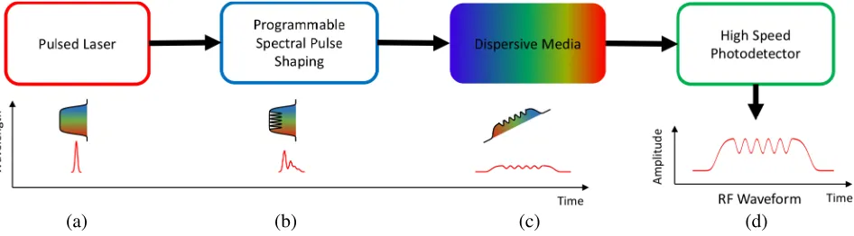
The general approach for photonic generation of high frequency and broadband RF waveforms is illustrated in Fig. 1. It consists of three main functional blocks namely optical source, optical processing and optical to electrical (O/E) conversion. The optical source generates the optical carriers that drive the other two blocks. This source could be single or multiple wavelengths and continuous or discrete in time. The optical processing block takes the optical carriers and performs operations on these signals including but not limiting to filtering, switching, mixing and mapping. Generally, there are several processing approaches; the three main approaches are i) Fourier Transform Pulse Shaping (FTPS)
Received 12 January 2017, Accepted 14 March 2017, Scheduled 15 April 2017
* Corresponding author: Lam Anh Bui ([email protected]).
Figure 1. Generic scheme for generating of an arbitrary RF waveform using a photonic technique.
following by Frequency to Time Mapping (FTM), ii) Discrete Space to Time Mapping (DSTM) and iii) Microwave Photonic Filtering (MPF). At the output of the optical processing block, the optical signals will have the desired profile/format suitable for conversion to the electrical waveforms using the optical to electrical conversion block. Detailed explanation of these approaches is given the following.
3. FOURIER TRANSFORM PULSE SHAPING AND FREQUENCY TO TIME MAPPING
As mentioned in Section 2, one of several approaches for photonic generation of arbitrary waveforms is Fourier Transform Pulse Shaping (FTPS) following by Frequency to Time Mapping (FTM) [12, 22, 23, 29]. This approach exploits the broadband feature of photonics and its inherent large Time Bandwidth Product (TBWP). Fig. 2 presents a schematic diagram illustrating the approach’s principle of operation. Optical pulse which is compact in time but very broad in spectrum is generated by a pulse laser. The spectrum of this pulse is carved out in the profile of the waveform to be generated using a programmable spectral pulse shaper and thus the approach borrows its name FTPS. After shaping the optical pulse is distorted but still localized in time. Passing this optical pulse through a dispersive media in which different spectral components experience frequency-dependent time delays resulting at the output the temporal intensity profile that resemblances the optical spectrum of the input optical pulse effectively mapping the spectral profile into the time domain. This temporal intensity profile could then be converted into the electrical domain using a high-speed photodetector [5, 11].
FTPS/FTM was pioneered by the work [5, 11, 24] and has been demonstrated as a versatile technique for arbitrary waveform generations. The paper [22] provides an excellent review of the past
(a) (b) (c) (d)
(a)
(b) (c)
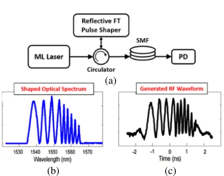
Figure 3. Arbitrary waveform generation based on Fourier Transform Pulse Shaping (FTPS) and Frequency to Time Mapping (FTM) scheme. (a) Experiment proof of concept demonstration: short optical pulses generated using mode locked laser (ML), pulse shaping based on 128-pixel linear Liquid Crystal on Silicon modulator (LCoS), Frequency to Time Mapping using ∼ 5.5 km of single mode fibre (SMF). (b) Shaped optical spectrum and (c) Generated UWB frequency linear downchirp signal that resemblances the spectral profile of (b) [12] (all figures and results are courtesy of and adapted from A. Weiner).
(a)
(b)
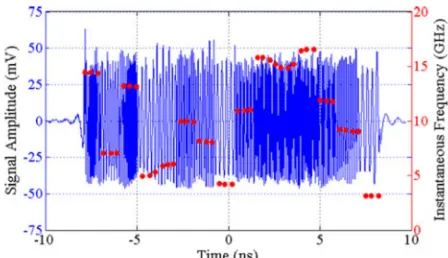
Figure 4. An improved scheme for efficient generation of arbitrary bandpass RF waveform based on Fourier Transform Pulse Shaping (FTPS) and Frequency to Time Mapping (FTM) that incorporates a delay-mismatched optical interferometer. (a) Experiment proof of concept setup: optical pulse is split into two paths, the upper path sent to FTPS to define the envelope of the generated waveform, the lower path is delayed such that its interference with the upper path forms oscillation corresponding to the center frequency of the generated RF waveform. (b) Generation of RF frequency downchirp waveform spanning 7–45 GHz with the Time Bandwidth Product (TBWP) of ∼ 589 [29] (all figures and results are courtesy of and adapted from A. Weiner).
and recent developments of this approach. A great proof of concept demonstration of the approach is present in Fig. 3 [12]. The details of the demonstrations and the results are provided in the figure caption. It is evident that the experimental setup of Fig. 3(a) is the direct implementation of the approach of Fig. 2 and the generated RF waveform of Fig. 3(c) exhibits great similarity with the shaped spectral profile of Fig. 3(b) proving the approach experimentally.
optical interferometer.
(a)
(b)
(c)
(d)
Figure 5. Waveform distortion induced during Frequency to Time Mappings. (a) Far Field Dispersion causing temporal waveform distortion. (b) Evidence of distortion due to dispersion induced frequency fading. (c) Overcoming dispersion induced distortion using Near Field Dispersion. (d) Evidence of elimination of frequency fading in the signal spectrum [23] (all figures and results are courtesy of and adapted from A. Weiner).
Figure 6. Demonstration of time aperture expansion by pseudo-noise modulation of the optical pulse train through the generation of a microwave Costas sequence — Time domain measurement of the W-band Costas sequence with a 10 GHz center frequency and a 1 GHz frequency step [29] (all figures and results are courtesy of and adapted from A. Weiner).
It has been previously mentioned that the dispersive delay is employed to map the spectral profile into the temporal intensity profile. To achieve this, sufficient dispersion in the order of the square of the optical pulse duration — also known as far field dispersion condition — must be satisfied [23]. Using a large dispersion can however limit the bandwidth and the upper frequency content of the generated waveforms due to the dispersion induced frequency fading effect [23] which is observed in the measurements of Figs. 5(a) and 5(b). To overcome this limitation, a near field dispersion condition has been proposed and demonstrated [23]. In this later scheme, a significantly smaller dispersion than that would be required for far field condition is used resulting in the output temporal intensity depending on both the amplitude and the phase of the spectral profile making the process of FTM more complicated. Fortunately, dispersion is a fully defined process and therefore the FTPS could be programmed to pre-distort the spectral profile to compensate for this phase dependency [23]. Figs. 5(c) and 5(d) presents the results obtained using near field dispersion which overcomes the frequency fading problem of Figs. 5(a) and 5(b).
The approach of Fig. 2 requires the optical carriers in the form of short optical pulse which is repetitive in nature and thus the generated waveforms are limited by the time gap between the two adjacent pulses limiting their practical uses. Several works have been done to overcome this constraint including pulse by pulse shaping [25] and pseudo-noise pulse switching [30]. Fig. 6 presents a practical demonstration of a 15-times aperture expansion using a pseudo-noise switching to generate a W-band Costas sequence of length 15 [29]. With this technique, it is possible to extend the time limited waveform to an almost arbitrary time length which is necessary for high resolution radar and ranging applications.
4. DIRECT SPACE TO TIME MAPPING
(a) (b) (c)
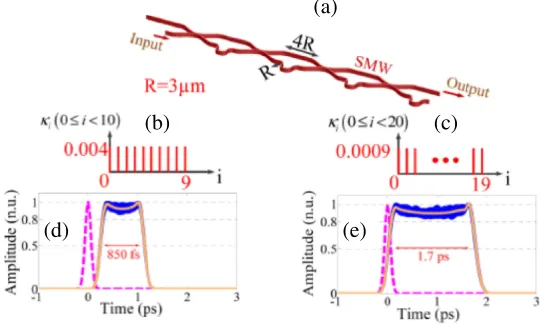
Figure 7. Arbitrary waveform generation based on the Discrete Space to Time Mapping (DSTM) of short-time optical pulses. (a) Operation principle and the device schematic consisting of n cascaded stages of weak coupling and time delay to generate temporal waveform havingndiscrete amplitude levels with each level lasting a specific delayed duration. (b) Realising and controling of coupling coefficient using a waveguide coupler. (c) Realising and precise controling of the time delay and phase shift using differential waveguide delay lines [27] (all figures and results are courtesy of and adapted from J. Azana).
(a)
(b) (c)
(d) (e)
Figure 8. Generation of flattop waveforms of different temporal durations using the DSTM scheme of Fig. 7. (a) Simulated output waveform of 850 fs width for a device with 10-stages using an input optical Gaussian pulse of 150 fs duration. (b) Simulated output waveform of 1.7 ps pulse-width for a similar device with 20-stages using a 150 fs Gaussian input pulse [27] (all figures and results are courtesy of and adapted from J. Azana).
of Fig. 7(a) [27]. Each of these impulses is weighted by the respective coupling coefficient and delayed by the accumulated time between the input and the considered stage itself [27]. By tailoring these stages (coupling coefficient and delay), any waveform profile can be generated as illustrated by the inset temporal waveform (red) of Fig. 7(a). Figs. 7(b) and 7(c) propose a possible realization and control of the coupling coefficient (amplitude coding) and phase plus delay (phase coding) using a waveguide coupler and a waveguide length-difference respectively. It is also possible to incorporate electrodes into these waveguiding elements to allow tuning — enabling reconfiguration of the waveform.
(a) (b)
Figure 9. Generation of a complex 8-symbol 16 QAM signal at 24 GSymbols/s from a Gaussian optical pulse of 17 ps width using a 24-stages device. (a) 24 complex coupling coefficients. (b) Generated complex waveform [27] (all figures and results are courtesy of and adapted from J. Azana).
generation of the targeted waveform in Fig. 9(b) demonstrates the versatility and the effectiveness of the technique. Comparing the results of Fig. 8 and Fig. 9, it is evident that this technique can generate waveforms spanning a wide temporal duration ranging from sub-picosecond to sub-nanosecond regime. Furthermore, the small coupling values used to satisfy the weak coupling condition results in a rather low amplitude for the device transfer function, however it has been shown that a moderate energy efficiency approaching 50% could be achieved by using many design stages.
5. MICROWAVE PHOTONIC FILTERING
This approach to generate arbitrary waveform leverages on the wealth of developments around broadband and reconfigurable microwave photonic filters [8, 9, 14, 15]. The overall principle of this approach is illustrated in Fig. 10 in both time and frequency domains. The core guiding philosophy is to design a microwave photonic filter such that its impulse response is the waveform profile of interest. Spectrally, this could be understood as filtering the broad spectrum of a narrow pulse to obtain the spectrum profile which is the Fourier transform of the temporal waveform of interest.
Many demonstrations of microwave photonic filters with programmable and reconfigurable capability have been reported throughout the years [8, 9, 14]. A typical microwave phonic filter consists of optical source which can be single or multiple wavelengths and discrete or continuous in time. The optical source provides the carriers in which a short electrical pulse is modulated onto. The modulated optical signal is then processed in a photonic system which consists of several elements including couplers, Fibre Bragg Gratings (FBG), filters, attenuators, modulators, delay lines, amplifiers, and mixers before optical to electrical conversion using high speed photodetectors to obtain the desired RF waveforms. Utilization of these filters to generate arbitrary waveforms have also been demonstrated [1, 8, 9, 14, 28]. In the following we selectively presents results that highlight several salient features of this approach.
Figure 11 presents the generation of Ultra-Wideband (UWB) pulses having spectrum that fits
four-taps FIR filter is generated satisfying the FCC mask requirements [1]. Given the large degree of freedom associated with the N-taps filter structure, it is possible and has been demonstrated to adapt this scheme to produce a wide range of waveforms and modulation formats including but not limited to Pulse Amplitude Modulation (PAM), On-Off Keying (OOK), Orthogonal Pulse Modulation (OPM), Pulse Position Modulation (PPM) and many more [1].
For strongly banded waveforms, it is possible to incorporate an optical delay-mismatched interferometer to generate oscillation associating with the center frequency of the generated waveform in a similar fashion used in Section 3 and specifically in Fig. 4 [28, 31]. The interferometric structure
(a) (b)
Figure 11. Generation of third order UWB pulse that satisfies the FCC mask requirement using a 4-tap transversal microwave photonic filter using an electrical pulse of approximately 50 ps temporal width. (a) Simulated (blue) and measured (black) electrical pulse. (b) FCC mask (blue) and measured spectrum (black) [1] (all figures and results are courtesy of and adapted from J. Capmany).
(a) (b)
is often employed with a balanced photodetector to remove the strong DC component from the output RF waveforms to further enhance the system efficiency [31]. Fig. 12 presents the results of generation of Multiband UWB Gaussian waveforms at 4 GHz and 7 GHz generated using an Amplified Spontaneous Emission (ASE) from an Erbium Doped Fiber Amplifier (EDFA). The delay mismatch between the two arms of the Mach-Zehnder (MZ) interferometer is adjusted to change the waveform frequency. The important feature of the results of Fig. 12 is that the DC component of the waveforms has been removed and the simplicity of frequency tuning through changing the delay mismatch. It is anticipated that with the removing of the DC component, a significant improvement of the waveform spectrum at and near DC is achieved allowing much better fitting of the waveform to the FCC mask while at the same time, the waveform still maintains at relatively high power improving the signal coverage [28].
6. PHOTONIC INTEGRATION
Having discussed the various approaches to generate arbitrary RF waveforms in the previous sections, it is now necessary to consider the realization and scaling of these approaches to meet the practical applications. Until recently most of the photonic AWGs are implemented using discrete components and they are thus limited in complexity, scalability and at the same time being bulky and expensive and often exhibit poor long term stability. It is believed that photonic integration of these systems as compact photonic chips would significantly improve their performance and enables scalability and increases complexity. It is worth noting that most if not all major elements required for these systems have been demonstrated somewhat in integrated optics form [9, 15–17, 26, 32, 33]. Some attempts to integrate the entire solution as a single chip have also been reported [16, 26]. Of particular note is the Silicon Photonic platform that has been extensively researched recently taking the advantages of the availability of the high performance and commercial grade device fabrication infrastructures of the electronic industry [34, 35]. Another platform that recently attracts significant research interest is the thin-film Lithium Niobate wafer-bonded on Silicon which is compatible with Silicon Photonics and offers efficient second order nonlinearity [36]. Furthermore, the advancements in hybrid integration also allow combining of several different and occasionally exotic platforms together enabling the creation of solutions with functionalities that are not possible in a single platform [16, 17, 26].
A further challenge for photonic integration which is often overlooked and well under-addressed is packaging. Given the number of the control and signal connections associating with an AWG system, this would be a major engineering challenge that deserves further research and development. Without proper packaging solution, the concepts continue to remain as laboratory demonstrations and have limited practical uses and commercial benefits. It is anticipated that techniques to multiplex these controls and signals must be conceived and innovated as part of the integrated solution especially during the chip design stage. With limited information on this topic available, much more and in depth developments are required. Finally, to truly reduce cost and enable highly sophisticated system on a chip, it is necessary to discover new platforms that can support many elements of a microwave photonic system including optical sources, modulators, amplifiers, mixers, filters and detectors. If this is achieved, the revolutionary power of photonics will be unleased.
7. RECENT DEVELOPMENTS
channel propagation that overcomes inter-symbol interference [46] and for rapidly reconfigurable RF filtering [38, 47]. There are also significant activities in the field of waveform generation based on microwave photonic filtering, particularly the generation of triangular wave train [48, 49]. These techniques exploit the nonlinearity characteristics of the optical modulation to generate many sideband components and manipulate them via weighting, mixing, filtering and delaying before combining them in a high-speed photodetector to construct the desired RF waveforms. The demonstrations of these approaches include phase modulation [49], dual polarisation modulation [48], single drive modulation [50] and dual drive parallel modulation [51], four wave mixing effect in SOA [52], and electro-optic-oscillator [53]. Furthermore, agile frequency hopping waveforms have also been demonstrated by master and slave continuous wave (CW) laser configuration in which the lasing wavelength of the slave laser is controlled by the injecting power of the master laser through the wavelength red shift due to antiguidance effect [54]. It is evident in the above that the interest in this field remains significantly high and it is no doubt that these developments will open new capabilities for high speed and broadband applications.
8. CONCLUSIONS
In this paper, we review several approaches for photonic generation of high frequency and broadband RF waveforms. These approaches allow generations of customized and sophisticated waveform profiles and the ability to reconfigure them rapidly and in some cases cycle by cycle. Three main approaches discussed include i) Fourier Transform Pulse Shaping following by Frequency to Time Mapping, ii) Discrete Space to Time Mapping and iii) Microwave Photonic Filtering. For each of these approaches, a brief explanation of the operation principle is provided, selected results from the literature are presented and several salient features are discussed. Technique to generate strongly banded waveforms using the delay mismatched interferometer to form oscillation associating with the center frequency of the generated waveform is described and methods to extend the time aperture to overcome the limitation due to the repetitive nature of optical pulses is described. For the frequency to time mapping, the two operation regimes namely far field and near field dispersions are defined and the explanation of how far field dispersion would limit the bandwidth and the upper frequency content of the generated waveforms and how this problem could be overcome using near field dispersion are given. We also discuss what we believe would be the holy grail of microwave photonic research and the current and the future work in arbitrary waveform generation that is the photonic integration of these systems as compactly integrated and sophisticated chips. We also discuss the promise of Silicon Photonics as a platform to achieve this goal and consider the recent interest in thin film Lithium Niobate wafer-bonded on Silicon for microwave photonics and nonlinear optical processing. The challenges associated with photonic integration especially the hybrid integration and packaging were briefly touched upon. Finally, we review the recent developments in this field which leads us to conclude that photonic integration holds the key to the advancement of this important technology that if successfully realized will unleash the revolutionary power of photonics.
REFERENCES
1. Bolea, M., J. Mora, B. Ortega, and J. Capmany, “Optical UWB pulse generator using an N tap microwave photonic filter and phase inversion adaptable to different pulse modulation formats,” Optics Express, Vol. 17, 5023–5032, 2009.
3. Pan, S. and J. Yao, “UWB-over-fiber communications: Modulation and transmission,” Journal of Lightwave Technology, Vol. 28, 2445–2455, 2010.
4. Goda, K., K. Tsia, and B. Jalali, “Serial time-encoded amplified imaging for real-time observation of fast dynamic phenomena,”Nature, Vol. 458, 1145–1149, 2009.
5. Hansen, H., “Standoff detection using millimeter and submillimeter wave spectroscopy,”Proceedings of the IEEE, Vol. 95, 1691–1704, 2007.
6. Miyakawa, M. and J. C. Bolomey, Non-invasive Thermometry of the Human Body, CRC Press, 1995.
7. Nashashibi, A. Y., K. Sarabandi, P. Frantzis, R. D. De Roo, and F. T. Ulaby, “An ultrafast wide-band millimeter-wave (MMW) polarimetric radar for remote sensing applications,” IEEE Transactions on Geoscience and Remote Sensing, Vol. 40, 1777–1786, 2002.
8. Capmany, J., J. Mora, I. Gasulla, J. Sancho, J. Lloret, and S. Sales, “Microwave photonic signal processing,” Journal of Lightwave Technology, Vol. 31, 571–586, 2013.
9. Capmany, J. and D. Novak, “Microwave photonics combines two worlds,”Nature Photonics, Vol. 1, 319–330, 2007.
10. Yu, X., K. Wang, X. Zheng, and H. Zhang, “Incoherent photonic digital-to-analogue converter based on broadband optical source,” Electronics Letters, Vol. 43, 1, 2007.
11. Han, Y. and B. Jalali, “Photonic time-stretched analog-to-digital converter: Fundamental concepts and practical considerations,”Journal of Lightwave Technology, Vol. 21, 3085, 2003.
12. Lin, I. S., J. D. McKinney, and A. M. Weiner, “Photonic synthesis of broadband microwave arbitrary waveforms applicable to ultra-wideband communication,” IEEE Microwave and Wireless Components Letters, Vol. 15, 226–228, 2005.
13. Jason, C., H. Yan, and B. Jalali, “Adaptive RF-photonic arbitrary waveform generator,” IEICE Transactions on Electronics, Vol. 86, 1226–1229, 2003.
14. Yao, J., “Photonic generation of microwave arbitrary waveforms,” Optics Communications, Vol. 284, 3723–3736, 2011.
15. Chen, L. R., “Photonic generation of chirped microwave and millimeter wave pulses based on optical spectral shaping and wavelength-to-time mapping in silicon photonics,” Optics Communications, Vol. 373, 70–81, 2016.
16. Fandi˜no, J. S., P. Mu˜noz, D. Dom´enech, and J. Capmany, “A monolithic integrated photonic microwave filter,”Nature Photonics, Vol. 11, 124–129, Oct. 23, 2016.
17. Marpaung, D., C. Roeloffzen, R. Heideman, A. Leinse, S. Sales, and J. Capmany, “Integrated microwave photonics,” Laser &Photonics Reviews, Vol. 7, 506–538, 2013.
18. Shoeiby, M., A. Mitchell, and L. Bui, “Real time all optical correlator for serialized time encoded signals,”Optics Communications, Vol. 338, 34–39, 2015.
19. Sarkhosh, N., H. Emami, L. Bui, and A. Mitchell, “Reduced cost photonic instantaneous frequency measurement system,” IEEE Photonics Technology Letters, Vol. 20, 1521–1523, 2008.
20. Emami, H., N. Sarkhosh, L. Bui, and A. Mitchell, “Amplitude independent RF instantaneous frequency measurement system using photonic Hilbert transform,”Optics Express, Vol. 16, 13707– 13712, 2008.
21. Emami, H., N. Sarkhosh, L. A. Bui, and A. Mitchell, “Wideband RF photonic in-phase and quadrature-phase generation,”Optics Letters, Vol. 33, 98–100, 2008.
22. Rashidinejad, A., Y. Li, and A. M. Weiner, “Recent advances in programmable photonic-assisted ultrabroadband radio-frequency arbitrary waveform generation,” IEEE Journal of Quantum Electronics, Vol. 52, 1–17, 2016.
23. Dezfooliyan, A. and A. M. Weiner, “Photonic synthesis of high fidelity microwave arbitrary waveforms using near field frequency to time mapping,” Optics Express, Vol. 21, 22974–22987, 2013.
27. Bazargani, H. P. and J. Aza˜na, “Optical pulse shaping based on discrete space-to-time mapping in cascaded co-directional couplers,” Optics Express, Vol. 23, 23450–23461, 2015.
28. Bolea, M., J. Mora, B. Ortega, and J. Capmany, “Photonic arbitrary waveform generation applicable to multiband UWB communications,” Optics Express, Vol. 18, 26259–26267, 2010. 29. Rashidinejad, A. and A. M. Weiner, “Photonic radio-frequency arbitrary waveform generation with
maximal time-bandwidth product capability,”Journal of Lightwave Technology, Vol. 32, 3383–3393, 2014.
30. Li, Y., A. Dezfooliyan, and A. M. Weiner, “Photonic synthesis of spread spectrum radio frequency waveforms with arbitrarily long time apertures,” Journal of Lightwave Technology, Vol. 32, 3580– 3587, 2014.
31. Mora, J., B. Ortega, A. D´ıez, J. L. Cruz, M. V. Andr´es, J. Capmany, et al., “Photonic microwave tunable single-bandpass filter based on a Mach-Zehnder interferometer,” Journal of Lightwave Technology, Vol. 24, 2500, 2006.
32. Nguyen, T. G., M. Shoeiby, S. T. Chu, B. E. Little, R. Morandotti, A. Mitchell, et al., “Integrated frequency comb source based Hilbert transformer for wideband microwave photonic phase analysis,” Optics Express, Vol. 23, 22087–22097, 2015.
33. Pasquazi, A., L. Caspani, M. Peccianti, M. Clerici, M. Ferrera, L. Razzari, et al., “Self-locked optical parametric oscillation in a CMOS compatible microring resonator: A route to robust optical frequency comb generation on a chip,”Optics Express, Vol. 21, 13333–13341, 2013.
34. Soref, R., “The past, present, and future of silicon photonics,” IEEE Journal of Selected Topics in Quantum Electronics, Vol. 12, 1678–1687, 2006.
35. Inniss, D. and R. Rubenstein,Silicon Photonics: Fueling the Next Information Revolution, Morgan Kaufmann, 2016.
36. Rao, A., M. Malinowski, A. Honardoost, J. R. Talukder, P. Rabiei, P. Delfyett, et al., “Second-harmonic generation in periodically-poled thin film lithium niobate wafer-bonded on silicon,”Optics Express, Vol. 24, 29941–29947, 2016.
37. Zhang, W. and J. Yao, “Silicon-based on-chip electrically-tunable spectral shaper for continuously tunable linearly chirped microwave waveform generation,”Journal of Lightwave Technology, Vol. 34, 4664–4672, 2016.
38. Metcalf, A. J., H.-J. Kim, D. E. Leaird, J. A. Jaramillo-Villegas, K. A. McKinzie, V. Lal, et al., “Integrated line-by-line optical pulse shaper for high-fidelity and rapidly reconfigurable RF-filtering,” Optics Express, Vol. 24, 23925–23940, 2016.
39. Qin, C., S. Feng, K. Shang, S. Pathak, B. Guan, M. Clements, et al., “Dynamic optical arbitrary waveform generation from a heterogeneously integrated InP/Si3N4 chip-scale module,” Optical Fiber Communications Conference and Exhibition (OFC), 2016, 1–3, 2016.
40. Liu, W., M. Li, R. S. Guzzon, E. J. Norberg, J. S. Parker, M. Lu, et al., “A fully reconfigurable photonic integrated signal processor,” Nature Photonics, Vol. 10, 190–195, 2016.
41. Liao, S., Y. Ding, J. Dong, S. Yan, X. Wang, and X. Zhang, “Photonic arbitrary waveform generator based on Taylor synthesis method,”Optics Express, Vol. 24, 24390–24400, 2016.
42. Asghari, M. H. and J. Aza˜na, “Proposal and analysis of a reconfigurable pulse shaping technique based on multi-arm optical differentiators,” Optics Communications, Vol. 281, 4581–4588, 2008. 43. Chen, L. R., “Silicon photonics for microwave photonics applications,” Journal of Lightwave
Technology, Vol. 35, 824–835, 2017.
45. Rius, M., M. Bolea, J. Mora, and J. Capmany, “Chirped waveform generation with envelope reconfigurability for pulse compression radar,” IEEE Photonics Technology Letters, Vol. 28, 748– 751, 2016.
46. Li, Y. and A. M. Weiner, “Photonic-assisted error-free wireless communication with multipath precompensation covering 2–18 GHz,” Journal of Lightwave Technology, Vol. 34, 4154–4161, 2016. 47. Kim, H.-J., D. E. Leaird, and A. M. Weiner, “Rapidly tunable dual-comb RF photonic filter for ultrabroadband RF spread spectrum applications,” IEEE Transactions on Microwave Theory and Techniques, Vol. 64, 3351–3362, 2016.
48. Ma, C., Y. Jiang, G. Bai, Y. Tang, X. Qi, Z. Jia, et al., “Photonic generation of microwave triangular waveform based on polarization-dependent modulation efficiency of a single-drive Mach-Zehnder modulator,”Optics Communications, Vol. 363, 207–210, 2016.
49. Gao, Y., A. Wen, W. Liu, H. Zhang, and S. Xiang, “Photonic generation of triangular pulses based on phase modulation and spectrum manipulation,”IEEE Photonics Journal, Vol. 8, 1–9, 2016. 50. Li, J., J. Sun, W. Xu, T. Ning, L. Pei, J. Yuan, et al., “Frequency-doubled triangular-shaped
waveform generation based on spectrum manipulation,” Optics Letters, Vol. 41, 199–202, 2016. 51. Yuan, J., T. Ning, J. Li, L. Pei, H. Chen, C. Zhang, et al., “Investigation on quadrupling
triangular-shaped pulses generator with flexible repetition rate tunability,”Optical and Quantum Electronics, Vol. 48, 1–12, 2016.
52. Yuan, J., T. Ning, J. Li, H. Chen, Y. Li, and C. Zhang, “A photonic-assisted periodic triangular-shaped pulses generator based on FWM effect in an SOA,” Optics Communications, Vol. 381, 450–456, 2016.
53. Wu, T., Y. Jiang, C. Ma, Z. Jia, G. Bai, Y. Zi, et al., “Simultaneous triangular waveform signal and microwave signal generation based on dual-loop optoelectronic oscillator,” IEEE Photonics Journal, Vol. 8, 1–10, 2016.
![Figure 9. Generation of a complex 8-symbol 16 QAM signal at 24 GSymbols/s from a Gaussian opticalpulse of 17 ps width using a 24-stages device.(a) 24 complex coupling coefficients.(b) Generatedcomplex waveform [27] (all figures and results are courtesy of and](https://thumb-us.123doks.com/thumbv2/123dok_us/1882973.1245476/6.612.104.517.562.677/generation-gsymbols-gaussian-opticalpulse-coecients-generatedcomplex-gures-courtesy.webp)
