A Low-Area Unified Hardware Architecture for the
AES and the Cryptographic Hash Function ECHO
Jean-Luc Beuchat, Eiji Okamoto, and Teppei Yamazaki
Graduate School of Systems and Information Engineering
University of Tsukuba, 1-1-1 Tennodai, Tsukuba, Ibaraki, 305-8573, Japan
[email protected], [email protected], [email protected]
Abstract—We propose a compact coprocessor for the AES (en-cryption, de(en-cryption, and key expansion) and the cryptographic hash function ECHO on Virtex-5 and Virtex-6 FPGAs. Our architecture is built around an 8-bit datapath. The Arithmetic and Logic Unit performs a single instruction that allows for implementing AES encryption, AES decryption, AES key expan-sion, and ECHO at all levels of security. Thanks to a careful organization of AES and ECHO internal states in the register file, we manage to generate all read and write addresses by means of a modulo-16counter and a modulo-256counter. A fully autonomous implementation of ECHO and AES on a
Virtex-5 FPGA requires 193 slices and a single 36k memory block, and achieves competitive throughputs. Assuming that the security guarantees of ECHO are at least as good as the ones of the
SHA-3 finalists BLAKE and Keccak, our results show that ECHO is a better candidate for low-area cryptographic coprocessors. Furthermore, the design strategy described in this work can be applied to combine the AES and the SHA-3finalist Grøstl.
I. INTRODUCTION
We describe a compact unified architecture for the Ad-vanced Encryption Standard (AES) [13] and the cryptographic hash function ECHO [5] on Virtex-5 and Virtex-6 Field-Programmable Gate Arrays (FPGAs). Our coprocessor imple-ments AES encryption, AES decryption, AES key expansion, and ECHO at all levels of security. This architecture might for instance be extremely valuable for constrained environments such as wireless sensor networks or radio frequency identifi-cation technology, where some security protocols mainly rely on cryptographic hash functions (see for example [30]). Sev-eral cryptographic protocols combine public-key cryptography (PKC) (e.g. RSA, elliptic curve cryptography (ECC), etc.), hash functions, random number generators, and symmetric encryption/decryption algorithms. Consider for instance the BLS short signature scheme [10]: in order to verify a signature, one has to hash the message and compute two bilinear pairings on an elliptic curve. Each pairing constitutes a time-consuming task: the best coprocessors for embedded systems compute the Tate pairing over128-bit-security curves in more than2ms [1], [17]. Therefore, one has more than 4ms in order to hash the next message while computing the two bilinear pairings for the current message. In this context, it is also important to keep the amount of hardware resources for the hash function as small as possible (i.e.it is pointless to design a massively parallel coprocessor able to hash a message in far less than 4ms).
After a short description of the AES (Section II) and the ECHO family of hash functions (Section III), we propose a unified coprocessor built around an8-bit datapath (Section IV). We have prototyped our architecture on Virtex-5and Virtex-6 FPGAs and discuss our results in Section V.
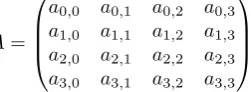
II. THEADVANCEDENCRYPTIONSTANDARD The round transformation of the AES operates on a 128 -bit intermediate result, called state. The state is internally represented as a 4×4array of bytes A:
A=
a0,0 a0,1 a0,2 a0,3
a1,0 a1,1 a1,2 a1,3
a2,0 a2,1 a2,2 a2,3
a3,0 a3,1 a3,2 a3,3
.
Each byte ai,j, 0 ≤ i, j ≤ 3, is considered as an element
of F28 ∼=F2[x]/(m(x)), where the irreducible polynomial is
given by m(x) = x8+x4+x3+x+ 1. In the following,
we encode an element of F28 by two hexadecimal digits: for
instance, 89 is equivalent to x7+x3+ 1 in the polynomial
basis representation. We denote the jth column of A by Aj.
The number of rounds Nr as well as the number of 32-bit
blocks in the cipher keyNk of the AES depend on the desired
security level (Table I).
TABLE I
BLOCK LENGTH,KEY LENGTH,NUMBER OF32-BIT BLOCKS OF THE KEY (Nk),AND NUMBER OF ROUNDS(Nr)OFAES-128, AES-192,AND
AES-256.
Algorithm Block length[bits] Key length[bits] Nk Nr
AES-128 128 128 4 10
AES-192 128 192 6 12
AES-256 128 256 8 14
The AES involves four byte-oriented transformations and their inverses for encryption and decryption, respectively [13]:
• TheSubBytesstep is the only non-linear transformation of the AES. Its role is to introduce confusion to the data so that the relationship between the secret key and the ciphertext is obscured. It updates each byte of the state using an 8-bit S-box, denoted by SRD. Internally,
the AES S-box computes the modular inverse ofai,j (the
The inverse transformation, calledInvSubBytesand de-noted by S−RD1, performs the inverse affine transformation followed by an inversion overF28.
• TheShiftRowsstep simply consists of a cyclical left shift of the three bottom rows of the state by1,2, and3bytes, respectively:
b0,j
b1,j
b2,j
b3,j
←
a0,j
a1,(j+1) mod 4
a2,(j+2) mod 4
a3,(j+3) mod 4
,
where 0 ≤ j ≤ 3. The inverse operation is called InvShiftRows:
a0,j
a1,j
a2,j
a3,j
←
b0,j
b1,(j+3) mod 4
b2,(j+2) mod 4
b3,(j+1) mod 4
.
• TheMixColumnsstep is a permutation operating on the AES state column by column. Together withShiftRows, this step provides diffusion in the cipher: if a single bit of the plaintext is flipped, then the whole ciphertext should be changed. Each column of the AES state is considered as a polynomial overF28, and is multiplied moduloy4+
01 by the constant polynomial c(y) = 03·y3+01· y2+01·y+02 [13]. This operation is performed by multiplying each column of the state A by a circulant matrixME:
b0,j
b1,j
b2,j
b3,j
←
02 03 01 01
01 02 03 01
01 01 02 03
03 01 01 02
| {z }
ME ·
a0,j
a1,j
a2,j
a3,j
,
where0≤j≤3.
During the inverse operation, called InvMixColumns, each column of the state is multiplied by d(y) = 0B· y3+0D·y2+09·y+0E. One easily checks thatd(y)
is the multiplicative inverse of c(y)moduloy4+ 1:
c(y)·d(y)≡01 (mody4+ 1).
Here again, the modular multiplication by a constant polynomial can be defined by a matrix multiplication:
b0,j
b1,j
b2,j
b3,j
←
0E 0B 0D 09
09 0E 0B 0D
0D 09 0E 0B
0B 0D 09 0E
| {z }
MD ·
a0,j
a1,j
a2,j
a3,j
.
• The AddRoundKey step combines the state A with a 128-bit round key. Let r denote the round index. Each byteki,4r+j of the round key and its corresponding byte
ai,jare added inF28 by a simple bitwise XOR operation.
AddRoundKey is therefore its own inverse.
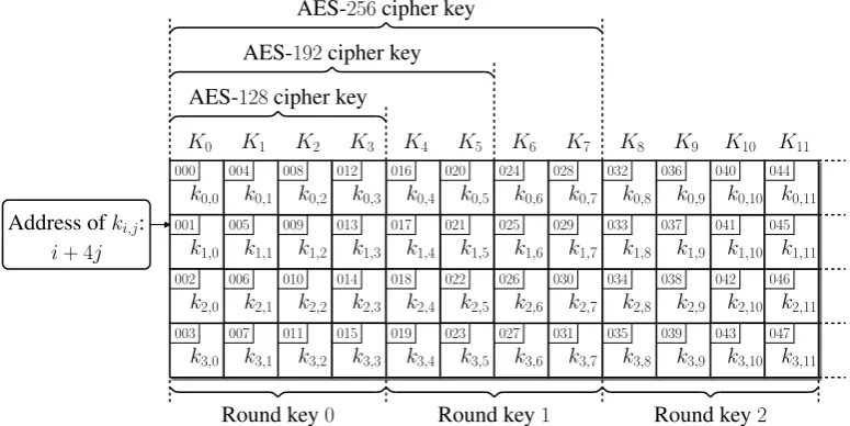
A. Key Expansion
The round keys involved in the AddRoundKey steps are derived from the cipher key as follows. Let us consider an array consisting of 4 rows and 4·(Nr+ 1) columns. Each
column Kj contains four elements of F28 denoted by k0,j,
k1,j, k2,j, and k3,j. The round key of the jth round of the
AES encryption algorithm is given by columnsK4j toK4j+3
(Figure 1).
The cipher key is copied in the firstNkcolumns of the array,
and the next columns are defined recursively. The process, summarized by Algorithms 1 and 2, involves an intermediate variable RC ∈ F28 and a permutation matrix P defining a
cyclic rotation of the bytes within a column:
P =
00 01 00 00
00 00 01 00
00 00 00 01
01 00 00 00
.
We denote the identity matrix byI. This matrix notation will be useful to pinpoint a unified8-bit datapath for key expansion, encryption, and decryption in Section IV-A.
Algorithm 1 AES key expansion forNk ≤6. Input: A cipher keyK0, . . . ,KNk−1. Output: Expanded key.
1. RC←x0;
2. forj=Nk to4Nr+ 3do 3. ifjmodNk = 0then
4. Kj ← P ·
SRD(k0,j−1)
SRD(k1,j−1)
SRD(k2,j−1)
SRD(k3,j−1)
⊕ I ·Kj−Nk;
5. k0,j ←k0,j⊕RC; 6. RC←x·RC; 7. else
8. Kj ← I ·Kj−1⊕ I ·Kj−Nk;
9. end if
10. end for
11. ReturnKNk, . . . ,K4Nr+3;
B. Encryption
After an initial AddRoundKey step, an AES encryption involvesNr−1 repetitions of a round composed of the four
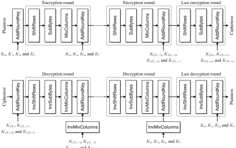
byte-oriented transformations described above. Eventually, a final encryption round, in which the MixColumns step is omitted, produces the ciphertext (Algorithm 3). Noting that the order ofShiftRowsandSubBytesis indifferent [13], we obtain the datapath depicted on Figure 2.
Algorithm 3 updates the AES state column by column. Since the ShiftRows transformations performs cyclical left shifts of the three bottom rows of the state, we have to be careful not to overwrite bytes that are still involved in the forthcoming MixColumns steps (a1,0 is for instance needed
k3,1 006 039 037 038 036
k3,9 k1,9
k2,9 k0,9 K9 K5
005
K6
007
K7 K8
k0,0
k2,0 k1,0
K10
043 041
042 040
k3,10 k1,10
k2,10 k0,10 AES-128cipher key
AES-192cipher key AES-256cipher key
Round key0 Round key1 Round key2
k3,0
016
k3,4 k1,4
k2,4 k0,4 Address ofki,j:
018 000
017
i+ 4j
K0
019 k0,3
k2,3
023 021
022 020
k3,5 k1,5
k2,5 k0,5
002
k1,3 001
k3,3 003 K11 012 014 013 027 025 026 024
k3,6 k1,6
k2,6 k0,6
047 015
045 k0,2
046 044
k2,2 k1,2
k3,2
031 029
030 028
k3,7 k1,7
k2,7 k0,7
k3,11 008
k1,11
010
k2,11 k0,11
009
011 k0,1
035 033
034 032
k3,8 k1,8
k2,8 k0,8 K1
k2,1 K2
k1,1
K3 K4
004
Fig. 1. Key expansion and round selection.
Algorithm 2 AES key expansion forNk>6. Input: A cipher keyK0, . . . ,KNk−1. Output: Expanded key.
1. RC←x0;
2. forj=Nk to4Nr+ 3 do 3. if jmodNk= 0 then
4. Kj← P ·
SRD(k0,j−1)
SRD(k1,j−1)
SRD(k2,j−1)
SRD(k3,j−1)
⊕ I ·Kj−Nk;
5. k0,j ←k0,j⊕RC; 6. RC←x·RC;
7. else ifjmodNk = 4then
8. Kj← I ·
SRD(k0,j−1)
SRD(k1,j−1)
SRD(k2,j−1)
SRD(k3,j−1)
⊕ I ·Kj−Nk;
9. else
10. Kj← I ·Kj−1⊕ I ·Kj−Nk; 11. end if
12. end for
13. Return KNk, . . . ,K4Nr+3;
encryption algorithm requires an internal4×4 array of bytes B.
C. Decryption
We consider here the equivalent decryption algorithm de-scribed in [13, Section 3.7.3] (Algorithm 4). Its main ad-vantage over the straightforward decryption process is that encryption and decryption rounds share the same datapath (Figure 2). Nevertheless, the round keys are introduced in reverse order for decryption.
Algorithm 3 AES encryption.
Input: A128-bit plaintextA andNr+ 1 round keys. Output: A128-bit ciphertextB.
1. forj= 0to3 do 2. Aj← I ·Aj⊕ I ·Kj; 3. end for
4. fori= 1 toNr−1 do 5. forj= 0to3 do
6. Bj← ME·
SRD(a0,j)
SRD(a1,(j+1) mod 4)
SRD(a2,(j+2) mod 4)
SRD(a3,(j+3) mod 4)
⊕ I ·K4i+j;
7. end for
8. A←B;
9. end for
10. forj= 0to3 do
11. Bj ← I ·
SRD(a0,j)
SRD(a1,(j+1) mod 4)
SRD(a2,(j+2) mod 4)
SRD(a3,(j+3) mod 4)
⊕ I ·K4Nr+j;
12. end for 13. ReturnB;
III. THEHASHFUNCTIONECHO
The ECHO family of hash functions [5] is built around the round function of the AES. This design strategy allows one to easily exploit advances in the implementation of the AES, such as the new AES instruction set of Intel Westmere processors [6]. ECHO is a family of four hash functions, namely ECHO-224, ECHO-256, ECHO-384, and ECHO-512 (Table II). The main differences lie in the length of the chaining variable and in the number of rounds.
K4Nr,K4Nr+1,
K4Nr+2, andK4Nr+3 K4Nr−2, andK4Nr−1
K4Nr−4,K4Nr−3, K4,K5,K6, andK7
K0,K1,K2, andK3
AddRoundK
e
y
AddRoundK
e
y
AddRoundK
e
y
Cipherte
xt
Plainte
xt
Encryption round
SubBytes
ShiftRo
ws
MixColumns
Encryption round
SubBytes
ShitfRo
ws
MixColumns
Last encryption round
AddRoundK
e
y
SubBytes
ShiftRo
ws
K4Nr,K4Nr+1,
K4Nr+2, andK4Nr+3
K0,K1,K2, andK3
AddRoundK
e
y
K4,K5,K6, andK7 K4Nr−4,K4Nr−3,
K4Nr−2, andK4Nr−1
In
vShiftRo
ws
In
vSubBytes
Last decryption round
In
vMixColumns
In
vShiftRo
ws
In
vSubBytes
Decryption round
In
vMixColumns
In
vShiftRo
ws
In
vSubBytes
Decryption round
Cipherte
xt
Plainte
xt
InvMixColumns InvMixColumns
AddRoundK
e
y
AddRoundK
e
y
AddRoundK
e
y
Fig. 2. AES encryption and decryption flowcharts.
Algorithm 4 AES decryption.
Input: A128-bit ciphertextA andNr+ 1 round keys. Output: A128-bit plaintext B.
1. forj= 0 to3do
2. Aj ← I ·Aj⊕ I ·K4Nr+j; 3. end for
4. fori= 1toNr−1do 5. forj= 0 to3do
6. Bj← MD·
S−RD1(a0,j)
S−RD1(a1,(j+3) mod 4)
S−RD1(a2,(j+2) mod 4)
S−RD1(a3,(j+1) mod 4)
⊕MD·K4Nr−4i+j;
7. end for
8. A←B;
9. end for
10. forj= 0 to3do
11. Bj← I ·
S−RD1(a0,j)
S−RD1(a1,(j+3) mod 4)
S−RD1(a2,(j+2) mod 4)
S−RD1(a3,(j+1) mod 4)
⊕ I ·Kj;
12. end for 13. Return B;
interface for ECHO (and several other hash functions) com-prising communication and padding is for instance described
TABLE II
PROPERTIES OF THEECHOFAMILY OF HASH FUNCTIONS(REPRINTED FROM[5]). ALL SIZES ARE GIVEN IN BITS.
Algorithm Chainingvariable Messageblock Digest Counter Salt
ECHO-224 512 1536 224 64or128 128
ECHO-256 512 1536 256 64or128 128
ECHO-384 1024 1024 384 64or128 128
ECHO-512 1024 1024 512 64or128 128
in [4]. A padded message is divided into 1536-bit (ECHO-224and ECHO-256) or1024-bit (ECHO-384and ECHO-512) message blocksM1,M2, . . . ,Mtthat are iteratively processed
using a compression functionCompress512 (ECHO-224and
ECHO-256) orCompress1024 (ECHO-384 and ECHO-512).
The internal stateSiof the ECHO family can be viewed as
a4×4array of128-bit words (Figure 3), each of them being considered as an AES stateA(k),0≤k≤15:
• ECHO-224/256. The 512-bit chaining variableVi−1 and
the 1536-bit message blockMi,1≤i≤t, are split into
Nv = 4 andNm= 12 AES states, respectively.Vi−1 is
stored in the first column of the internal state, andMiin
the remaining columns.
• ECHO-384/512. Both Vi−1 and Mi are 1024-bit values
that can be split into Nv =Nm = 8 AES states. Vi−1
occupies the first half of the internal state and Mi the
Vi−1 Mi
Vi−1 Mi
ECHO-224/256:
ECHO-384/512:
Address ofa(i,jk): i+ 4j+ 16k
a(2)2,2 a(2)2,0
a(2)0,0 a(2)0,1
a(2)2,1
A(0) A(1) A(4) A(5) A(8) A(9) A(12) A(13)
A(2) A(6)
A(3) A(7) A(11)
A(10) A(14)
A(15) 003 014 013 015 011 007 012 008 009 005 010 001 002 000 004 006
a(0)3,0
a(0)2,3 a(0)1,3
a(0)3,3 a(0)3,2 a(0)3,1
a(0)0,3 a(0)0,2
a(0)1,2 a(0)1,1
a(0)2,2 a(0)1,0
a(0)2,0 a(0)0,0 a(0)0,1
a(0)2,1
035 046 045 047 043 039 044 040 041 037 042 033 034 032 036 038
a(2)3,0
a(2)2,3 a(2)1,3
a(2)3,3 a(2)3,2 a(2)3,1
a(2)0,3 a(2)0,2
a(2)1,2 a(2)1,1 a(2)1,0
Fig. 3. Internal state of the ECHO family.
The initial chaining variable V0 encodes the intended hash
output size [5, Section 2.1].
BIG.ShiftRows BIG.MixColumns BIG.SubWords BIG.SubWords BIG.MixColumns BIG.ShiftRows T V0
Mt Ct Salt
M1 C1 Salt
Compress1024
Compress512or
Vt V1
Fig. 4. Chained iteration of the compression function.Tdenotes the optional truncation described in [5, Section 3.5] and [5, Section 4.1].
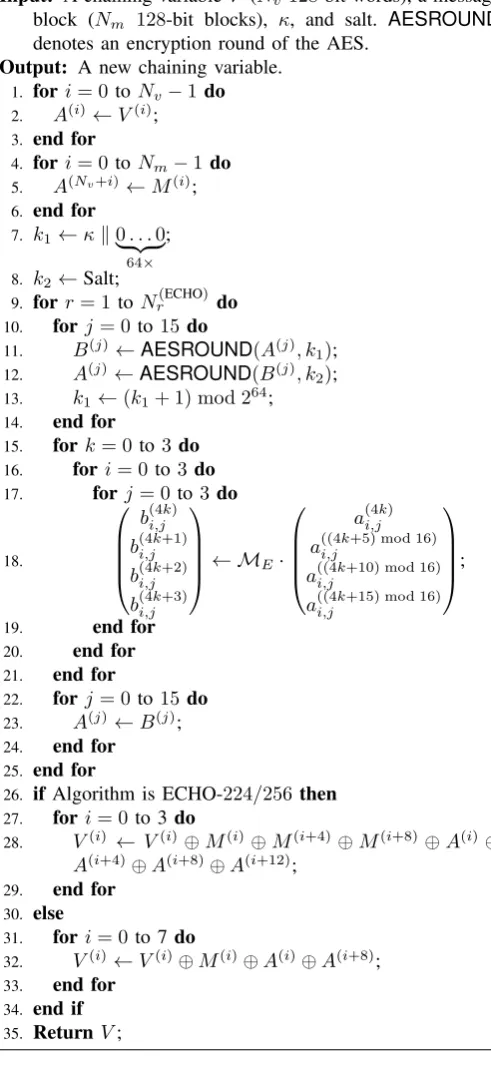
ECHO applies iteratively a compression function to update the chaining variableVi,0≤i≤t(Figure 4 and Algorithm 5).
Compress512 andCompress1024 performN (ECHO)
r = 8 and
10iterations of BIG.Round, respectively.BIG.Round is the sequential composition of three transformations:
• The BIG.SubWords transformation applies two AES rounds to each 128-bit word A(j), 0 ≤j ≤15, of the
internal state defined on Figure 3:
A(j)←AESROUND(AESROUND(A(j), k1), k2),
where AESROUND denotes one round of the AES encryption flow. As explained in Section II-B, an internal 4 × 4 array of bytes B(j) is needed to solve data
dependency issues (Algorithm 5, lines 11 and 12). The key schedule for the derivation of the two 128-bit subkeys k1 andk2 is much simpler than the one of the
AES. k1 is related to the number of unpadded message
bits Ci hashed at the end of the current iteration. An
internal 64-bit counter κ is initialized with the value of Ci, andk1 is defined as follows:
k1=κk0. . .0
| {z }
64× .
κis incremented at the end of each AES round involving k1. If the size of the message exceeds 264−1, one has
the flexibility to use a 128-bit counter Ci. k2 is equal
to the 128-bit salt value that enables ECHO to support randomized hashing.
• The BIG.ShiftRows step is the analogue of the Shift-Rowsstep of the AES. The first line of the internal state is left unchanged. Each128-bit word of the second, third, and fourth lines is left-rotated by one, two, and three po-sitions, respectively. At the byte level, this transformation is given by:
b(4i,jk)
b(4i,jk+1)
b(4i,jk+2) b(4i,jk+3)
←
a(4i,jk)
a((4i,jk+5) mod 16)
a((4i,jk+10) mod 16) a((4i,jk+15) mod 16)
,
where0≤i, j, k≤3.
• The BIG.MixColumnsstep operates on the ECHO state column by column. We build a polynomial over F28 by
picking the (i+ 4j)th byte of each AES state in thekth column, and apply to it theMixColumnstransformation:
b(4i,jk)
b(4i,jk+1) b(4i,jk+2)
b(4i,jk+3) ←
02 03 01 01 01 02 03 01 01 01 02 03 03 01 01 02
·
a(4i,jk)
a(4i,jk+1) a(4i,jk+2)
a(4i,jk+3) ,
where 0≤i, j, k ≤3. We combine the BIG.ShiftRows andBIG.MixColumns steps (Algorithm 5, line 18), and avoid data dependency issues thanks to intermediate variablesB(j),0≤j≤15.
After Nr(ECHO) calls to the compression function, the
BIG.Final step generates the new value of the chaining vari-able Vi fromVi−1, Mi, and the internal state. Note that this
step depends on the selected level of security (Algorithm 5, lines 26 to 34).
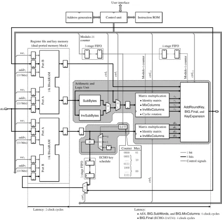
IV. A COMPACTUNIFIEDCOPROCESSOR FOR THEAES AND THEECHO FAMILY OFHASHFUNCTIONS A. A Unified Arithmetic and Logic Unit
Algorithm 5 The ECHO hash function.
Input: A chaining variableV (Nv 128-bit words), a message
block (Nm 128-bit blocks), κ, and salt. AESROUND
denotes an encryption round of the AES. Output: A new chaining variable.
1. fori= 0toNv−1 do 2. A(i)←V(i);
3. end for
4. fori= 0toNm−1 do 5. A(Nv+i)←M(i); 6. end for
7. k1←κk0. . .0
| {z }
64× ;
8. k2←Salt;
9. forr= 1toNr(ECHO)do 10. forj= 0 to15do
11. B(j)←AESROUND(A(j), k 1);
12. A(j)←AESROUND(B(j), k 2);
13. k1←(k1+ 1) mod 264;
14. end for
15. fork= 0to3 do 16. fori= 0 to3do 17. forj= 0 to3do
18.
b(4i,jk)
b(4i,jk+1)
b(4i,jk+2)
b(4i,jk+3)
← ME·
a(4i,jk)
a((4i,jk+5) mod 16)
a((4i,jk+10) mod 16)
a((4i,jk+15) mod 16) ;
19. end for
20. end for
21. end for
22. forj= 0 to15do 23. A(j)←B(j);
24. end for
25. end for
26. if Algorithm is ECHO-224/256 then 27. fori= 0 to 3 do
28. V(i) ←V(i)⊕M(i)⊕M(i+4)⊕M(i+8)⊕A(i)⊕ A(i+4)⊕A(i+8)⊕A(i+12);
29. end for
30. else
31. fori= 0 to 7 do
32. V(i)←V(i)⊕M(i)⊕A(i)⊕A(i+8);
33. end for
34. end if 35. Return V;
Unit (ALU). We can now describe key expansion (Algo-rithms 1 and 2), encryption (Algorithm 3), and decryption (Algorithm 4) using a single instruction:
Rk ← A ·f(Ri)⊕ B ·Rj, (1)
where
• Ri,Rj, andRk are vectors of four bytes;
• f is a function applied to each byte of Ri;
• A andB are4×4 matrices of bytes.
The values of these parameters for the different steps of Algorithms 1, 2, 3, and 4 are summarized in Table III. The hash function ECHO benefits from the same instruc-tion: the BIG.SubWords consists of AES rounds, and the BIG.MixColumns step involves the circulant matrix ME.
Only the key schedule and theBIG.Finalstep require a small additional amount of hardware.
1) TheSubBytesandInvSubBytesSteps: TheSubBytes and InvSubBytes steps are often considered as the most critical part of the AES and several architectures for SRDand
S−RD1 have already been described in the literature (see for instance [20] for a comprehensive bibliography). On Xilinx Virtex-5and Virtex-6FPGAs, the best design strategy consists in implementing the AES S-boxes as8-input tables [12]. Two control bits ctrl1:0 allow us to perform SubBytes,
InvSub-Bytes, or to bypass this stage whenf is the identity function. 2) Matrix Multiplication: A quick look at Table III in-dicates that matrix A in Equation (1) can be any of the four matrices introduced in Section II. Two control bits ctrl3:2 are therefore necessary to select the desired operation.
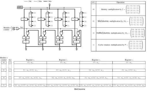
Since we emphasize reducing the usage of FPGA resources, we adopt the multiply-and-accumulate approach proposed by H¨am¨al¨ainenet al.[24], and need4clock cycles to multiply one column of the state or the round key array by a4×4circulant matrix (Figure 6). Let us consider the productME·Aj. We
compute a first partial product by multiplying each coefficient of the fixed polynomial01+01·y+03·y2+02·y3bya0,j,
and store the result in registersr0,r1,r2, andr3. Then, at each
clock cycle, the intermediate result is rotated and accumulated with a new partial product. This process involves a control signal to distinguish between the first step and the subsequent ones. Such a signal can be generated by computing the bitwise OR of the two bits of a modulo-4 counter.
A standard way to implement the AES consists in taking ad-vantage of the well-known relation between theMixColumns andInvMixColumnspolynomials [13, p. 55]:
d(y) = (04y2+05)·c(y) mod (y4+01).
However, multiplication by 04y2 + 05 would incur extra clock cycles for decryption (i.e. a different instruction flow for encryption and decryption). In order to keep the instruction memory of our coprocessor as small as possible, it is crucial to use the same code for encryption and decryption. A status register indicates which algorithm is currently executed, and the control unit generates the control bitsctrl3:0 accordingly.
Our algorithm for multiplication by MD is based on the
following observation [29]:
MD=ME +
0C 08 0C 08 08 0C 08 0C 0C 08 0C 08 08 0C 08 0C
.
Table IVa defines the multiplication of an element a(x) = P7
i=0aix i ∈
F28 by 08 and 0C. Note that each line of the
TABLE III
IMPLEMENTATION OFAESKEY EXPANSION, AESENCRYPTION, AESDECRYPTION,ANDBIG.MIXCOLUMNSWITH A SINGLE INSTRUCTION.
Algorithm Operation Rk A f Ri B Rj
Algorithm 1, line 4 Ki P SRD Ki−1 I Ki−Nk
Key expansion Algorithm 1, line 8 Ki I Identity Ki−1 I Ki−Nk
Algorithm 2, line 8 Ki I SRD Ki−1 I Ki−Nk
Algorithm 3, line 2 Aj I Identity Aj I Kj
AES encryption Algorithm 3, line 6 Bj ME SRD
a0,j a1,(j+1) mod 4 a2,(j+2) mod 4 a3,(j+3) mod 4
I K4i+j
Algorithm 3, line 11 Bj I SRD
a0,j a1,(j+1) mod 4 a2,(j+2) mod 4 a3,(j+3) mod 4
I K4Nr+j
Algorithm 4, line 2 Aj I Identity Aj I K4Nr+j
AES decryption Algorithm 4, line 6 Bj MD S−1RD
a0,j a1,(j+3) mod 4 a2,(j+2) mod 4 a3,(j+1) mod 4
MD K4Nr−4i+j
Algorithm 4, line 11 Bj I S−1RD
a0,j a1,(j+3) mod 4 a2,(j+2) mod 4 a3,(j+1) mod 4
I Kj
BIG.MixColumns Algorithm 5, line 18
b(4i,jk) b(4i,jk+1)
b(4i,jk+2)
b(4i,jk+3)
ME Identity
a(4i,jk) a((4i,jk+5) mod 16)
a((4i,jk+10) mod 16)
a((4i,jk+15) mod 16)
I
00 00 00 00
implemented by means of a LUT with5inputs and2outputs (i.e. a LUT6 2 primitive if we consider Virtex-5 or Virtex-6 FPGAs). A second table computes(00·y2+00·y3)·a(x), (00·y2+01·y3)·a(x),(01·y2+00·y3)·a(x), or(03·y2+
02·y3)·a(x)according to the2control bitsctrl
3:2. Since the
computation of each digit of02·a(x)and03·a(x)requires at most3 coefficients ofa(x)(Table IVb), this operation can be implemented by means of8LUT6 2 primitives.
Figure 7 describes how we implement multiplication byI, ME,MD, andP by combining the outputs of those tables.
One easily checks that this circuit is equivalent to the one illustrated in Figure 6. In particular, note that the content of registers r2 andr3 is given by:
r2←
00 ifctrl3:2= 00,
03·a(x) ifctrl3:2= 01,
(08⊕03)·a(x) =0B·a(x) ifctrl3:2= 10,
01·a(x) ifctrl3:2= 11,
and
r3←
01·a(x) ifctrl3:2= 00,
02·a(x) ifctrl3:2= 01,
(0C⊕02)·a(x) =0D·a(x) ifctrl3:2= 10,
00 ifctrl3:2= 11.
Our matrix multiplication unit involves16LUT6 2 primitives and 32 LUT6 primitives, resulting in a total requirement of 12slices on a Virtex-5 FPGA. Compared to theMixColumns
operator of ECHO-256 coprocessor described in [8], where only multiplication byME is needed, the hardware overhead
amounts to 4 Virtex-5 slices. Matrix B is either the identity matrix I or theInvMixColumnsmatrix MD (Table III). We
followed a similar strategy to implement multiplication byB. 3) Addition overF28: Figure 8 describes the component we
designed to perform theAddRoundKeystep. Since our matrix multiplication units output 4 bytes, we perform 4 additions over F28 in parallel and store the result in a shift register.
This approach allows us to write data byte by byte in the register file. Here again, a simple modulo-4 counter controls the process: a new result is loaded during the first clock cycle, and then shifted in the three subsequent clock cycles.
The same component performs the additions involved in the round key derivation. However, additional hardware resources are needed to:
• initialize RC (Algorithm 1, line 1 and Algorithm 2, line 1);
• add RC tok0,iwhen the column indexiis a multiple of
Nk (Algorithm 1, line 5 and Algorithm 2, line 5);
• update RC (Algorithm 1, line 6 and Algorithm 2, line 6).
A multiplexer controlled by ctrl6 selects the operand loaded
in the register when the clock enable signal ctrl7 is equal to
1: the initial value 01 or x·RC. When imodNk = 0, the
control unit sets ctrl8 to1so that RC is added to k0,i.
BIG.Final, and
KeyExpansion
Data
ctrl
9
User interface
4-stage FIFO
18
k
BlockRAM
18
k
BlockRAM
3-stage FIFO
Modulo-4
counter
Modulo-4
counter
AddRoundKey, Logic Unit
10
Arithmetic and
00
ECHO key
01
Mux
schedule (10bits)
0001
1111
. . .
1000 0111
(10bits)
. . . (10bits)
0000
Counter LUT
5
-stage
FIFO
ctrl
8:4
ctrl
3:2
ctrl
0
ctrl
1
counter Modulo-16
(10bits)
Latency:2clock cycles
Control unit Instruction ROM
1 0
Address generation
r3
r2
r1
r0
sk3
sk2
sk1
Latency:
•AES,BIG.SubWords, andBIG.MixColumns:6clock cycles
•BIG.Final(ECHO-384/512):2clock cycles
sk0
•BIG.Final(ECHO-224/256):4clock cycles
8bits
Control signals
1bit
SubBytes
Port
A
Port
B
we0
(dual-ported memory block) Register file and key memory
we1
addr1
addr0
Port
B
Port
A
we3
we2
addr2
addr3
InvSubBytes 0 1
01 00
10 1 0
1 0
ctrl
10
Matrix multiplication
•Identity matrix
•InvMixColumns
Matrix multiplication
•Identity matrix
•MixColumns
•InvMixColumns
•Cyclic rotation
Fig. 5. General architecture of our unified8-bit coprocessor for AES and ECHO.
the constant00stored in the key memory of the coprocessor. During the BIG.Final step, two bytes are read from the register file at each clock cycle, and accumulated thanks to the feedback mechanism controlled by ctrl4 and ctrl5 (here
again, the signal sk0 is obtained by reading the constant 00
from the key memory). Thus, the computation of each byte of V(i) involves four and two clock cycles for ECHO-224/256 and ECHO-384/512, respectively. All other operations require six clock cycles (Figure 5). Therefore, special attention must be paid to the design of the control unit in order to take the latency of each operation into account.
4) ECHO key schedule: The choice of an 8-bit datapath enables to increment the internal 64-bit counter κin8 clock cycles, thus keeping the critical path of the adder as small as
possible. Figure 5 describes the pipelined adder implementing ECHO key schedule. k1 is stored in the key memory and
is read byte by byte. During the first clock cycle, we add the constant 1 to the least significant byte of k1 and store
the output carry in a flip-flop. This carry bit is then added to the second byte of k1, and the content of the flip-flop is
updated accordingly. We repeat this process until the 64least significant bits ofk1 are updated. Since the8most significant
bytes ofk1are not modified, we simply add the constant0in
1
MixColumns: multiplication byME=
02 03 01 01 01 02 03 01 01 01 02 03 03 01 01 02
Identity: multiplication byI=
01 00 00 00 00 01 00 00 00 00 01 00 00 00 00 01
Cyclic rotation: multiplication byP=
00 01 00 00 00 00 01 00 00 00 00 01 01 00 00 00
InvMixColumns: multiplication byMD=
0E 0B 0D 09 09 0E 0B 0D 0D 09 0E 0B 0B 0D 09 0E
Operation
ctrl3:2
00
01
10
11 1bit 2bits 8bits
Modulo-4
counter
MixColumns 00
01
10
11
counter Modulo-4
0
1
1
01
09 00
00
11 10 01 00
02
0E 01
00
11 10 01 00
01
0D 00
00
11 10 01 00
03
0B 00
01
11 10 01 00
ctrl3:2
T
ime
r1 r2 r3
01·a0,j⊕01·a1,j⊕02·a2,j Acc
Registerr3
03·a0,j⊕01·a1,j⊕01·a2,j
Registerr2
01·a0,j⊕02·a1,j⊕03·a2,j⊕01·a3,j
02·a0,j 03·a0,j
01·a0,j 01·a0,j
02·a0,j⊕03·a1,j⊕01·a2,j⊕01·a3,j
Registerr1
Acc Registerr0
01·a0,j⊕02·a1,j 02·a0,j⊕03·a1,j
03·a0,j⊕01·a1,j 01·a0,j⊕01·a1,j
01·a0,j⊕02·a1,j⊕03·a2,j
01·a0,j⊕01·a1,j⊕02·a2,j⊕03·a3,j 02·a0,j⊕03·a1,j⊕01·a2,j
03·a0,j⊕01·a1,j⊕01·a2,j⊕02·a3,j r0
Fig. 6. Multiplication by a circulant matrix. TABLE IV
MULTIPLICATION OVERF28OFa(x)BY SEVERAL CONSTANTS.
Inputs ×08 ×0C
a5,a6 a5 a5⊕a6
a5,a6,a7 (a5⊕a6)x (a5⊕a7)x
a0,a6,a7 (a6⊕a7)x2 (a0⊕a6)x2
a0,a1,a5,a6,a7 (a0⊕a5⊕a7)x3 (a0⊕a1⊕a5⊕a6⊕a7)x3 a1,a2,a5,a6,a7 (a1⊕a5⊕a6)x4 (a1⊕a2⊕a5⊕a7)x4
a2,a3,a6,a7 (a2⊕a6⊕a7)x5 (a2⊕a3⊕a6)x5
a3,a4,a7 (a3⊕a7)x6 (a3⊕a4⊕a7)x6
a4,a5 a4x7 (a4⊕a5)x7
(a) Multiplication ofa(x)by08and0C.
Inputs ×01 ×02 ×03
a0,a7 a0 a7 a0⊕a7
a0,a1,a7 a1x (a0⊕a7)x (a0⊕a1⊕a7)x
a1,a2 a2x2 a1x2 (a1⊕a2)x2
a2,a3,a7 a3x3 (a2⊕a7)x3 (a2⊕a3⊕a7)x3 a3,a4,a7 a4x4 (a3⊕a7)x4 (a3⊕a4⊕a7)x4
a4,a5 a5x5 a4x5 (a4⊕a5)x5
a5,a6 a6x6 a5x6 (a5⊕a6)x6
a6,a7 a7x7 a6x7 (a6⊕a7)x7
(b) Multiplication ofa(x)by02and03.
B. Memory Organization
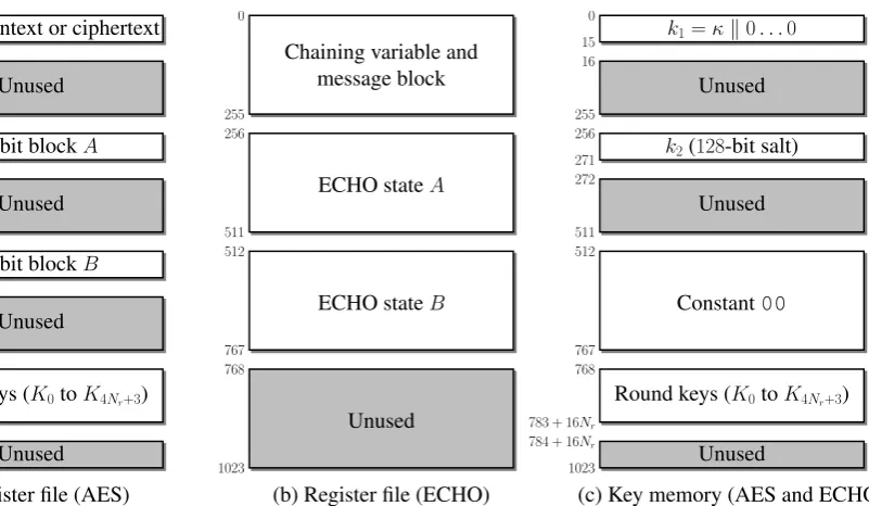
Since we consider an 8-bit datapath, the memory of our coprocessor is organized into bytes. We will show below that 10 address bits are needed to access message blocks and intermediate data, thus allowing us to implement the register file and the key memory by means of a single Virtex-5 or Virtex-6 block RAM configured as two independent 18 Kb RAMs (Figure 5).
a) Register file.: Recall that an ECHO state is an array of 256 bytes a(i,jk), where 0 ≤ i, j ≤ 3 and 0 ≤ k ≤ 15 (Figure 3). Let us define the8-bit address ofa(i,jk)as16k+4j+i (i.e. the 4 most significant bits encode the index k, and the 4 least significant bits define the location of the byte in the AES stateA(k)). We decided to organize the register file into
four blocks of 256 bytes selected by two additional address
bits (Figure 9). In order to implement ECHO according to Algorithm 5, we need a first4×4array of AES states to store the chaining variable and the message block. The compression function involves two additional arrays (ECHO statesAandB in Algorithm 5). We use the128least significant bits ofAand B as intermediate variables for the AES. The key expansion algorithm computesKifromKi−1andKi−Nk (Algorithms 1 and 2). In order to access a byte ofKi−1andKi−Nk at each clock cycle, we keep two copies of the round keys. The first one is located in the 4th block of 256 bytes of the register file, and the second one is stored in the key memory. Since Nr≤14, we have to memorize at most4Nr+4 = 60columns
Ki, i.e. 240 bytes. The 8 least significant address bits of a
round key byte ki,j, 0 ≤ i≤ 3 and 0 ≤j ≤Nr ≤14, are
11
Modulo-4 counter
00
00
8LUT6 2 8LUT6 2
ctrl3
8LUT6
8LUT6 8LUT6 ctrl
2 8LUT6
a(x)
11 10 11 10
00 00
01 00
00 00
01 00
00
01 10
ctrl3:2
ctrl3:2
11 00
8bits
01 10 1bit 2bits
r1
×09 ×0D
×02 ×0C
r3 ×08
r2
r0
×03
Fig. 7. Multiplication byI,ME,MD, andP.
Computation of RC
ctrl4
5
-input LUTs
2-input LUTs
×x
ctrl7
ctrl5
Modulo-4 counter
ctrl8 1 0
1bit 8bits
1 0
ctrl6
(key expansion)
1 0
To register file 01
0 1
00
RC or00
r3 r2
r1
r0 sk1 sk2 sk3
register file From
sk0
LUTs
6
-input
ctrl4
1 0 1 0
4-input LUTs
16
Unused
512 0
255
message block Chaining variable and
767 256
511
ECHO stateA
Constant00 512
767
ECHO stateB
272 272
128-bit blockB 512
527
Unused 767
528
Unused 784 + 16Nr
1023
Round keys (K0toK4Nr+3)
783 + 16Nr
768
Unused 784 + 16Nr
1023
Unused 255
511 16
Unused 271
256
k2(128-bit salt)
(c) Key memory (AES and ECHO) (a) Register file (AES)
768
1023
Unused
(b) Register file (ECHO)
15 0
k1=κk0. . .0
511
Unused
768 271
256
128-bit blockA
783 + 16Nr
15 0
128-bit plaintext or ciphertext
Round keys (K0toK4Nr+3)
255
Fig. 9. Memory organization.
b) Key memory.: Besides a copy of the AES round keys, the key memory contains k1, k2, and a block whose all
bytes are set to zero which provides us with the constant 00 needed for the BIG.MixColumns and BIG.Final steps (Section IV-A3). Thus, no dedicated hardware is needed to forcesk0,sk1,sk2, andsk3 to00.
In the following, we show that our careful organization of the data in the register file and in the key memory allows one to design a control unit based on a4-bit counter, an8-bit counter, and a simple Finite State Machine (FSM).
C. Control Unit
The control bits of our unified ALU, the read and write addresses of the register file and the key memory, and the write enable signals are computed by a control unit that mainly consists of an address generator and an instruction memory. A FSM, four internal registers, and a stack allow us to select and execute the algorithm specified by the user.
1) Address Generation: The address generation process is the most challenging task in the design of a low-area unified coprocessor for the AES and the hash function ECHO: at first glance, it seems that each task (AES key expansion, AES encryption, AES decryption,BIG.MixColumns, etc.) requires a different addressing scheme. However, we described a way to generate the eight least significant bits of all read and write addresses of ECHO-256 by means of a counter by5 modulo 16 and a modulo-256 counter [8]. We show here that our address generator can be slightly modified in order to support ECHO-512 and the AES (Figures 10 and 11). Note that our control unit generates at each clock cycle a read address and its corresponding write address. Since our coprocessor embeds several pipeline stages (Figure 5), it is necessary to delay write addresses and write enable signals accordingly. Shift registers allow us to synchronize signals in our coprocessor. On Xilinx
devices, they are efficiently implemented by means of SRL16 primitives, whose depth is dynamically adjusted according to the algorithm being executed (Figure 10c): the latency of the BIG.Finalstep is equal to six and four clock cycles for ECHO-224/256 and ECHO-384/512, respectively. In all other cases, the datapath includes eight pipeline stages.
Figure 10 describes the generation of the write enable signals and the two most significant bits of read and write addresses. The architecture is fairly simple in the case of the key memory: two control bitsctrl6:5 allows for selecting one
of the four blocks of256bytes. For a given algorithm, read and write operations always occur in the same block and share the same two most significant address bits. Since the BIG.Final step does not modify the key memory, an8-stage FIFO allows for synchronizing the write address and the write enable signal.
The register file needs a more careful attention. Recall that 128-bit plaintext or ciphertext blocks, chaining variables and message blocks are stored in the first block of 256 byte of the register file (Figure 9). The first intermediate variables are written in the second block. Thus, the two most significant bits of read and write addresses must be set to 00 and 01, respectively. This task is performed thanks to two multiplexers controlled byctrl10:9 andctrl8:7. Then, read and
write operations alternate between the second and the third blocks of 256 bytes. It suffices to flip the bits of the write address. In the case of the read address, we wish to generate the sequence00→01→10→01→. . .. Leta1:0denote the
two most significant bits of the current read address. We easily check that we obtain the next read addressb1:0 by computing
b0 ← ¯a0∨a1 and b1 ← a0. Of course it would have been
possible to add a fourth input to the multiplexer controlled by ctrl10:9 in order to set the read address to 01. Then, it
and the third memory block. However, this approach would imply two distinct instructions to switch from the first to the second block, and between the second and the third blocks, thus increasing the size of the instruction memory.
Figure 11 describes how we generate the eight least signif-icant bits of read and write addresses (i.e. the location of a byte in a block of256bytes).
a) AES key schedule.: Figure 12 illustrates the schedul-ing of the AES-128key expansion algorithm. SinceNr≤14,
the round key array contains at most 240 bytes, and we can use the modulo-256 counter to process it byte by byte (Algorithm 1): a new byte kj,i of the array is computed
from kj,i−Nk and kj,i−1. Recall that the address of kj,i−Nk is given by j+ 4i−4Nk and assume that it is provided by
the modulo-256 counter. It suffices to increment the counter by4·(Nk−1)and4Nk to obtain the addresses ofkj,i−1 and
kj,i, respectively. Our address generator is provided byNk−1
and a6-bit adder allows us to increment the current value of the modulo-256 counter by4·(Nk−1)(Figure 11). Since
Nk = 2·(((Nk−1)div2) + 1),
it suffices to add 8·(((Nk −1)div2) + 1) = 4Nk to the
address ofkj,i−Nk in order to obtain the address ofkj,i(5-bit adder on Figure 11).
b) AES encryption.: Recall that the ShiftRows step is implemented by accordingly addressing the register file (Section IV-A) and that the order in which bytes are processed during the firstAddRoundKey step does not matter. In order to update a column of the AES state, we have to read a0,j,a1,(j+1) mod 4,a2,(j+2) mod 4, and a3,(j+3) mod 4, where
0 ≤ j ≤ 3 (Algorithm 3). During an encryption round, the control unit performs the following tasks (Figure 13):
• Read a byte of the AES state from the register file. Starting from 0 (i.e. the address of a0,0), we generate
all read addresses thanks to a counter by5modulo16. • Read a byte of the round key from the key memory. The
modulo-256 counter allows us to process the round key array column by column.
• Update one byte of the AES state. Since the AES state is updated column by column, the address is given by the 4 least significant bits of the modulo-256 counter.
In order to update the value of a3,3, we have to provide
our ALU witha0,3,a1,0,a2,1, anda3,2. Our control unit will
generate the address of a3,2 (read operation) and a3,3 (write
operation) at time t. Since our coprocessor includes D = 8 pipeline stages, we will write the new value of a3,3 in the
register file at timet+D (Figure 14). Therefore, we have to waitD−3 = 5clock cycles before starting the next encryption round. Then, we read a0,0 at time t+D −2, a1,1 at time
t+D−1, a2,2 at time t+D, and a3,3 at time t+D+ 1,
thus satisfying constraints implied by data dependencies. Each encryption round requires16 +D−3 = 21clock cycles. It is possible to relax this constraint by interleaving two (or more) AES encryptions. However, this approach works only in the case of a chaining mode without output feedback or during
theBIG.SubWordsstep of ECHO, where we process16AES states.
c) AES decryption.: Two simple modifications of the AES encryption addressing scheme allow us to decrypt a ciphertext block (Figure 15):
• In order to performInvShiftRowsinstead ofShiftRows, it suffices to increment the modulo-16 counter by 13 instead of 5. Therefore, only the most significant bit of the offset depends on the algorithm.
• The 128-bit round keys must be introduced in reverse order: thejth step of decryption involves the(Nr−j)th
round key (0 ≤ j ≤Nr). Since the 16 bytes of round
keyjare stored from address16jto16j+ 15(Figure 1), we have to modify the four most significant bits of the address in order to perform decryption. Furthermore,Nr
is always even, and the least significant bit ofNr−jhas
the same value as the one ofj. Thus, we can compute the three most significant bits of Nr−j by means of three
look-up tables addressed by j.
The control unit embeds an internal register that indicates which algorithm is executed. The most significant bit of the offset as well as the control signals of the multiplexers selecting the read address of the key memory depend only on the content of this register. Thanks to this design strategy, the instruction memory contains a single algorithm to perform either encryption or decryption.
d) ECHO.: Figure 16 describes the address gener-ation process of ECHO. The only difference between BIG.SubWords and AES encryption is that we now have to process 16 AES states. The four most significant bits of the address are therefore given by the four most significant bits of the modulo-256 counter.
During the BIG.MixColumns step, we have to increment the read addresses by 80 modulo 256. Consider the read addresses of theBIG.SubWordsstate: it suffices to swap the first four bits with the last four bits in order to obtain a counter by80modulo256(since80 = 16·5, we can re-use our counter by 5 modulo16). One easily checks that the write addresses are obtained by swapping the first four bits with the last four bits of our modulo-256counter.
The BIG.Final step requires careful attention: in order to speed up this operation, we read a byte of the chaining variable or of the message block on the first port of the register file, and a byte of the internal state (i.e. the output of the last round) on the second one. We describe this process on Figure 16 in the case of ECHO-224/256. Modifying the scheduling for ECHO-384/512is straightforward.
2) Instruction Memory: We implemented two mechanisms in our control unit in order to keep the size of the instruction memory as small as possible:
• Nested loops. Consider for instance AES encryption: since the number of rounds Nr depends on the desired
(b) Register file
ctrl4
111
110 BIG.Final(ECHO-224/256) BIG.Final(ECHO-384/512) Algorithm
ctrl4 00
ctrl0
Algorithm
Others110 111
Algorithm
ctrl0
5 3
7
SRL16
(A3:0+ 1)-stage FIFO
Write enable
(c) Implementation on Virtex-5and Virtex-6devices
00 01 10
11 01 00
2
bits
SRL16
8
-stage
FIFO
0
6
-stage
FIFO
ctrl8:7
110 111
Others
Write enable
SRL16
8
-stage
FIFO
ctrl6:5
Write address Read address
SRL16
8
-stage
FIFO
Write enable
ctrl1
(a) Key memory
01 11
10 00
Read address
b0←¯a0∨a1 b1←a0
a1:0
ctrl10:9
8
-stage
FIFO
4
-stage
FIFO
Write address
110or111
Others
ctrl4 11
A3:0
Fig. 10. Generation of the2most significant bits of read and write addresses, and generation of the write enable signals.
is loaded in one of the four internal registers of the control unit. The loop instruction will therefore include the address of the register. A nested loop is then needed to process all the columns of the AES state. The number of iterations is the same, regardless of the chosen security level, and can be specified in the loop instruction. There-fore, we implemented two addressing modes (absolute and register indirect). Each time a loop instruction is executed, the return address and the number of iterations are pushed onto a stack.
• Conditional branch. Compared to AES-128 and AES-192, the key expansion algorithm for AES-256 requires specific instructions to computeKiwhen imodNk= 4
(Algorithm 2). Thanks to a conditional branch mecha-nism, we can write a single key expansion algorithm and skip the instructions specific to AES-256when we target a lower level of security. Conditional instructions are also useful to select the code of theBIG.Finalstep of ECHO (i.e.lines 27 to 29 or lines 31 to 33 of Algorithm 5). Thanks to these mechanisms, the instruction memory contains only 3 algorithms: AES key expansion (58 instructions), AES encryption/decryption (26 instructions), and ECHO (36 instructions).
V. RESULTS ANDCOMPARISONS
We captured our architecture in the VHDL language and prototyped our coprocessor on Virtex-5 and Virtex-6 FPGAs with average speedgrade. Table V and VI summarize the place-and-route results measured with ISE 12.3 and the throughput of each algorithm implemented, respectively. It is of course possible to reduce the number of slices by implementing a subset of the functionalities (e.g. a single level of security, AES without key expansion, etc.).
TABLE V PLACE-AND-ROUTE RESULTS.
FPGA [slices]Area 18k memoryblocks Frequency[MHz]
xc5vlx50-2 193 2 359
xc6vlx75t-2 155 2 397
A. Low-Resource AES Cores
Several articles describe AES cores built around an 8-bit datapath:
• Feldhofer et al. [18] have introduced a protocol based on the AES for authenticating an RFID tag to a reader device. The challenge was to propose a low-power AES-128 encryption core suitable for RFID tags. In order to keep the number of registers as small as possible, round keys are computed just in time by using the S-box and the XOR functionality of the datapath. The coprocessor needs 1016clock cycles for the encryption of a128-bit plaintext block (including key expansion). Our approach involves a smaller number of clock cycles, however it would be unfair to make a comparison between an architecture optimized for RFID tags (0.35 µm CMOS process) and a coprocessor taking advantage of the features of today’s FPGA technology.
2bits ((Nk−1)div2)
3
:
0
Read address (register file) ctrl3
ctrl2
11 10 01 00
01: AES-128decryption 00: other algorithms 10: AES-192decryption 11: AES-256decryption 1:BIG.SubWords
0: Key expansion ctrl2
ctrl3
ctrl11
0 1
111 110
Others
111 111
0 1 BIG.SubWords
Key expansion
AES round (encryption or decryption)
Last AES round (encryption or decryption)
Algorithm
BIG.MixColumns
111
110 BIG.Final(ECHO-224/256) BIG.Final(ECHO-384/512) AddRoundKey
011 001
010 000
Algorithm
101 100
010 001 000 011
Others 3bits
(key memory) 0
2
:
0
3
:
0
Algorithm
Nk−1
6
-bit
adder
5
-bit
adder
2:1
0
010 011 100
101 001 000
110
0 3:0
0 7:1 0
8
-stage
FIFO
6
-stage
FIFO
Write address (register file)
1 0 0
Write address (key memory)
3
:
0
7
:
2
7
:
4
0 1 0 0
1
1
7:3 7:2
Algorithm
Least significant bits of the
(i.e.modulo-16counter) modulo-256counter
0
3
:
0
Algorithm
3
:
0
8
bits
Modulo-256counter 1: AES decryption
1
:
0
7
:
2
7
:
4
7
:
4
0
:
0
7
:
1 0
011 100 101
110 010 001 000
0 0
1
:
0
0 1 1 0
0: other algorithms
4
bits
Modulo-16
counter
4
-stage
FIFO
LUT256
7
:
5
LUT128
7
:
5
LUT192
7
:
5
Read address 4:0
Modulo-256counter:
0 1 2 3 4 5 6 7 8 9 10 11 12 13 14 15
k0,7←k0,6⊕k0,3
k1,7←k1,6⊕k1,3
k2,7←k2,6⊕k2,3
k3,7←k3,6⊕k3,3
K7
k0,6←k0,5⊕k0,2
k1,6←k1,5⊕k1,2
k2,6←k2,5⊕k2,2
k3,6←k3,5⊕k3,2
k1,4←S(k2,3)⊕k1,0
k2,4←S(k3,3)⊕k2,0
k3,4←S(k0,3)⊕k3,0
k0,4←S(k1,3)⊕k0,0⊕RC[1]
K4
k0,5←k0,4⊕k0,1
k1,5←k1,4⊕k1,1
k2,5←k2,4⊕k2,1
k3,5←k3,4⊕k3,1
K0
K3 K4 K1 K5 K2 K6 K3
K5 K6
+4(
Nk
−
1)
=
12
+4
Nk
=
16
16 17 18 19 20 21 22 23 24 25 26 27 28 29 30 31
Write addresses (register file and key memory):
12 13 14 15 16 17 18 19 20 21 22 23 24 25 26 27
Read addresses (register file):
0 1 2 3 4 5 6 7 8 9 10 11 12 13 14 15
Read addresses (key memory):
Fig. 12. Address generation during AES-128key expansion.
11
0 5 10 15 4 9 14 3 8 13 2 7 12 1 6
11
0 5 10 15 4 9 14 3 8 13 2 7 12 1 6
11
0 5 10 15 4 9 14 3 8 13 2 7 12 1 6
11
0 5 10 15 4 9 14 3 8 13 2 7 12 1 6
0 1 2 3 4 5 6 7 8 9 10 11 12 13 14 15
Write addresses (register file):
16 17 18 19 20 21 22 23 24 25 26 27 28 29 30 31
0 5 10 15 4 9 14 3 8 13 2 7 12 1 6 11
Round key1
Read addresses (register file):
AES encryption (AddRoundKey)
Read addresses (key memory): Modulo-256counter:
Modulo-16counter:
A0 A˜0 A0 A˜0 A0 A˜0 A0 A˜0
Round key0 Round key0
Round key0 Round key0
Write addresses (register file):
Read addresses (register file):
AES encryption (first round)
Read addresses (key memory): Modulo-256counter:
16 17 18 19 20 21 22 23 24 25 26 27 28 29 30 31
Modulo-16counter:
A0 A˜0 A0 A˜0 A0 A˜0 A0 A˜0
Round key1 Round key1
Round key1
0 5 10 15 4 9 14 3 8 13 2 7 12 1 6 11
0 1 2 3 4 5 6 7 8 9 10 11 12 13 14 15
Fig. 13. Address generation during AES encryption.
a2,2, anda3,3
i-th round Read addresses:
Address generator
Port A (read operations):
Register file
Write addresses:
Port B (write operations):
a0,0,a1,1, i-th round
D= 8clock cycles
11
12 1 6 0 5 10 15 4 9 14 3 8 13 2 7 12
0 1 2 3 4 5 6 7
11
12 1 6 0 5 10 15 4 9 14 3 8 13 2 7 12
14 15 0 1 2 3 4
4 5 6 7 8 9 10 11 12 13
8 9 10 11 12
5 6 7
1 6 11
1 6 11
12 13 14 15 12 13 14
(i+ 1)-th round
0 13 10 7 4 1 14 11 8 5 2 15 12 9 6 3
0 13 10 7 4 1 14 11 8 5 2 15 12 9 6 3
0 13 10 7 4 1 14 11 8 5 2 15 12 9 6 3
160 173 170 167 164 161 174 171 168 165 162 175 172 169 166 163
0 13 10 7 4 1 14 11 8 5 2 15 12 9 6 3
0 1 2 3 4 5 6 7 8 9 10 11 12 13 14 15
Write addresses (register file):
0 13 10 7 4 1 14 11 8 5 2 15 12 9 6 3
AES-128decryption (AddRoundKey)
Modulo-256counter: Modulo-16counter:
A0 A˜0 A0 A˜0 A0 A˜0 A0 A˜0
Round key10 Round key10
Round key10 Round key10
Write addresses (register file):
Read addresses (register file):
AES-128decryption (first round)
Read addresses (key memory): Modulo-256counter:
16 17 18 19 20 21 22 23 24 25 26 27 28 29 30 31
Modulo-16counter:
A0 A˜0 A0 A˜0 A0 A˜0 A0 A˜0
Round key9 Round key9
Round key9
Read addresses (register file):
Read addresses (key memory):
0 1 2 3 4 5 6 7 8 9 10 11 12 13 14 15
144 145 146 147 148 149 150 151 152 153 154 155 156 157 158 159
Round key9
Fig. 15. Address generation during AES-128decryption. TABLE VI
TIMINGS ACHIEVED ONVIRTEX-5ANDVIRTEX-6FPGAS.
Algorithm # cycles Virtex-Throughput [Mbps]5 Virtex-6
AES-128 Key expansionEncryption/decryption 365231 198–.9 219–.9
AES-192 Key expansionEncryption/decryption 421273 168–.3 186–.1
AES-256 Key expansionEncryption/decryption 476315 145–.8 161–.3
ECHO-256 6605 83.4 92.3
ECHO-512 8333 44.1 48.7
our architecture. The average throughput for encryption and decryption (including the key schedule that is per-formed on-the-fly) is equal to 2.18 Mbps (3691 clock cycles are needed to encrypt a 128-bit plaintext block). On a Virtex-5 FPGA, the same design would achieve much better performance: the clock frequency would be higher (Xilinx produces the Virtex-5 family in a 65nm CMOS process, whereas the Spartan-II family was based on a 0.18 µm CMOS technology) and the number of slices would be roughly divided by two (a Virtex-5slice contains four function generators configurable as6-input LUTs or dual-output5-input LUTS, whereas a Spartan-II slice includes only two 4-input LUTs). Therefore, the 8-bit ASIP should have a slightly better area–time trade-off than our coprocessor for short messages (according to Table VI, our coprocessor requires 596 clock cycles to perform the key expansion step and encrypt a 128 -bit plaintext block). For long messages, our architecture should be a better choice.
• H¨am¨al¨ainen et al. [24] have designed several AES-128 cores implementing encryption and key expansion. The throughput varies between 121 Mbps and 232 Mbps
according to the optimization criterion (area, power, or speed). Since they have synthesized their core to gate level using a 0.13 µm standard-cell CMOS technology, it is again difficult to make a comparison between their work and our architecture.
• Helion Technology [28] is selling a tiny AES core that implements encryption, decryption, and key expansion at all levels of security. The coprocessor occupies only 97 Virtex-5 slices and achieves a throughput of 78 Mbps in the case of AES-128. The slice count is reduced to 88on a Virtex-6device, and the throughput of AES-128 is equal to 83 Mbps. Our coprocessor is twice as big, but we achieve a better encryption/decryption rate and improve the area–time product compared to the tiny AES core designed by Helion Technology. Thus, combining the hash function ECHO with the AES does not impact the overall performance of the latter.
B. Low-Resource SHA-1 and SHA-2 Cores
15 95 175 255 79 159 239 63
127 111 95 79 63 47 31 15
143 223 47 127
143 159 175
Port
B:
A
(
i
),
A
(
i
+4)
,
0 1 2 3 4 5 6 7 8 9 10 11 12 13 14 15 240241242 243244245 246247248 249250 251252253 254255
0 5 10 15 4 9 14 3 8 13 2 7 12 1 6 11 0 5 10 15 4 9 14 3 8 13 2 7 12 1 6 11
A15 A˜15 A15 A˜15 A15 A˜15 A15 A˜15
0 1 2 3 4 5 6 7 8 9 10 11 12 13 14 15 240241242 243244245 246247248 249250 251252253 254255
11 240 245 250 255 244 249 254 254 248 253 242 247 252 241 246 251
0 5 10 15 4 9 14 3 8 13 2 7 12 1 6
192 16 96
176 192 208 224 64 144 224 48
64 80 96 112
128 208 32 112
128 144 160
0 16 32 48
0 80 160 240
Modulo-16counter:
BIG.SubWords
Write addresses: Read addresses:
A0 A˜0 A0 A˜0 A0 A˜0 A0 A˜0
BIG.MixColumns
Write addresses: Read addresses:
BIG.Final(ECHO-224/256)
Write addresses: Read addresses:
1
A
(
i
+8)
,
and
A
(
i
+12)
191
207 31 111 191
207 223 239 255 240
176
1 1 1 2 2 2 2 3 3 3 3
0 64 128 192 1 65 129 193 2 66 130 194 3 67 131 195
0 0 0 0 60 60 60 60 61 61 61 61 62 62 62 62 63 63 63 63
60 124 188 252 61 125 189 253 62 126 190 254 63 127 191 255
M
(
i
+4)
,
and
M
(
i
+8)
Port
A:
V
(
i
−
1),
M
(
i
),
Modulo-256counter:
SHA-224/256, and SHA-384/512 turns out to be larger and slightly slower than our coprocessor. Furthermore, the Helion commercial core must be supplemented with an AES core to provide the same functionalities as our architecture. If we assume that the security of ECHO is at least as good as the one of SHA-2, ECHO is a clear winner for resource-constrained devices.
C. Round Two SHA-3Candidates
A few researchers have proposed compact implementations of a subset of round two SHA-3 candidates. Table VIII pro-vides the reader with a comparison of coprocessors optimized for Virtex-5devices (note that BLAKE and Keccak have been selected as finalists in December 2010).
We have designed a low-area ALU for BLAKE and Blue Midnight Wish (BMW) on Xilinx devices [9]. Thanks to our approach, the BLAKE and BMW implementations reported in [9] and [15], respectively, rank among the smallest SHA-3 coprocessors. However, the datapath depends on the level of security one wishes to achieve: both algorithms involve arithmetic operations on 32-bit unsigned integers to produce 224- or 256-bit digests. The computation of 384- and 512 -bit digests requires a 64-bit datapath. To the best of our knowledge, no one has proposed yet a low-area coprocessor for BLAKE or BMW providing the user with all levels of security. However, combining the 32 datapath with the 64 datapath will almost certainly increase the area (additional multiplexers to select the datapath, more complex control unit, etc.). Assuming that ECHO offers at least the same security guarantees as BLAKE or BMW, ECHO seems to be a better choice when all digest sizes and the AES are required.
Compared to the ECHO-256 coprocessor we described in [8], our new architecture also provides the user with ECHO-512 and the AES (encryption, decryption, and key expansion at all levels of security) at the cost of66 slices. Thanks to a better pipelining, we also managed to achieve a slightly higher clock frequency in this work.
Shabal [11] ranks first in terms of throughput and area– time trade-off. Detrey et al. [14] noted that only a small fraction of the internal state of Shabal is used at any step of the algorithm. They exploited this fact and minimized the area of the circuit by taking advantage of the dedicated shift register resources available in the recent Xilinx devices (SRL16primitive). Combined with a tiny AES core, Shabal is an excellent candidate for low-area implementations on Xilinx devices. However, porting this coprocessor to FPGAs that do not embed SRL16-like primitives might have an important impact on the overall performance. The architecture described in this work includes only a small number of SRL16primitives in order to synchronize control signals. Therefore, it should be more portable than the Shabal coprocessor designed by Detrey et al.[14].
Several researchers provided the scientific community with comparisons of parallel architectures for the 14 round two SHA-3 candidates (see for instance [25]). The main criti-cism leveled at ECHO is its poor throughput to area ratio
when compared to most of the round two SHA-3 candidates. Our results contradict previous studies: as long as compact implementations are concerned, ECHO offers for instance a better area–time trade-off than Keccak or BMW. When the coprocessor must offer several digest sizes and AES encryption/decryption, ECHO should also perform better than BLAKE.
VI. CONCLUSION
We described a low-area coprocessor for the AES (encryp-tion, decryp(encryp-tion, and key expansion) and the cryptographic hash function ECHO at all levels of security. Our architecture is built around an 8-bit datapath and the ALU performs a single instruction that allows for implementing both algo-rithms. Thanks to a careful organization of AES and ECHO internal states in the register file, the control unit remains simple, despite the various addressing schemes required for the different steps of the AES and ECHO: all read and write addresses are generated by means of a modulo-16counter and a modulo-256 counter. Our results show that:
• At the cost of 66 slices, one can modify the ECHO-256 coprocessor we described in [8] in order to include ECHO-512and the AES (encryption, decryption, and key expansion at all levels of security). Thanks to a better pipelining, the throughput of our novel architecture is even slightly improved.
• Our coprocessor improves the area–time product com-pared to the tiny AES core designed by Helion Tech-nology [28]. Combining ECHO with the AES does not impact the overall performance of the latter.
• Assuming that the security guarantees of ECHO are at least as good as the ones of the SHA-3 finalists BLAKE and Keccak, ECHO is a better candidate for low-area cryptographic coprocessors.
Furthermore, we believe that the design strategy we pro-posed in this work can be applied to the SHA-3 finalist Grøstl [21]. We expect to obtain a much more compact unified coprocessor (AES and Grøstl) than the one described by J¨arvinen [26].
ACKNOWLEDGEMENTS
The authors would like to thank Francisco Rodr´ıguez-Henr´ıquez for his valuable comments.
REFERENCES
[1] D.F. Aranha, J.-L. Beuchat, J. Detrey, and N. Estibals. Optimal Eta pairing on supersingular genus-2binary hyperelliptic curves. Cryptology ePrint Archive, Report 2010/559, 2010.
[2] J.-P. Aumasson, L. Henzen, W. Meier, and R.C.-W. Phan. SHA-3 pro-posal BLAKE (version 1.3). Available at http://www.131002.net/blake, 2009.
[3] B. Baldwin, A. Byrne, M. Hamilton, N. Hanley, R.P. McEvoy, W. Pan, and W.P. Marnane. FPGA implementations of SHA-3 candidates: CubeHash, Grøstl, LANE, Shabal and Spectral Hash. Cryptology ePrint Archive, Report 2009/342, 2009.
![Fig. 4.Chained iteration of the compression function. T denotes the optionaltruncation described in [5, Section 3.5] and [5, Section 4.1].](https://thumb-us.123doks.com/thumbv2/123dok_us/1880486.1245035/5.595.41.295.404.491/chained-iteration-compression-function-optionaltruncation-described-section-section.webp)