Step-Like Structures in Electrostatic and Electrodynamic
Implementation of Method of Moments: Some Unique Observations
Junbo Wang* and Yahya Rahmat-Samii
Abstract—Step-like perfect electric conductor (PEC) structures are studied in both electrostatic and electrodynamic cases implementing Method of Moments. The canonical geometries included in these step-like structures such as edges, wedges and corners as well as the unique charge and current behaviors are characterized and discussed. Both 2D and 3D electrostatic problems are studied. In 2D electrostatic problem, a constant is introduced to the traditional 2D Green’s function which effectively adjusts the zero potential reference embedded in the Green’s function. This modification alleviates the contradiction between 2D and 3D definitions of electrostatic quantities and avoids unrealistic charge solutions obtained by Method of Moments. In 2D electrodynamic problem, the occasional appearance of singular surface current near the step’s right angle bends is observed, discussed and then linked with the analytical solution of a canonical wedge scattering problem. Physical Optics approximation is also utilized as a comparison to Method of Moments in solving the 2D scattering problems.
1. INTRODUCTION
Method of Moments (MoM), as a numerical technique solving integral equations, has become a powerful tool tackling electromagnetic problems [1, 2], and a good overview of MoM is presented in [1]. Through decades of development, MoM is now capable of solving various complex structures [3–5], and abundant commercialized software is now available using MoM engine. However, revisiting some simple but representative structures with MoM could be very interesting and may even direct attention to some problems that have been overlooked. Step-like structures are very good examples since they consist of a series of canonical geometries such as edges, wedges, and corners, making them appropriate candidates to observe and discuss unique charge and current behaviors. Benefiting from these features, conclusions from previous works focusing on single wedges [6–8] can be found well represented in this step-like structure.
In this paper, with implementation of MoM, thin perfect electric conductor (PEC) step-like structures are investigated in both electrostatic and electrodynamic scenarios. In Section 2, the charge density distribution on a 2D PEC step-like structure will be determined, and then the potential and electric field distribution will be calculated. Due to the logarithmic nature of 2D static Green’s function, the zero of potential cannot be picked at infinity as conventionally done in 3D, which not only leads to contradictions in definition of potential (and consequently capacitance), but also results in unrealistic solutions of charge. A modified 2D static Green’s function is introduced to eliminate this contradiction, which unifies the definitions of potential and capacitance in both 2D and 3D. In Section 3, a similar electrostatic analysis is performed for a charged 3D PEC step-like structure, and some unique features of the results are highlighted. In Section 4, a dynamic scattering problem considering 2D PEC step-like structure under plane wave illumination will be touched upon. The surface current near the step bends
Received 4 May 2019, Accepted 11 July 2019, Scheduled 22 July 2019
* Corresponding author: Junbo Wang ([email protected]).
(treated as wedges) appears either singular or vanished, depending on the orientation of the wedge and the incident angle of the plane wave. This expected current behavior [6] is reexamined with the help of analytical solution of the canonical wedge scattering problem. Physical Optics (PO) approximation will also be utilized as a comparison with MoM to evaluate surface current. The resulting scattered far field pattern will be calculated, and some insightful observations will be made.
2. 2D STATIC PROBLEM
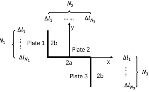
In this section, MoM will be applied to solve a 2D static problem, whose schematic is shown in Fig. 1. The “step” consists of three connected PEC plates, labeled as “1”, “2”, and “3”. Plate 1 and plate 3 are perpendicular to the horizontal plate 2. The thickness of the structure is neglected. The structure carries electric charge, and its surface therefore becomes equipotential with a value of V. The goal is to obtain charge distribution on this structure based on the knowledge of its surface potential, and subsequently, the potential and electric field distribution in the exterior space due to this specific charge distribution.
Figure 1. Schematic for the 2D static problem. The widths of plate 1 and plate 3 are 2b, plate 2 is 2a. There are N1,N2 andN3 subsections on each plate, numbered in the order as shown.
2.1. Construction of Matrix Equation
In an attempt to relate charge distribution and potential, a modified 2D Green’s function Gγ(ρ) = ln(ρ/γ) is used in this paper, instead of the conventional G(ρ) = ln(ρ). The introduced parameter γ
shifts zero potential reference to a designated position, which is preferred to be very far away from the object (though impossible to be true infinity) in order to mimic the 3D conventions (that potential at infinity is 0). The necessity of this modification becomes significant when one is studying electrostatic quantities such as potential and capacitance of large 2D objects. More detailed discussions can be found in Appendix A.
Since the structure is infinitely thin, the surface integral degrades to line integral, and the induced potential φ(r) is determined by:
φ(r) =− 1 2π
LσGγ(ρ)dl
=− 1
2π
Lσln
ρ γdl
(1)
wherer andr are position vectors in observation coordinates and source coordinates;ρ=|r−r|;dl
is the line integral element; σ is the line charge density per unit length; γ is a constant much larger than the dimensions of the object. As will be shown in Appendix A, the choice of γ is not unique, thus a fixed value ofγ must be maintained when comparing electrostatic quantities among different 2D objects.
value V. For this specific geometry, the right-hand side of Eq. (1) can be expanded into three parts, corresponding to the integration on three plates, which leads to the integral equation:
V = −1 2π
2b
0
σ(−a, y) lnρ
γdy
+ −1
2π
a
−aσ(x
,0) lnρ
γdx
+ −1
2π
0
−2bσ(a, y
) lnρ
γdy
(2)
in which ρ=(x−x)2+ (y−y)2.
As shown in Fig. 1, three plates are evenly subdivided into N1, N2, and N3 subsections. Basis function is defined on plate ias pulse function on each subsection:
fni(r) =
1 r ∈Δln
0 r ∈/ Δln i= 1,2,3 n= 1,2, . . . , Ni (3)
The charge densityσ can now be approximated as weighted summations of basis functions:
σ = 3 i=1 Ni n=1
αinfni (4)
with αin being the unknown coefficients to be solved. Substitute Eq. (4) into Eq. (2) and rewrite it in operator representations: 3 i=1 N1 n=1
αinLifni =V (5)
Finally, apply point matching and calculate inner product with weighting functions wjm on both sides of Eq. (5):
3 i=1 N1 n=1
αni wjm, Lifni =wjm, V (6)
with the weighting functions wmj defined on platej as:
wjm =δ(r−rjm) j= 1,2,3 m= 1,2, . . . , Nj (7)
withrjm located at the center of the mth subsection on plate j.
Now, denoting the inner productwmj , Lifni by ljimn, we write Eq. (6) in matrix equation form: ⎡
⎣[l 11
mn] [lmn12 ] [l13mn] [l21mn] [lmn22 ] [l23mn] [l31
mn] [lmn23 ] [l33mn] ⎤ ⎦ ⎡ ⎣[α 1 n] [α2n] [α3
n] ⎤ ⎦=
⎡ ⎣[V
1 m] [Vm2] [V3
m] ⎤
⎦ (8)
in which each block [ljimn] represents anNj×Nimatrix; [αin] represents anNi×1 column vector containing the coefficients αin; [Vmj] represents an Nj×1 column vector with its elements Vmj =wjm, V.
2.2. Diagonal and Off-Diagonal Terms
Before solving Eq. (8), the values oflmnji have to be determined. Recall that:
ljimn=wjm, Lifni = 2−1
π
ln+Δl/2
ln−Δl/2 ln
|rjm−ri|
γ dl
(9)
wherelnis measured from the center of thenth subsection on platei, and Δlis the width of subsection. Notice that for self-patches (diagonal terms,m=nandi=j),ri can be very close to and even overlap withrjm, causing a singularity in the integrand of Eq. (9). However, this integral containing singularity can be evaluated in closed form [10]:
lnnii =−2Δl
πln
Δl
whereeis the Euler’s number approximately equal to 2.7182.
As for the off-diagonal terms, one simple approximation is to assume the logarithmic function to be constant over the entire subsection, and the integral becomes a multiplication:
lmnji ≈ −2Δl
πln
|rjm−rin|
γ i=j, m=n ori=j (11)
in which rin is now located at the center of thenth patch on plate i.
However, sometimes this approximation is too crude to give reliable results, especially in this 2D static scenario. Equation (11) can be very inaccurate for patches that are close to each other, which is more likely to happen when bothrjm and rin are on the same plate. It is advisable to use closed form solution for the integral in these cases [10]:
l22mn = −21
π
tln t
γe
t=|xm−xn|+Δx/2
t=|xm−x
n|−Δx/2
, m=n (12)
liimn = −21
π
tln t
γe
t=|ym−yn|+Δy/2
t=|ym−y
n|−Δy/2
, mi= 1=,n3 (13)
With the results so far, one can determine each element of [lmn] and solve the matrix Equation (8)ji to obtain coefficients αin.
2.3. Potential, Electric Field and Capacitance
With full knowledge of coefficients αin, charge distributionσ can be obtained readily by Eq. (4). With Eq. (1), one is able to obtain the potential at any point r in the space, by substituting the charge by that calculated and approximating the integration in the way as done previously:
φ(r) =− 1 2π
Lσln
ρ γ dl
=− 1
2π L 3 i=1 Ni n=1
αinfni
lnρ
γ dl
≈ − 1
2π 3 i=1 Ni n=1
αinln|r−r i
n|
γ
(14)
Electric field could be obtained using the relation:
E(r) =−∇φ(r) = 1 2π
Lσ∇
lnρ
γ
dl = 1 2π ˆ x· Lσ
x−x
ρ2 dl+ ˆy·
Lσ
y−y ρ2 dl
≈ 1 2π 3 i=1 Ni n=1
αinΔl |r−rin|
(x−xin)ˆx+ (y−yin)ˆy
(15)
whererin =xinxˆ+yinyˆ.
Capacitance for a single object is originally defined as the ratio of total charge to its potential [11]. However, in 2D problems, charge is evaluated per unit length, so will be the capacitance. It is also worth noting that the potential is conventionally measured from zero at infinity, which is not the case if the original 2D Green’s function is used. Only with the modified Green’s function, which creates a zero of potential at “quasi-infinity”, one can conveniently follow the definition above to calculate the capacitance per unit length as:
C= Ql
V = Lσdl V ≈ 1 V 3 i=1 Ni n=1
αinfniΔl
(16)
2.4. Results
2.4.1.
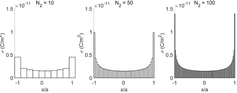
A special case of a= 0.5 m, b = 0 m is first studied, which means that only plate 2 exists. With the potential on the plate set to V = 1 V, charge density is calculated using different numbers (N2) of subsections to manifest the convergence of MoM, whose results are shown in Fig. 2.
Figure 2. For object dimensions of a = 0.5 m, b = 0 m and V = 1 V. Charge density on the object calculated usingN2 = 10, 50, 100.
Singular behavior can be observed near the edge of the plate. As expected, the larger is N2, the better the result will resolve the singular charge distribution near the edge. On the other hand, the charge density in the central area remains at the same level as N2 increases. Overall, N2 > 50 is acceptable.
Potentialφand electric field amplitude|E|distribution in the range of−2a < x, y <2aare plotted in Fig. 3. From the electric field pattern one can easily observe the enhanced electric field resulting from the high charge density at both edges of the plate.
Figure 3. For object dimensions of a = 0.5 m, b = 0 m and V = 1 V. Potential φ and electric field amplitude|E|distribution inx-y plane within −2a < x, y <2a.
The capacitance per unit length of this object is calculated to be 2.28 pF/m.
2.4.2.
Then, a complete “step” with dimensions of a = 0.5 m, b = 0.5 m and a surface potential of
V = 1 V is studied. Here, based on previous results, each plate is divided into 100 subsections, i.e.,
Figure 4. For object dimensions ofa = 0.5 m, b= 0.5 m and V = 1 V. Following the order shown in insets (red arrows), the charge density on plate 1, 2 and 3 is plotted continuously.
to right is plotted continuously in Fig. 4. The three segments separated by red dash lines correspond to charge distributions on plates 1, 2, and 3. Still, one can observe singular charge density at both edges (y =±2b). At the two bends (x=±a), higher charge density occurs but is less singular than that at the edges. Also, on average, plate 1 and plate 3 appear to carry more charge than plate 2.
Potentialφand electric field amplitude|E|distribution in the range of−4a < x, y <4aare plotted in Fig. 5. The electric field pattern reveals the shape of the structure clearly, and the enhanced electric field at edges and bends can be observed.
Figure 5. For object dimensions of a= 0.5 m, b= 0.5 m and V = 1 V. Potential φ and electric field amplitude|E|distribution inx-y plane within −4a < x <4a,−4b < x <4b.
The capacitance of this structure is calculated to be 2.37 pF/m, which is very close to the capacitance of the single plate shown previously. This proximity is reasonable if we compare the charge distribution on single plate (Fig. 2) and that on step-like structure (Fig. 4). Capacitance does not increase as much as the increase of total area of the structure because the overall charge density level drops, and the total charge on the structure does not change as much. As a comparison, the capacitance of a single PEC plate with the same surface area as this step-like structure is also calculated to show the effect of bending. The obtained value is 2.39 pF/m, slightly higher than 2.37 pF/m of the “step”, which implies that folding a 2D planar conductor will reduce its capacitance.
3. 3D STATIC PROBLEM
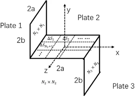
Figure 6. Schematic for the 3D static problem. Plate 1 and plate 3 form right angles with plate 2. The three plates have the same width of 2a in z direction and lengths of 2b, 2a and 2b respectively. There areN1×N1,N2×N2 and N3×N3 subsections on each plate, and are numbered in the order as shown. (only shown for plate 2, plate 1 and plate 3 follow the same rules of numbering).
only that the structure is now finite in z direction, with a width of 2a. Still, the structure has a given potential V, and the goal is to solve its surface charge density, as well as the resulting potential and electric field distribution in the exterior space.
3.1. Construction of Matrix Equation
The construction of matrix equation for 3D problem follows the same routine as discussed for 2D problem. The difference lies in the specific form of integral equation, basis function, and weighting function, thus extra work is required only when it comes to the evaluation of inner products.
Green’s function for 3D static problem is G(R) = 1/R, with R =|r−r|. The potential due to certain charge distributionσ(r) can then be determined by:
φ(r) = 1 4π
σ(r)
R dv
= 1
4π
σ(r)
R ds
(17)
in which volume integral reduces to surface integral because the thickness of the structure is neglected, and therefore σ in this case becomes surface charge density. Following the same procedures done for 2D problem, the integral equation can be constructed for this specific structure as:
V = a
−adz
2b
0 dy
σ(−a, y, z)
4πR +
a
−adz
a −adx
σ(x,0, z)
4πR +
a
−adz
0 −2bdy
σ(a, y, z)
4πR (18)
With the structure divided in the way shown in Fig. 6, pulse function is defined on each subsection of plate ias basis function:
fni(r) =
1 r ∈ΔSn
0 r ∈/ ΔSn i= 1,2,3 n= 1,2, . . . , N 2
i (19)
and the weighting function for point matching is now defined as:
wjm=δ(r−rjm) j= 1,2,3 m= 1,2, . . . , Nj2 (20)
3.2. Diagonal and Off-Diagonal Terms
In general, the inner productljimn takes the form of:
lmnji =wjm, Lifni = 1 4π
ΔSn
1 |rjm−ri|
ds (21)
which includes an integrable singularity for self-patches (diagonal terms, m = n, i = j) that can be evaluated in closed form [1]:
liinn = 0.282 √
An
(22)
whereAnis the area of thenth patch on plate i.
As for off-diagonal terms, it is a good approximation to assume the integrand in Eq. (21) to be constant over each patch, so that:
ljimn= An 4π|rjm−rin|
i=j, m=nori=j (23)
withrin being the center of the nth patch on plate i.
3.3. Potential, Electric Field and Capacitance
With the charge distribution solved by MoM, the induced potential in the entire space can be obtained with Eq. (17), by substituting the charge by calculated and approximating the integration:
φ(r) = 1 4π
⎛ ⎝3
i=1 N2
i
n=1
αinfni ⎞ ⎠ 1 Rds ≈ 1 4π 3 i=1 N2 i n=1
αin An |r−rin|
(24)
The electric field is calculated by:
E =−∇φ(r) =− 1 4π σ∇ 1 R ds
=− 1 4π
ˆ
x·
σ−(x−x
)
R3 ds+ ˆy·
σ−(y−y
)
R3 ds+ ˆz·
σ−(z−z
)
R3 ds ≈ 1 4π 3 i=1 N2 i n=1
αinAn
|r−rin| 3 (x−x i
n)ˆx+ (y−yni)ˆy+ (z−zni)ˆz
(25)
in which rin =xinxˆ+yniyˆ+znizˆ.
The capacitance for this structure can be evaluated in a way similar to Eq. (16).
3.4. Results
3.4.1.
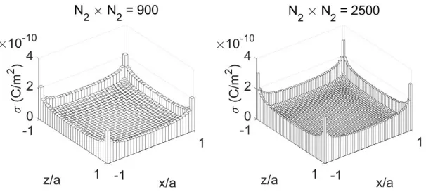
Again, a special case of single plate with a = 0.5 m, b = 0 m, V = 1 V is first studied, whose charge density distribution is calculated using different numbers of subsections, shown in Fig. 7. As expected, charge density appears singular at the edges, especially at the four corners. The finer the subsections are, the better the singular charge distribution will be resolved. However, when Ni increases, the total number of subsections, or equivalently saying, the dimensions of the matrices, will increase as the square ofNi, which costs much more time to compute. For consideration of both computation time and accuracy, N2 = 30, a total number of subsections of 900 is used for following results.
Figure 7. For object dimensions ofa= 0.5 m, b= 0 m and V = 1 V. Charge density calculated using
N2 = 30 and 50.
Figure 8. For object dimensions of a = 0.5 m, b = 0 m and V = 1 V. Potential φ and electric field amplitude|E|distribution in an offsetx-z plane, with offset amount of d= 0.1afrom y= 0 plane.
Since the offsetdis small, the electric field amplitude is still strongly dependent on the local charge density on the structure. A direct relationship between the charge and electric field amplitude can be found from |E| pattern: electric field is the strongest near the corners, less strong at the edges, and weakest at the center, which agrees well with the charge density distribution in Fig. 7.
The capacitance of this structure is calculated to be 40.49 pF.
3.4.2.
Then, a complete “step” witha= 0.5 m, b= 0.5 m, V = 1 V is studied. N1 =N2 =N3 = 30 are used, which means that there are 900 subsections on each plate. The calculated charge distribution on three plates is presented in Fig. 9. Separated by red dash lines, the three segments correspond to charge distributions on plate 1, 2, and 3, from which one can observe singular charge distribution on corners and edges. Charge accumulation can also be found at the bends where adjacent plates are connected.
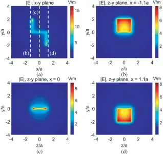
The potential and electric field distribution in x-y plane are very similar to that shown in Fig. 5 for 2D problem and will not be discussed again. Instead, the electric field distributions in a series of cross sections parallel toy-zplane are shown in Figs. 10(b)–(d).
Figure 9. For object dimensions ofa= 0.5 m, b= 0.5 m andV = 1 V. Charge densityσ on each plate is plotted continuously.
(a) (b)
(c) (d)
(b) (c)
(d)
Figure 10. For object dimensions of a = 0.5 m, b = 0.5 m and V = 1 V. (a) |E| distribution in x-y
plane. The white dash lines marks the positions of cross sections taken by (b), (c) and (d). (b) |E|
distribution in x =−1.1a plane. (b)|E|distribution in x= 0 plane. (d) |E| distribution in x = 1.1a
plane.
4. 2D DYNAMIC PROBLEM
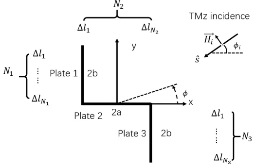
In this section, a 2D dynamic scattering problem will be solved by MoM, whose schematic is shown in Fig. 11. The PEC structure is identical to that used previously for 2D static problem. However, the goal is now to solve the current induced by incident plane wave and then obtain the field scattered by this structure. The incident plane wave forms an angle ofφi withxaxis and is chosen to be TMz polarized, meaning that the electric field is always along z direction. Physical Optics (PO) approximation will also be applied to solve the same problem as a comparison with MoM.
Figure 11. Schematic for the 2D dynamic problem. The widths of plate 1, 2 and 3 are 2b, 2aand 2b. There areN1,N2 and N3 evenly divided subsections on each plate, and are numbered in the order as shown.
4.1. Construction of Matrix Equation
For this kind of thin PEC object, electric field integral equation (EFIE) is typically used [12]:
ˆ
n×Einc= ˆn× 1
4πP.V. jωμ Jψ+
1
jω∇
·J∇ψds (26)
in which ˆn is the surface normal; Einc is the known incident electric field on the surface of the object; the sign P.V.represents principal value integral;Jis the surface current density; andψis the free space Green’s function:
ψ= e− jkR
R , R=|r−r
| (27)
Equation (26) can be simplified for this 2D problem. Based on the fact that Einc and J are z
invariant and have onlyz component under TMz illumination, one could realize that:
∇·J=∇·(ˆzJz) = ∂
∂zJz = 0 (28)
which means that the second term in the integral of Eq. (26) vanishes, and Eq. (26) gets simplified:
ˆ
n×zEˆ zinc= ˆn×zˆ41
πP.V.
(jωμJzψ+ 0)ds⇒Ezinc= 41
π P.V.
(jωμJzψ)ds (29)
The surface integral in Eq. (29) is supposed to perform on a closed surface. However, for this 2D case, this “closed surface” is stretched to±∞ inz direction, meaning that the surface integral can now be treated as a contour integral in x-y plane and a line integral inz direction from −∞to +∞:
Ezinc= 41
π P.V.
CjωμJzdl
+∞ −∞
e−jkR R dz
Notice that the integral taken with respect to z becomes Hankel function of the second kind of order zero [13]:
+∞
−∞
e−jkR R dz
= +∞ −∞
e−jk
√
|ρ−ρ|2+(z−z)2
|ρ−ρ|2+ (z−z)2 dz
= π
jH
(2)
0 (k|ρ−ρ|) (31)
where ρ= ˆxx+ ˆyy,ρ= ˆxx+ ˆyy. The EFIE then reduces to:
Ezinc= kη4 P.V.
CJzH (2)
0 (k|ρ−ρ|)dl (32)
in whichη= 120π is the free space impedance. Equation (32) means that Hankel function of the second kind of order zero is the Green’s function for 2D electrodynamic problem. SinceH0(2)(x) goes to 0 when
xgoes to infinity, it agrees with convention (that field at infinity is zero), and no modification is required as we did for 2D electrostatic case.
Equation (32) can further be expanded into three parts for this specific structure:
Ezinc = kη4 P.V. 2b
0
Jz(−a, y)H0(2)(k|ρ−ρ|)dy+ −a
a Jz(x
,0)H(2)
0 (k|ρ−ρ|)dx
+ 0
−2bJz(a, y
)H(2)
0 (k|ρ−ρ|)dy
(33)
Though integral equations bear different forms in different scenarios, the steps to construct matrix equation are identical. As done for static problems, pulse function is used as basis function so that the induced current Jz can be approximated by weighted summation:
Jz = 3 i=1 Ni n=1
αinfni (34)
in which the coefficients αin are to be solved, and the basis function fni is defined as:
fni(ρ) =
1 ρ ∈Δln
0 ρ ∈/Δln i= 1,2,3 n= 1,2, . . . , Ni (35) Then Eq. (33) can be written into operator form as:
Ezinc= 3 i=1 Ni n=1
αinLifni (36)
Dirac function is used as weighting function in order to perform point matching:
wmj =δ(ρ−ρjm) j= 1,2,3 m= 1,2, . . . , Nj (37) with ρjm being the center of the mth patch on plate j. For both sides of Eq. (33), calculate inner product with wm:j
3 i=1 Ni n=1
αinwjm, Lifni =wjm, Ezinc (38)
With the expression of the incident TMz determined explicitly by:
Ezinc(ρ) =Ezinc(x, y) =E0ejk(xcosφi+ysinφi) (39) whose inner product with weighting function becomes: wjm, Ezinc = Ezinc(ρjm). Finally, denote wjm, Lifni by lmn, and a matrix equation can be constructed from Eq. (38):ji
⎡ ⎣[l
11
mn] [l12mn] [l13mn] [lmn21 ] [l22mn] [l23mn] [l31
mn] [l23mn] [l33mn] ⎤ ⎦ ⎡ ⎣[α 1 n] [α2n] [α3
n] ⎤ ⎦=
⎡ ⎣[E
1 m] [Em2] [E3
m] ⎤
⎦ (40)
4.2. Diagonal and Off-Diagonal Terms
In general, the matrix elementljimn is:
lmnji =wjm, Lifni = kη4
ln+Δl/2
ln−Δl/2 H (2) 0 (k|ρ
j
m−ρi|)dl (41)
wherelnis measured from the center of thenth patch on platei, and the width of this patch is Δl. For self-patches, or say the diagonal terms (i=j,m=n), the Hankel function in Eq. (41) has an integrable singularity, which has a closed form solution [13]:
liinn ≈ βη4 Δln
1−2j
π ln
1.781kΔln 4e
(42)
As for off-diagonal terms, the integral is approximated by:
ljimn≈ βη4 ΔlnH0(2)(k|ρ j
m−ρin| ) i=j, m=nori=j (43)
in which the Hankel function is assumed constant over the patch, with ρin being the center of the nth patch on plate i.
4.3. Physical Optics (PO) Approximation
Apart from MoM, PO is another method to acquire the induced current on the object and yields very good result for large and flat objects. PO assumes the current in shadowed regions on the object to be zero, while approximating the induced current in regions lit by the incident wave as [13]:
JP O= 2ˆn×Hinc (44)
in which Hinc is the incident magnetic field on the surface and can be rewritten under plane wave incidence as:
Hinc= 1
η ˆs×E
inc= 1
η ˆs×zEˆ
inc
z (45)
with ˆsbeing the unit vector in the direction of plane wave propagation: ˆ
s=−cosφixˆ−sinφiyˆ (46) Use expression of Ezinc from Eq. (39), PO current becomes:
JP O(ρ) = 2
ηnˆ×(−sinφixˆ+ cosφiyˆ)E
inc
z (ρ) (47)
Simply picking ρ on the surface of the object and using the correct surface normal ˆn, one can determine the PO current explicitly.
Since the structure under study consists of only thin plates, the determination of lit region is straightforward. However, at certain incident angles one should be careful with extra blockage caused by bending features on this structure.
4.4. Scattered Field
Once induced current J is obtained by either MoM or PO, one can calculate the radiation by this current in order to obtain the scattered field. The scattered field is related to current as [13]:
Es=−kη 4
C
JH0(2)(k|ρ−ρ|)dl (48)
Obviously, the scattered field Es is also in z direction since J has only z component. The large argument approximation of Hankel function can be used since we are interested in the far field behavior of the scattered field, with:
H0(2)(x)≈
2j πxe
−jx
as well as far field approximation for phase term:
e−jk|ρ−ρ|≈e−jkρ·ejkρˆ·ρ, ρ=ρρˆ (50) (48) reduces to:
Es=−zηˆ
jk
8π e−jkρ
√
ρ
CJze jkˆρ·ρ
dl (51)
Finally, substitutingJz by MoM or PO current, one will obtain the scattered field.
4.5. Results
4.5.1.
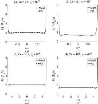
First, the scattering property of a single plate is studied (a= 0, b= 0). The width of the plate (2a) is normalized to wavelength, and two typical values are chosen to compare the performance of MoM and PO at different object dimensions. The subsections are chosen to be λ/10 in width. Normalized currents on the object calculated by MoM and PO, with object dimensions of 2a= 2λ and 2a= 10λ, for two incident anglesφi = 45◦ and 90◦, are plotted in Fig. 12.
Forφi = 90◦ (normal incidence), one could observe that MoM current has singular behavior near the edges, whereas PO does not see the boundary of the structure, and PO current is uniform over the
(a) (b)
(c) (d)
Figure 12. Induced current on single plate calculated by MoM and PO for (a) 2a= 2λ,φi = 90◦. (b) 2a = 2λ, φi = 45◦. (c) 2a = 10λ, φi = 90◦. (d) 2a= 10λ, φi = 45◦. The currents are normalized to
(a)
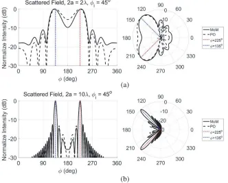
(b)
Figure 13. Normalized scattered far field pattern for normal incidence (φi = 90◦) in Cartesian and polar representation for object dimensions of (a) 2a= 2λ; (b) 2a= 10λ. The blue dash lines mark the direction of reflection while the red dash lines mark the direction of transmission.
(a)
(b)
entire object. However, MoM and PO currents are very close when the observation point is away from the edges. Similar observations can be made forφi = 45◦ (oblique incidence), and only MoM current is now unsymmetric whereas PO current remains uniform. As the structure increases its size, MoM and PO currents show better overall agreement. The corresponding scattered fields are plotted in dB scale, in both Cartesian and polar representations in Figs. 13 and 14.
In both figures, the blue dashed lines highlight the direction of reflection, in which a mainlobe is expected. The red dashed lines stand for the direction of transmission, in which a mainlobe is also expected so as to cancel the incident field when calculating the total field (in the shadow of the object). It can be observed that MoM and PO have very similar predictions of the direction and beamwidth of the mainlobes, but PO appears to give much deeper nulls.
In oblique incidence case, compared with PO, a little deviation in the direction of mainlobe can be observed for MoM, especially when 2a = 2λ. When 2a= 10λ, this difference becomes negligible, and the patterns of MoM and PO agree much better for the entire range of φ.
4.5.2.
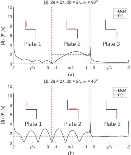
Now, a complete PEC “step” with 2a = 2λ, 2b = 2λ is considered. The induced currents on this structure obtained with MoM and PO are as presented in Fig. 15 for normal and oblique plane wave incidence. From left to right, the currents on plates 1, 2, and 3 are plotted continuously.
Figure 15 reveals huge difference between MoM and PO currents. Under normal incidence (φi = 90◦), as can be expected from Eq. (44), there is no presence of PO current on plates 1 and 3 due to the absence of tangential component of Hinc over them, which leads to an unrealistic sudden
(a)
(b)
Figure 15. Induced current on the structure calculated by MoM and PO for (a) 2a = 2λ, 2b = 2λ,
change of current at the bends. However, MoM does predict non-zero current on plates 1 and 3, and is continuous at the bends.
Under oblique incidence (φi = 45◦), PO current is uniform on each plate, whereas MoM current shows fluctuation around the value of PO current, especially on plates 1 and 2. This fluctuating behavior is a result of mutual effect between plates 1 and 2 (e.g., reflection and diffraction), which is not taken into account by PO. However, MoM current seems flat on plate 3, because under this specific incident angle, the wave hitting plate 3 is simply reflected away and does not further interact with other plates.
Figure 16. The schematic for wedge scattering problem. Incident TMz plane wave forms an angle of
φ with xaxis. The angle of the wedge is 2α.
It is also interesting to look at the current behavior at the bends (marked by red dashed lines in Fig. 15). Unlike charge density σ for 2D static problem that shows singularity at both bends, current densityJ for 2D dynamic problem becomes singular only at the second bend and becomes 0 at the first bend. This phenomenon can be explained by the canonical wedge scattering problem, whose schematic is shown in Fig. 16. The analytical solution of the total electric field under TMz plane wave illumination with an incident angle of φ is [13]:
Et= ˆzE0
v
jvJv(kρ) sin[v(φ−α)] sin[v(φ−α)] (52)
where
v= mπ
2(π−α), m= 1,2,3, . . . (53) Then, according to Maxwell’s equation, the total magnetic field can be determined by:
Ht=− 1
jωμ∇ ×E
t=− 1
jωμ
ˆ
ρ ρ
∂Ezt
∂φ −
ˆ
φ∂E
t z
∂ρ
(54)
Thus the surface current density:
J = ˆn×Ht (55)
Notice that the relation ˆn=±φˆalways holds, which leads to:
J ∝zˆ1
ρ
v
vjvJv(kρ) sin[v(φ−α)] cos[v(φ−α)] (56)
Since we are interested in current behavior near the tip of the wedge (ρ → 0), use the small argument approximation for Bessel function, and Eq. (56) reduces to:
J ∝
v
v(jk/2)v Γ(v+ 1)ρ
v−1sin[
v(φ−α)] cos[v(φ−α)] (57)
which means that currentJ is now a summation of polynomials ofρ, among which the lowest order of
ρ becomes significant, and the higher order terms are negligible when ρ is small. Therefore, only the first term (i.e.,m= 1) in Eq. (57) is considered:
from which one can observe that when α ≥ π/2 (inside corner), the current is proportional to non-negative order of ρ, showing no singularity but goes to 0 near the tip of the wedge; when α < π/2 (outside corner), the current will have a singular behavior near the tip.
Based on the discussions above, one can now explain that the current behavior occurs in Fig. 15. Under these illumination angles (φ= 45◦ or 90◦), plate 1 and plate 2 actually form a wedge that has
α= 3π/4, where the current depends onρ, whereas plate 2 and plate 3 form a wedge that hasα=π/4, where the current depends on ρ−1/3. So, the results agree with what can be expected from Eq. (58) that the current goes to zero at the first bend and becomes singular at the second bend. Following this concept, the edges can be treated as a special case ofα = 0, meaning that the edge current will vary at the order ofρ−1/2. This helps explain why edge current seems more singular than bend current. Note that these current behaviors are related to both the angle of the bend and the incident direction of the plane wave, as stated in [6]. For example, if the plane wave is incident from the other direction, say
φ = 225◦, then the equivalent wedge angles for the two bends will be exchanged. Then, one would expect a singular current at the first bend and a vanished current at the second bend.
The scattered field patterns generated by MoM or PO currents, for object dimensions of 2a= 2λ, 2b = 2λ, under normal and oblique TMz plane wave incidences are presented in Fig. 17. The blue, red, and green dashed lines highlight the direction of reflection by horizontal plate 2, the direction of transmission, and the direction of reflection by vertical plates 1 and 3. In the direction of transmission, two methods agree well, whereas in other directions, the patterns of PO or MoM can be very different.
(a)
(b)
Figure 17. Normalized scattered field pattern for object dimensions of 2a= 2λ, 2b= 2λin Cartesian and polar representations, for (a) normal incidence (φi = 90◦) and (b) oblique incidence (φi = 45◦). The blue, red and green dash lines correspond to direction of reflection by horizontal plate, direction of transmission and direction of reflection by vertical plates. The red and green lines overlap for normal incidence case.
In the direction of reflection by horizontal plate 2 (blue lines), the scattered field is very weak, since most of the reflected energy is then reflected by vertical plate 1, which finally directs the wave back toφ= 45◦ direction. However, in the direction of reflection by vertical plates (green lines), there exists a strong peak, because the wave reflected by vertical plate 3 does not encounter any obstacles. To better illustrate the effect of the vertical plates, a combination of 2a= 2λ, 2b= 4λis also studied, which means that the vertical plates are lengthened. The patterns are shown in Fig. 18.
(a)
(b)
Figure 18. Normalized scattered field pattern for object dimensions of 2a= 2λ, 2b= 4λin Cartesian and polar representations, for (a) normal incidence (φi = 90◦) and (b) oblique incidence (φi = 45◦). The blue, red and green dash lines correspond to direction of reflection by horizontal plate, direction of transmission and direction of reflection by vertical plates. The red and green lines overlap for normal incidence case.
For both normal and oblique incidence cases, one can now observe a stronger scattered field in the right half space and weaker one in the left half. This agrees with intuition since the lengthened vertical plates tend to block more energy transmitting to the left and reflect more energy to the right.
It is worth noting that when dealing with such perfect conducting objects with sharp edges, the accuracy of PO can be improved by the Physical Theory of Diffraction (PTD) [14], which corrects PO current by introducing nonuniform current component. However, the implementation of PTD will not be discussed in this paper for brevity.
5. CONCLUSIONS
Step-like PEC structures, as combinations of several representative canonical geometries, are analyzed with MoM in both electrostatic and electrodynamic scenarios. Unique charge and current behaviors in vicinity of these elemental geometries are revealed by numerical results and validated with the analytical solutions available from corresponding canonical problems.
premise for valid comparison of electrostatic quantities such as potential, electric field, and capacitance among different 2D structures. For both 2D and 3D static cases, charge density distribution under a given surface potential is obtained, whose singular behavior is observed near the edges, corners, and bends on the structures. The potential and electric field in the surrounding space induced by the surface charge are calculated.
In 2D electrodynamic problem, both MoM and PO are utilized to solve induced surface current on a TMz plane wave illuminated PEC step-like structure. In contrast to PO which suggests uniform or discontinuous surface current, MoM reveals fluctuating and continuous surface current. The unique current behavior near the bend region is discussed and explained by modeling each bend as a PEC wedge and resorting to the analytical solution of the canonical wedge scattering problem, which suggests that the appearance of singular current near the bends is determined by the angle of the wedge and the direction of illumination. The scattered far field patterns are also calculated and discussed.
APPENDIX A. MODIFICATION TO 2D STATIC GREEN’S FUNCTION
When dealing with electrostatic potential, it is a convention to choose infinity as a zero potential reference. Since Green’s function is actually the potential induced by a Dirac source, thus setting the potential at infinity to be zero is equivalent to setting the Green’s function to be zero at infinity, which leads to G(R) = 1/R in 3D static case. However, when it comes to 2D static case, the conventionally used Green’s function G(ρ) = lnρ implies that the zero potential reference is now at ρ = 1, instead of ρ = ∞. This special choice of reference not only causes confusion in definition of potential and capacitance (the ratio of charge to potential), but also results in unrealistic charge solutions when solving 2D static problems with MoM.
The problem occurs when the dimensions of the object become large. Consider a single PEC plate, whose width is 2a, and the surface potential is 1 V. Intuitively, an object with a positive potential should carry a positive total charge. However, as shown in Fig. A1, as the width of the plate increases (while keeping the surface potential fixed), the charge distribution turns from positive to negative. This phenomenon is actually embedded in the logarithmic nature of this 2D Green’s function. Recall that the off-diagonal termslmnji for 2D are determined by:
lmnji ≈ −2Δl
πln|r
j
m−rin| (A1)
from which one can observe that whenrjm is very close to rin,lmnji will be positive, indicating that the
nth patch on plate ihas a positive contribution to the potential at point rjm. Asrin moves away from
rjm, at a point when|rjm−ri
n|= 1, this contribution becomes zero. Ifri
n is further away fromrjm, this
contribution will become negative. Obviously, when the dimensions of the object are large enough, it is possible that a pointrjm will receive more negative contribution from remote patches than positive contribution from nearby patches (unlike in 3D, the contribution from remote patches always decays as distance increases). So, overall it will result in an unnatural phenomenon: negative charge can produce positive potential.
This conflict with conventional understanding is actually a result of the choice of zero potential reference, as mentioned previously, and can be resolved numerically by modifying the 2D Green’s function. Inspired by the fact that Green’s function is the response of a Dirac source, the potential of a infinite line charge (point source in 2D) is revisited [11]:
V =− q
2πlnρ+C (A2)
in whichq is the line charge density, andC is a constant. Clearly the zero of potential cannot be chosen conveniently at infinity as this will make C infinite. The original G(ρ) = lnρ indicates that C = 0 is picked for this 2D Green’s function, by doing which the zero of potential is moved to ρ= 1.
In order to maintain a unified definition of potential, it is our goal to set the zero of potential to infinity. Taking advantage of the logarithm function in Eq. (A2), C can be moved inside lnρ and exist as a new constantγ:
V =− q 2πln
ρ
γ (A3)
which changes zero potential reference to ρ=γ, and the corresponding Green’s function becomes:
Gγ(ρ) = ln
ρ γ
(A4)
However, one cannot chooseγto be real infinite, as it will makeGγ(ρ) singular. Instead, by using a finite but large enough γ, the zero of potential is moved to a “quasi-infinity”, which numerically guarantees consistency in definition of 2D electrostatic quantities with 3D conventions.
To determine the acceptable value ofγ, the average chargeσavg on the single PEC plate calculated by MoM is plotted against γ/2a in Fig. A2. By normalizing γ to the maximum width of the plate 2a, average charge densityσavg becomes independent of 2aand can be used as a criterion for convergence. From Fig. A2 one can tell that when the ratioγ/2ais larger than 1010,σavg becomes much less sensitive to γ.
It is worth noting that the introduction of this constantγ is only necessary when there is a need to compare the electrostatic properties among different 2D objects. From Fig. A2, one can conclude that charge becomes a relative quantity since we fix the surface potential while changing the potential reference. It must be emphasized that the discussions over charge, potential, capacitance, and even electric field are only valid under a fixed value ofγ. It is interesting to point out that in some applications
people use 2D static method to analyze strip line structures, in which ground planes are present. The ground plane works as a zero potential reference, and hence by image theory the choice of zero potential reference is automatically saved, due to the ratio in the new Green’s function [9]. Thus, concerning such practical calculations, the original and modified 2D static Green’s function will provide identical results.
REFERENCES
1. Harrington, R. F., Field Computation by Moment Methods, 28–30, Wiley-IEEE Press, 1993. 2. Ney, M. M., “Method of moments as applied to electromagnetic problems,” IEEE Trans. Microw.
Theory Tech., Vol. 33, No. 10, 972–980, Oct. 1985.
3. Kolundzija, B., “Advances in EM modeling of complex and electrically large structures,”
Proceedings of Papers 5th European Conference on Circuits and Systems for Communications (ECCSC’10), 310–320, Belgrade, 2010.
4. Wang, S., X. Guan, X. Ma, D. Wang, and S. Yi, “A fast method of moment to calculate monostatic RCS of arbitrary shaped conducting objects,” 2006 CIE International Conference on Radar, 1–3, Shanghai, 2006.
5. Hanninen, I. and K. Nikoskinen, “Implementation of method of moments for numerical analysis of corrugated surfaces with impedance boundary condition,”IEEE Transactions on Antennas and Propagation, Vol. 56, No. 1, 278–281, Jan. 2008.
6. Ufimtsev, P. Y., B. Khayatian, and Y. Rahmat Samii, “Singular edge behavior: To impose or not impose that is the question,” Microw. Opt. Technol. Lett., Vol. 24, 218–223, 2000.
7. Gong, Z., B. Xiao, G. Zhu, and H. Ke, “Improvements to the hybrid MoM-PO technique for scattering of plane wave by an infinite wedge,”IEEE Transactions on Antennas and Propagation, Vol. 54, No. 1, 251–255, Jan. 2006.
8. Jakobus, U. and F. M. Landstorfer, “Improvement of the PO-MoM hybrid method by accounting for effects of perfectly conducting wedges,”IEEE Transactions on Antennas and Propagation, Vol. 43, No. 10, 1123–1129, Oct. 1995.
9. Harrington, R. F., “Losses on multiconductor transmission lines in multilayered dielectric media,”
IEEE Transactions on Microwave Theory and Techniques, Vol. 32, No. 7, 705–710, Jul. 1984. 10. Bondeson, A., Computational Electromagnetics, 160–161, Springer-Verlag, New York, 2005. 11. Smythe, W. R., Static and Dynamic Electricity, 26–100, Hemisphere Publishing, 1988.
12. Wang, J. J. H., Generalised Moment Methods in Electromagnetics, 173–176, Willey-Interscience, 1991.
13. Balanis, C., Advanced Engineering Electromagnetics, 2nd edition, 644–706, J. Wiley & Sons, Hoboken, 2012.