SWITCHABLE SPLIT-RING FREQUENCY SELECTIVE SURFACES
M. H. B. Ucar, A. Sondas, and Y. E. Erdemli
Electronics and Computer Education Department Kocaeli University, Umuttepe
Kocaeli 41380, Turkey
Abstract—Tunable frequency selective surfaces (FSSs) based on split ring resonators (SRRs) are presented. Tuning performance is achieved by means of several on/off switches placed between the rings of each SRR element. The band-stop FSS response is dynamically tuned to different frequency bands at different switching states. In addition, loadings placed at the corners of outer ring elements, forming a fan-like shape, with additional switches are shown to offer rather fine-tuning capability. A dual-layer FSS is also introduced to demonstrate a filter response over a larger frequency band, and also offers tunable dual-band operation via switching. By using complementary SRR elements, a tunable band-pass response instead can be obtained using a similar switching configuration. Practical switch modeling is also examined in the paper along with the scanning performance of the SRR-FSS. The numerical analysis of the FSS designs is accomplished using a fast periodic array simulator, and the measurements demonstrate preliminary validation of the proposed switching configuration.
1. INTRODUCTION
There has been a significant interest in frequency selective surfaces
(FSSs) since early 1960s. A large body of knowledge and design
techniques exists for FSSs which have been utilized as electromagnetic
filters in a variety of wireless communication applications [1]. An
construction rather easy. Moreover, multiple layers of FSS can increase design flexibility. In this context, multilayer FSS configurations can be employed for use in broad-band or multi-band applications [1–3].
In this paper, we introduce novel FSS designs based on split ring
resonator (SRR) elements. SRR arrays were initially proposed as
metamaterial structures demonstrating µ-negative behavior, yielding band-stop response in a specific frequency band [4]. Recently, SRRs have been employed as FSS elements to provide a similar filter response [5, 6]. Here we consider frequency-tunable FSSs based on SRR elements. Frequency-tuning performance is achieved by means of on/off switches placed between the rings of each SRR element. This switching configuration was originally introduced for a composite left-handed slabwhose band-pass response could be dynamically
tuned to different frequency bands [7]. A similar switching was
also successfully employed in a SRR-based microstrip filter design, providing tunable single-band or dual-band frequency responses [8]. In addition, loadings placed at the corners of outer ring elements, forming a fan-like shape (fan SRR: FSRR), with additional switches is shown to allow for rather fine-tuning operation. A dual-layer SRR (DSRR) arrangement is also presented to demonstrate a filter response over a larger frequency range, and also offers tunable dual-band performance by means of switching. Complementary-SRR (CSRR) elements are as well considered to achieve a tunable band-pass response using a similar switching configuration.
In the paper, we present simulation results to demonstrate multi-frequency performance of the proposed FSS designs, namely, SRR-FSS, FSRR-FSS, DSRR-FSS, and CSRR-FSS. We note that the numerical analysis of the designs is achieved by means of a well-validated periodic array simulator [2, 3, 9]. We also present measured data for SRR-FSS prototypes as a preliminary validation for the proposed switching configuration. While the switches are initially modeled as metallic pads placed between the rings at appropriate locations, simplistic PIN diode and micro-electro-mechanical-system (MEMS) switch models are incorporated into the SRR-FSS design to demonstrate practical switch performance.
2. SWITCHABLE FSS DESIGNS
the periodic array modeled and the structure is presumed to be infinite-periodic in thex-yplane and finite-periodic in thez-dimension. Below we present the transmission characteristics of the proposed FSS designs, namely SRR-FSS, FSRR-FSS, DSRR-FSS, and CSRR-FSS.
2.1. SRR-FSS
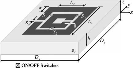
The unit cell configuration of the SRR-FSS design is shown in Fig. 1. The ring resonators are modeled using zero-thickness metallic elements which are supported by a substrate of εr = 3.0 with thickness h =
0.6 mm. The on/off switches (S1,S2,S3) are modeled as metallic pads
(0.3×0.3 mm2) placed along the rings at optimized locations. This switching configuration is similar to the one in [7]. We note that the presence of a metallic pad in a switch location refers to the switch being in on-state, otherwise, in off-state.
h L1
w g
g
S1 S3
S2
L2
x z
y
Dx
Dy
er
ON/OFF Switches
h L1
w g
g
S1 S3
S2
L2
x z
y
Dx
Dy
εr
ON/OFF Switches ON/OFF Switches
Figure1. Unit cell configuration of the SRR-FSS:L1 = 5.7,L2 = 3.3,
g= 0.3,w= 0.9,h= 0.6,Dx=Dy = 7.5 (all in mm),εr= 3.
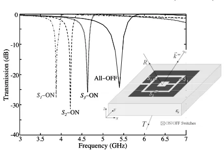
The frequency response of the SRR-FSS is displayed in Fig. 2. As seen, the band-stop response occurs around 5.4 GHz when all of the switches are in off-state (opened). By turning on (closing) each switch at a time, the band-stop response can be tuned to respective frequencies. As seen in Fig. 2, the switch placed equidistant from each of the splits (S2) provides for operation around 4.25 GHz whereas
the switch closer to the split of the outer ring (S1) and the switch
closer to the split of the inner ring (S3) allow for operation at a
lower band (around 3.85 GHz) and at a higher band (around 4.6 GHz), respectively. Hence, the tunable SRR-FSS offers multi-frequency band-stop response over 3.8–5.5 GHz band. In addition, by varying the locations of the switches around the loop between the rings, the corresponding resonant frequencies (fr) can be adjusted to desired
3 3.5 4 4.5 5 5.5 6 6.5 7 -40
-30 -20 -10
Frequency (GHz)
Transmission
(dB)
S1−ON
S2−ON
S3−ON
All−OFF
3 3.5 4 4.5 5 5.5 6 6.5 7
-40 -30 -20 -10
Frequency (GHz)
Transmission
(dB)
S1ON
S2ON
S3ON
All OFF
Figure2. Frequency-tuning performance of the SRR-FSS at normal
incidence (TE-pol,θ=φ= 0◦).
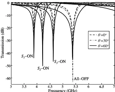
We also examined scanning performance of the SRR-FSS. The related data for TE polarized (TE-pol) incident waves are displayed in Fig. 4. As seen, the band-stop FSS behavior is fairly well maintained for different incidence angles. However, an increase in bandwidth is observed for oblique incidences due to more pronounced magnetic resonance characteristic. On the other hand, for TM polarized (TM-pol) waves, the band-stop response was observed to vanish towards the horizon. In addition, the computed cross-polarization levels were below
−20 dB and−8 dB for the TE-pol and TM-pol cases, respectively, for oblique incidences. This polarization sensitivity, in fact, is expected due to non-symmetrical geometry of the FSS element.
2.2. FSRR-FSS
As discussed above, the switchable SRR-FSS provides tunable
operation with four different bands where each band is apart about 0.5 GHz. In order to offer rather fine-tuning capability, we included metallic loadings at the corners of outer ring elements, forming a fan-like shape (fan SRR: FSRR), and placed additional switches (namely, S4 and S5) along those extensions. The unit cell configuration of the
FSRR-FSS design along with the corresponding frequency response is shown in Fig. 5. As seen, while the switches inserted between the rings (S1/S2/S3) provide coarse tuning (∼0.5 GHz) operation, the switches
placed along the loadings (S4/S5) yield rather fine frequency-tuning
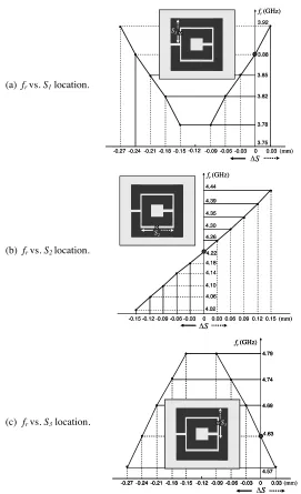
(a) frvs. S1 location.
-0.27 -0.24 -0.21 -0.18 -0.15 -0.12 -0.09 -0.06 -0.03 0 0.03 3.75 3.78 3.82 3.85 3.88 3.92
∆S
S1
fr (GHz)
(mm)
-0.27 -0.24 -0.21 -0.18 -0.15 -0.12 -0.09 -0.06 -0.03 0 0.03 3.75 3.78 3.82 3.85 3.88 3.92
S
S1
fr (GHz)
(mm)
(b) frvs. S2 location.
-0.15 -0.12 -0.09 -0.06 -0.03 0 0.03 0.06 0.09 0.12 0.15 4.02
4.06 4.10 4.14 4.18 4.22 4.30 4.35 4.39 4.44
4.26
∆S
S2
fr (GHz)
(mm)
-0.15 -0.12 -0.09 -0.06 -0.03 0 0.03 0.06 0.09 0.12 0.15 4.02
4.06 4.10 4.14 4.18 4.22 4.30 4.35 4.39 4.44
4.26
S
S2
fr (GHz)
(mm)
(c) frvs. S3 location.
-0.27 -0.24 -0.21 -0.18 -0.15 -0.12 -0.09 -0.06 -0.03 0 0.03 4.57 4.63 4.69 4.74 4.79
∆S
S3
fr (GHz)
(mm)
-0.27 -0.24 -0.21 -0.18 -0.15 -0.12 -0.09 -0.06 -0.03 0 0.03 4.57 4.63 4.69 4.74 4.79
S
S3
fr (GHz)
-0.27 -0.24 -0.21 -0.18 -0.15 -0.12 -0.09 -0.06 -0.03 0 0.03 4.57 4.63 4.69 4.74 4.79
S
S3
fr (GHz)
(mm)
Figure3. Tuning the resonance frequency (fr) of the SRR-FSS design
3 3.5 4 4.5 5 5.5 6 -60 -50 -40 -30 -20 -10 Frequency (GHz) Transm ission (dB )
θ=0o
θ=30o
θ=60o
S1−ON
S2−ON
S3−ON
All−OFF
3 3.5 4 4.5 5 5.5 6 6.5
-60 -50 -40 -30 -20 -10 Frequency (GHz) Transm ission (dB )
θ=0o
θ=30o
θ=60o
θ=0o
θ=30o
θ=60o
S1 ON
S2 ON
S3 ON
All OFF
7
Figure4. Scanning performance of the tunable SRR-FSS design
(TE-pol,φ= 0◦).
3 3.5 4 4.5 5 5.5 6 6.5 7
-60 -50 -40 Frequency (GHz) Transmission (dB)
S4 /S5−OFF
S4−ON, S5−OFF
S4 /S5−ON
S1
S4
S5
S4
S5
S4 S5
S4 S5 S3 S2 Dx Dy k S1 S4 S5 S4 S5
S4 S5
S4 S5 S3 S2 Dx Dy k -30 -20 -10 0
S1−ON
S2−ON
S3−ON
All−OFF
3 3.5 4 4.5 5 5.5 6 6.5 7
-60 -50 -40 Frequency (GHz) Transmission (dB)
S4 /S5OFF
S4ON, S5OFF
S4 /S5ON
S4 /S5OFF
S4ON, S5OFF
S4 /S5ON
S1
S4
S5
S4
S5
S4 S5
S4 S5 S3 S2 Dx Dy k S1 S4 S5 S4 S5
S4 S5
S4 S5 S3 S2 Dx Dy k -30 -20 -10 0
S1ON
S2ON
S3ON
All OFF
Figure5. Frequency-tuning performance of the FSRR-FSS at normal
incidence (TE-pol,θ=φ= 0◦). Dx =Dy = 9.9 mm and k= 0.6 mm;
all other parameters are same as those of the SRR-FSS design (see Fig. 1).
2.3. DSRR-FSS
in Fig. 6. Each layer (Layer-1/Layer-2) was designed individually to provide a band-stop response at 4.6 GHz and 5.4 GHz, respectively. In fact, the layer designated as Layer-1 is same as the SRR-FSS design (see Fig. 1) in absence of switches. The unit cell (Dx, Dy) and ring
dimensions of Layer-2 (w,L1,L2) were chosen to be almost 1.25 times
those of Layer-1. Since the layers now have different periodicities, the dual-layer configuration is referred to as non-commensurate and such a structure is analyzed via the periodic array simulator in an
approximate manner [2]. By placing these layers in cascade, we
optimized the distance between the layers to achieve a wider rejection band centered around 5.2 GHz as seen in Fig. 6. Furthermore, we considered a switched DSRR-FSS configuration, yielding a tunable dual-band filter response as displayed in Fig. 7. As shown, for each layer, there is one switch (S1,i, i = 1, 2) placed between the rings
nearby each outer split. When the switch on Layer-1 (S1,1) is closed
with the switch on Layer-2 (S1,2) opened, the DSRR-FSS results in a
dual-band rejection response around 3.8 GHz and 5.15 GHz. When the switch positions are reversed, the dual-band response shifts to about 3.65 GHz and 5.3 GHz, respectively; that is, the rejection bands are further separated.
3 3.5 4 4.5 5 5.5 6 6.5 7
-50 -40 -30 -20 -10 0
Frequency (GHz)
Trans
m
is
si
o
n
(
dB)
Dual-Layer Layer-1 Layer-2
Layer-1
Layer-2
0.9 mm
3 3.5 4 4.5 5 5.5 6 6.5 7
-50 -40 -30 -20 -10 0
Frequency (GHz)
Trans
m
is
si
o
n
(
dB)
Dual-Layer Layer-1 Layer-2
Layer-1
Layer-2
3 3.5 4 4.5 5 5.5 6 6.5 7
-50 -40 -30 -20 -10 0
Frequency (GHz)
Trans
m
is
si
o
n
(
dB)
Dual-Layer Layer-1 Layer-2
Layer-1
Layer-2
0.9 mm
Figure6. Transmission characteristics of the DSRR-FSS at normal
incidence (TE-pol,θ=φ= 0◦).
2.4. CSRR-FSS
3.5 4 4.5 5 5.5 6 6.5 7 -50
-40 -30 -20 -10
Transm
ission
(dB)
S1,1−ON, S1,2−OFF
S1,1−OFF, S1,2−ON
Frequency (GHz)
3 -60
Layer-1
Layer-2 S1,1
S1,2
3.5 4 4.5 5 5.5 6 6.5 7
-50 -40 -30 -20 -10
Transm
ission
(dB)
S1,1ON, S1,2OFF
S1,1OFF, S1,2ON
Frequency (GHz)
3 -60
Layer-1
Layer-2 S1,1
S1,2
Figure7. Transmission characteristics of the tunable DSRR-FSS at
normal incidence (TE-pol,θ=φ= 0◦).
S1−ON
S2−ON
All−OFF
3 3.5 4 4.5 5 5.5 6 6.5 7
-60 -50 -40 -30 -20 -10 0
Frequency (GHz)
Transmission (dB
)
S3−ON
S1 S3
S2
S1 S3
S2 S1ON
S2 ON
All OFF
3 3.5 4 4.5 5 5.5 6 6.5 7
-60 -50 -40 -30 -20 -10 0
Frequency (GHz)
Transmission (dB
)
S3ON
S1 S3
S2
S1 S3
S2
Figure8. Frequency-tuning performance of the switchable
CSRR-FSS at normal incidence (TM-pol, θ=φ= 0◦).
switchesS1,S2, andS3 allow for operation around 4.25 GHz, 4.7 GHz,
and 5.25 GHz, respectively. Thus, the tunable CSRR-FSS offers multi-frequency band-pass response over 4.0–6.5 GHz band. We remark that while the SRR-FSS offers a band-stop response for the TE-pol case, the CSRR-FSS provides a band-pass response for the TM-pol case, an expected behavior of such complementary structures.
3. MEASUREMENTS
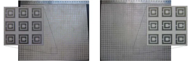
In order to validate the proposed switching configuration for the SRR-FSS design (see Fig. 1), two SRR-FSS panels were fabricated and free-space transmission measurements were carried out. One of the panels consists of SRR elements with no metallic pads, referring to all switches being in off-state, while the other one includes pads in S3 switch
locations only (that is,S3-ON andS1/S2-OFF) as displayed in Fig. 9.
Each panel consists of 37×30 metallic SRR elements (overall size: 27.8×22.8 cm2) etched on an RO3003 substrate with dielectric constant of εr = 3.0 ±0.04 (tanδ = 0.0013) and thickness h = 0.0508 cm
(0.02 inch). The corresponding measurements were carried out using the setup comprised of two standard-gain horn antennas (1–18 GHz,
ETS-Lindgren Model-3115) and AgilentTM E8362B PNA network
analyzer as shown in Fig. 10. The measured and related simulated data are displayed in Fig. 11. As seen, the responses of the finite-size FSS panels are predicted fairly well by the simulated infinite-size SRR-FSS designs with a slight downward frequency-shift of about 0.25 GHz. More importantly, the frequency-tuning performance is demonstrated with this preliminary realization.
Figure9. Fabricated SRR-FSS panels without (left) and with (right)
metallic pads (inS3 switch locations).
Figure10. Setup used for transmission measurements of the SRR-FSS panels.
4 4.5 5 5.5
-30 -25 -20 -15 -10 -5 0
Frequency (GHz)
Transmission
(dB)
S3−ON
(w/ metallic pads)
S1/S2/S3−OFF (w/o metallic pads) Measurements
Simulations
4 4.5 5 5.5 6.5
-30 -25 -20 -15 -10 -5 0
Frequency (GHz)
Transmission
(dB)
S3 ON
(w/ metallic pads)
S1/S2/S3 OFF (w/o metallic pads) Measurements
Simulations Measurements Simulations
6
Figure11. Simulated and measured transmission responses of the
SRR-FSS designs.
the previous simulated FSS responses (Fig. 2) have about 0.25 GHz lower resonant frequencies as compared to the current simulation results (Fig. 11). There are several reasons for those differences. The substrate thicknesshoriginally was 0.06 cm, but the fabricated panels
had h=0.0508 cm, with which the SRR-FSS was then re-modeled.
Also, while re-meshing the structure in the simulator, two prism layers were used instead of just one for a more accurate modeling
of the substrate. Those two changes applied in the simulations
metallic thicknesses of 35µm along with the designated tolerance values forεrwere considered in the re-modeling, an additional 0.05 GHz
upward frequency-shift was achieved in the responses, thus resulting in optimum agreement between the measured and predicted data
as seen in Fig. 11. We also note that more sensitive far-field
measurements with larger FSS panels would yield better agreement with the simulations.
4. ACTUAL SWITCH MODELING
For practical implementation of the switchable SRR-FSS designs, surface-mounted PIN diode or MEMS switches would be the preferred choice due to their compact, low-loss and high-isolation features [10, 11]. To demonstrate possible effects of practical switches on the FSS performance, we included simple equivalent models for the switches (in lieu of metallic pads) in the analysis and the corresponding simulations carried out as discussed below.
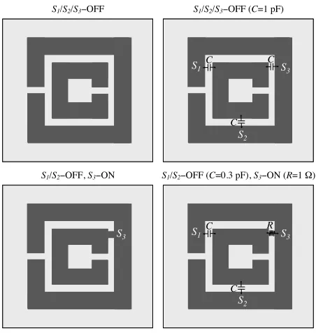
4.1. Pin DiodeModeling
In PIN diode modeling, the switches were modeled as capacitors (C = 0.3−1 pF) and resistors (R = 1 Ω) when they are in off-state and in on-state, respectively, as displayed in Fig. 12. Those capacitor and resistor values represent actual switch behavior in an approximate manner. A representative FSS performance with the switch model is shown in Fig. 13. As seen, by the inclusion of the switch model, there is almost no effect observed in the response when all switches are in off-state. However, the frequency response is shifted downward slightly (∼0.1 GHz) and the corresponding suppression levels increase somewhat for the case only S3 switch in on-state as compared to the
response of the metallic-pad modeling. These differences, in fact, are expected and demonstrate tolerable switch effects in a practical implementation.
4.2. MEMS Switch Modeling
In MEMS switch modeling, the switches were modeled as two-legged bridges based on cantilever MEMS switch structure [12] as depicted in Fig. 14. As seen, this simplistic model consists of a resistive card (RcΩ/cm2) placed on two metal legs where Rc represents possible
S1 S3
S2
C . C. C
. .
.
.
S1 S3
S2
C . C. C
. .
.
.
S1/S2−OFF, S3−ON S1/S2−OFF (C=0.3 pF), S3−ON (R=1 Ω)
S3
S3 S1 S3
S2
C . R.
.
C
. .
.
S1 S3
S2
C . R.
.
C
. .
.
Figure12. Metallic-pad modeling (left column) and equivalent
PIN-diode modeling (right column) of the switches in the SRR-FSS design.
4 4.2 4.4 4.6 4.8 5 5.2 5.4 5.6 5.8 6
-30 -20 -10 0
Frequency (GHz)
Trans
m
ission
(dB)
Metallic pad PIN diode
S1/S2−OFF
S3−ON
S1/S2/S3−OFF
4 4.2 4.4 4.6 4.8 5 5.2 5.4 5.6 5.8 6
-30 -20 -10 0
Frequency (GHz)
Trans
m
ission
(dB)
Metallic pad PIN diode Metallic pad PIN diode
S1/S2 OFF
S3 ON
S1/S2/S3 OFF
Figure13. Effects of PIN-diode equivalent circuit modeling on the
S3
S1
S2
S3
S1
ON OFF
hb
Rc
S3
S1
S2
S3
S1
ON OFF
hb
Rc
Figure14. MEMS switch modeling in the SRR-FSS design (the
modeling forS1/S2-OFF,S3-ON is shown).
4.2 4.4 4.6 4.8 5 5.2 5.4 5.6 5.8
-30 -20 -10 0
Frequency (GHz)
Trans
m
ission
(dB)
S1/S2−OFF
S3−ON
(2) (3)
Metallic-pad modeling MEMS-bridge modeling
S1/S2/S3−OFF
(1) (5)
(6)
(4)
4.2 4.4 4.6 4.8 5 5.2 5.4 5.6
-30 -20 -10 0
Frequency (GHz)
Trans
m
ission
(dB)
S1/S2 OFF
S3 ON
(2) (3)
Metallic-pad modeling MEMS-bridge modeling Metallic-pad modeling MEMS-bridge modeling
S1/S2/S3 OFF
(1) (5)
(6)
(4)
6
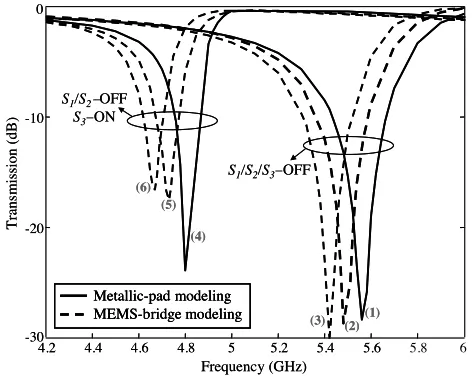
Figure15. Effects of MEMS-bridge modeling on the SRR-FSS
performance. Simulations for metallic-pad modeling (1 & 4) and MEMS modeling (see Fig. 14) for (2) hb = 0.1 mm, (3) hb = 0.05 mm,
(5) hb = 0.1 mm, Rc = 1 Ω and (6) hb = 0.05 mm, Rc = 0.5 Ω are
displayed.
designs with MEMS switch models are displayed in Fig. 15. As seen, by the inclusion of the switch model, the responses are shifted downward slightly (0.05–0.1 GHz) for both switching states (i.e., all in off-state and only S3 on-state) due to expected capacitive loading imposed by
for the latter switching state due to loss introduced by the resistive
cards. In brief, MEMS switch modeling demonstrates acceptable
switch performance in an actual implementation.
5. CONCLUSION
In the paper, tunable FSS designs using SRR elements along with on/off switches have been introduced. The corresponding simulations supported by measurements demonstrated that the band-stop filter response for the switchable SRR-FSS design could be dynamically tuned to different frequency bands over the frequency band of interest. In addition, it was shown numerically that the use of actual switches would have a minimal effect on the FSS performance. Polarization and incidence angle sensitivity of the SRR-FSS were also examined. In addition, switchable fan-like FSRR-FSS design was shown to
provide rather fine-tuning capability. The SRR-FSS design was
extended to include multiple FSS layers (namely, DSRR-FSS), offering
larger bandwidth and dual-band performance via switching. The
complementary version of the design (CSRR-FSS) was also presented,
providing tunable band-pass filter response. To conclude, novel
switchable FSS designs are proposed in the paper with noting that implementation difficulties, such as mounting and biasing of the switches, should be assessed in realization.
ACKNOWLEDGMENT
We would like to thank Dr. Fatih Ustuner from The Scientific and Technological Research Council of Turkey (TUBITAK) for his assistance during the fabrication and measurements of the FSS prototypes.
REFERENCES
1. Munk, B. A., Frequency Selective Surfaces: Theory and Design, John Wiley & Sons, New York, 2000.
2. Erdemli, Y. E., K. Sertel, R. A. Gilbert, D. E. Wright, and J. L. Volakis, “Frequency-selective surfaces to enhance performance of broad-band reconfigurable arrays,” IEEE Trans. Antennas Propagat., Vol. 50, No. 12, 1716–1724, 2002.
IEEE Trans. Antennas Propagat., Vol. 52, No. 11, 2860–2870, 2004.
4. Pendry, J. B., A. J. Holden, D. J. Robins, and W. J. Stewart, “Magnetism from conductors and enhanced nonlinear phenom-ena,” IEEE Trans. Microwave Theory Tech., Vol. 47, No. 11, 2075–2084, 1999.
5. Beruete, M., R. Marques, J. D. Baena, and M. Sorolla, “Resonance and cross-polarization effects in conventional and complementary split ring resonators periodic screens,” Proc. IEEE Antennas Propagat. Soc. Int. Symp., 794–797, Washington D.C., July 3–8, 2005.
6. Bardi, I., R. Remski, D. Perry, and Z. Cendes, “Plane wave scattering from frequency-selective surfaces by the finite-element method,”IEEE Trans. Magnetics, Vol. 38, No. 2, 641–644, 2002. 7. Erdemli, Y. E. and A. Sondas, “Dual-polarized frequency-tunable composite left-handed slab,” Journal of Electromagnetic Waves and Applications, Vol. 19, No. 14, 1907–1918, 2005.
8. Cenk, C., A. Sondas, and Y. E. Erdemli, “Tunable split ring resonator microstrip filter design,” Proc. Mediterranean Microwave Symposium, 20–23, Genova, Italy, Sep. 19–21, 2006. 9. Eibert, T. F., Y. E. Erdemli, and J. L. Volakis, “Hybrid
finite element-fast spectral domain multilayer boundary integral modeling of doubly periodic structures,” IEEE Trans. Antennas Propagat., Vol. 51, No. 9, 2517–2520, 2003.
10. Chang, T. K., R. J. Langley, and E. A.Parker, “Active frequency-selective surfaces,”IEE Proc-Microw. Antennas Propag., Vol. 143, No. 1, 62–66, 1996.
11. Schoenlineer, B., A. Abbaspour-Tamijani, L. C. Kempel,
and G. M. Rebeiz, “Switchable low-loss RF MEMS Ka-band
frequency-selective surface,” IEEE Trans. Microwave Theory
Tech., Vol. 52, No. 11, 2474–2481, 2004.