ANALYSIS OF A GAP-COUPLED STACKED ANNULAR RING MICROSTRIP ANTENNA
J. A. Ansari, R. B. Ram, and P. Singh
Department of Electronics and Communication University of Allahabad
Allahabad 211002, India
Abstract—A theoretical analysis of a gap-coupled stacked annular
ringmicrostrip antenna with superstrate is performed in order to obtain wider bandwidth operation. The effects of air gap, superstrate thickness and feedingpoint location on the antenna performance
are analyzed in TM11 mode usingequivalent circuit concept. It is
noted that the proposed antenna is very sensitive to the feedingpoint
location in TM11 mode while annular ringmicrostrip patch antenna
is independent of feed point in that mode. The optimized proposed antenna shows an impedance bandwidth of 13.96% whereas the antenna without air-gap has 8.75% bandwidth and without superstrate it has bandwidth of 10.89%. The theoretical results are compared with simulated and experimental results.
1. INTRODUCTION
Microstrip patch antennas are becomingpopular because of their
numerous advantages such as their low profile, conformability,
low fabrication cost, mechanical robustness, polarization agility, compatibility/easy integration with microstrip circuits/solid state
devices and adaptability to active antenna elements. Although, in
principle, the patch may be of any shape yet, in practice, only simple geometries like rectangular, square and circular structures
are commonly employed. Like rectangular and circular patches,
Therefore, a number of bandwidth extension techniques have been suggested to achieve better performance of the ARMSA including use of thick substrate [2], use of air gap [3], use of superstrate [4], use of parasitic elements [5–7] and integration of active devices [8]. Amongthese techniques, the stacked parasitic configuration has been selected because it provides close spacingbetween the elements that is not realized in single layer parasitic elements, it does not excite surface waves that occur in thick dielectric substrate, and it does not generate high order modes that are generated for low dielectric substrate [7]. In this paper, the theoretical investigation of a gap-coupled stacked annular ringmicrostrip antenna is presented in which foam material introduces an air gap between the fed and parasitic patches. The results obtained are compared with simulated (IE3D) and experimental [5] results.
2. ANTENNA DESIGN AND THEORETICAL CONSIDERATIONS
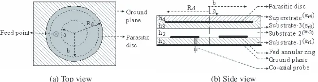
The geometrical configuration of the proposed antenna is shown in Fig. 1. It consists of a probe fed annular ring and a parasitic circular
disc. The inner and outer radii of the ringare a = 8.81 mm and
b = 21.2 mm, respectively. The radius of the disc (Rd = 24.39 mm)
is taken slightly greater than the outer radius of the ring to impose a different but close resonance frequency to the resonance frequency of the ring. The fed and parasitic patches are etched on a dielectric
substrate of relative dielectric constant εr1 =εr3 = 2.2 and thickness
h1 = h3 = 1.59 mm. A foam substrate of relative permittivity
εr2 = 1.06 and thickness h2 = 3.18 mm has been introduced between
the two patches to provide air gap-coupling between them when the fed patch is excited by a 50 ohm coaxial probe of radius 1.25 mm. The probe is located very close to the inner radius of the ringsuch that
its distance from the center of the ringis Y0 = 9.45 mm. Moreover,
(a) Top view (b) Side view
a superstrate of relative dielectric constant εr4 = 2.2 and thickness
h4 = 3.18 mm covers the parasitic patch to protect the antenna from
environmental hazards. The bottom patch is so designed that it can operate at 2.30 GHz.
Due to the presence of the parasitic patch, the proposed stacked structure behaves as an antenna havingtwo resonance frequencies. One resonance frequency is associated with the resonator formed by the fed annular ringand second one is associated with the resonator formed by the parasitic disc. Due to the presence of superstrate the effective dielectric constant for the two resonators are changed causing change in their resonance behaviors. The dielectric substrate in three layers above the annular ringcan be considered as a superstrate of relative
dielectric constantεrs that can be given as [9]
εrs=
4
i=2
hi
4
i=2
hi
eri
(1)
Therefore, the effective dielectric constant for the first resonator is given as [10]
εef =εr1q1+εrs
(1−q1)2
εrs(1−q1−q2) +q2
(2)
whereq1 and q2 are the fillingfactors defined as [10].
The effective dielectric constant with superstrate can be
represented as a single patch with semi-infinite superstrate with relative dielectric constant equal to unity and a single relative dielectric
constant equal toεrf which is given as [10]
εrf =
2εef −1 +Af
1 +Af
(3)
whereAf =
1 +12h1
w
−1/2
;w=b−a.
Therefore, the resonance frequency of the first resonator is given as
ff nm =
Xnmc
2πa√εef
(4)
whereXnmis themth zero ofJn (2Xnm)Yn(Xnm)−Jn (Xnm)Yn(2Xnm)
In the similar fashion, the equivalent relative dielectric constant of the all three layers of the substrate below the parasitic disc can be given as
εrd=
3
i=1
hi
3
i=1
hi
eri
(5)
The effective dielectric constant for the second resonator with the superstrate can be given as
εed =εrdq1 +εr4
(1−q1)2
εr4(1−q1−q2) +q2
(6)
whereq1 and q2 are the fillingfactors for the parasitic patch.
Therefore, the resonance frequency of the second resonator is given as
fdnm =
xnmc
2πRde√εed
(7)
wherexnm is the mth zero of Jn(kRd) and xnm =kRd; k is the wave
number in the dielectric medium. The effective radius Rde of the disc
is given as [11]
Rde=Rd
1+2 (h1+h2+h3)
πRdεed
log πRd
2 (h1+h2+h3)+1.7726
1/2 (8)
The equivalent circuit of the first and second resonators, based on modal expansion cavity model [12], is shown in Figs. 2(a) and (b) from which their impedances can be derived as
ZANNULAR =
jωL1R1
R1−ω2L1C1R1+jωL1 (9)
and
ZDISC =
jωL2R2
R2−ω2L2C2R2+jωL2 (10)
The resistance R1, inductance L1 and capacitance C1 of the annular
ringare calculated as [8]. R2,L2andC2 are the resistance, inductance
(a) (b)
(c)
Figure 2. (a) Equivalent circuit of first resonator, (b) Equivalent
circuit of second resonator, (c) Equivalent circuit of the proposed antenna.
If cp be the couplingfactor, the mutual inductance LM and mutual
capacitanceCM are given as
LM =
c2
p(L1+L2) + c4p(L1+L2)2+ 4c2p
1−c2
p
L1L2
21−c2
p
(11)
CM =
−(C1+C2) + (C1+C2)2−C1C2
1− c12
p
2 (12)
The equivalent circuit of the proposed antenna is shown in Fig. 2(c). From this figure, the impedance of the proposed antenna can be derived as
Zin =jω LP +
ω2RTL2T +jωRT2LT
1−ω2LTCT
ω2ω2R2
TL2TCT2 −2RT2LTCT +L2T
+R2T (13)
where RT = RR11+RR22, LT = LL11+LL22, CT = (CC11++CC22+)CCMM and LP is the
The return loss (RL) of the antenna is given as
RL= 20 log10|Γ|, Γ = (Zin−Z0)/(Zin+Z0) (14)
whereZ0 is the characteristic impedance of the feedingline (50 ohm).
As there exists electromagnetic coupling between the fed patch and the parasitic patch, the radiation from the proposed antenna is contributed by the couplingbetween them. Therefore, for the far-field radiation of the proposed antenna, followingassumptions can be made.
1. The slot voltage induced in the parasitic patch iscp times the slot
voltage of the fed patch.
2. The radiations from the two patches can be considered to be in the same phase because the gap between the fed patch and the parasitic patch are very small as compared to the far-field point. Hence the radiated far-field of the proposed antenna can be given as
Eθ = EθANNULAR+EθDISC (15)
Eφ = EφANNULAR+EφDISC (16)
where the radiation field for fed annular patch are given as [10]
EθANNULAR = j
n2hk
0E0
π knm
e−jkor
r
Jn (k0asinθ)
−Jn (k0bsinθ)
Jn (knma)
Jn (knmb)
cosnφ (17)
EφANNULAR = −j
n2nhk0E0
π knm
e−jkor
r
Jn(k0asinθ)
k0asinθ
−Jn(k0bsinθ)
k0bsinθ
Jn (knma)
Jn (knmb)
cosθ·sinnφ (18)
and the radiation field for the parasitic disc are given as [11]
EDISCθ = j
nk0R dcpV0
2
e−jk0r
r [Jn+1(k0Rdsinθ)
−Jn−1(k0Rdsinθ)] cosnφ (19)
EDISCφ = j
nk0R dcpV0
2
e−jk0r
r [Jn+1(k0Rdsinθ)
+Jn−1(k0Rdsinθ)] cosθ·sinnφ (20)
where V0 = hE0Jn(kRd) is the radiating edge voltage, and r is the
distance of an arbitrary far-field point. k0 andknmare the propagation
constant in free space and dielectric medium respectively in TMnm
3. CALCULATIONS AND DISCUSSION OF RESULTS
The calculations of return loss for different parameters were accomplished usingEquation (14); the resultingdata are shown in Figs. 3–6. Fig. 3 shows the variation of return loss with frequency at
2 2.1 2.2 2.3 2.4 2.5 2.6 2.7 2.8 2.9 3
-30 -25 -20 -15 -10 -5 0 Frequency (GHz) h2=0.00 mm h2=1.59 mm h2=3.18 mm h2=4.77 mm h2=6.36 mm
Return loss (dB)
− − − − − − − − − − − − − − − − − − − − − − − − − − − − − − − − − − − − − − − − − − − − − − − − − − − − − − − − − − − − − − − − − − − − − − − − − − − − − − − − − − − − − − − − − − − − − − − − − − − − − − − − − − − − − − − − − − − − − − − − − − − − − − − − − − − − − − − − − − − − − − − − − − − − − − − − − − − − − − − − − − − − − − − − − − − − − − − − − − − − − − − − − − − − − − − − − − − − − − − − − − − − − − − − − − − − − − − − − − − − − − − − − − − − − − − − − − − − − − − − − − − − − − − − − − − − − − − − − − − − − − − − − − − − − − − − − − − − − − − − − − − − − − − − − − − − − − − − − − − − − − − − − − − − − − − − − − − − −− − − − − − − − − − − − − − − − − − − − − − − − − − − − − − − − − − − − − − − − − − − − − − − − − − − − − − − − − − − − − − − − − − − − − − − − − − − − − − − − − − − − − − − −− − − − − − − − − − − − − − − − − − − − − − − − − − − − − − − − − − − − − − − − − − − − − − − − − − − − − − − − − − − − − − − − − − − − − − − − − − − − − − − − − − − − − − − −− − − − − − − − − − − − − − − − − − − − − − − − − − − − − − − − − − − − − − − − − − − − − − − − − − − − − − − − − − − − − − − − − − − − − − − − − − − − − − − − − − − − − − − −− − − − − − − − − − − − − − − − − − − − − − − − − − − − − − − − − − − − − − − − − − − − − − − − −− − − − − − − − − − − − − − − − − − − − − − − − − − − − − − − − − − − − − − − − − − − − − − − − − − − − − − − − − − − − − − − − − − − − − − − − − − − − − − − − − − − − − − − − − − − − − − − − − − − − − − − − − − − − − − − − − − − −− − − − − − − − − − − − − − − − − − − − − − − − − − − − − − − − − − − − − − − − − − − − − − − − − − − − − − − − − − − − − − − − − − − − − − − − − − − − − − − − − − − − − − − − − − − − − − − − −− − − − − − − − − − − − − − − − − − − − − − − − − − − − − − − − − − − − − − − − − − − − − − − − − − − − − − − − − − − − − − − − − − − − − − − − − − − − − − − − − − − − − − − −− − − −
Figure 3. Variation of return loss with frequency at different air-gap
spacing(h2).
2 2.1 2.2 2.3 2.4 2.5 2.6 2.7 2.8 2.9 3
-30 -25 -20 -15 -10 -5 0 Frequency (GHz) h4=0.00 mm h4=0.79 mm h4=1.59 mm h4=3.18 mm
Return loss (dB)
− − − − − − − − − − − − − − − − − − − − − − − − − − − − − − − − − − − − − − − − − − − − − − − − − − − − − − − − − − − − − − − − − − − − − − − − − − − − − − − − − − − −− − − − − − − − − − − − − − − − − − − − − − − − − − − − − − − − − − − − − − − − − − − − − − − − − − − − − − − − − − − − − − − − − − − − − − − − − − − − − − − − − − − − − − − −− − − − − − − − − − − − − − − − − − − − − − − − − − − − − − − − − − − − − − − − − − − − − − − − − − − − − − − − − − − − − − − − − − − − − − − − − − − − − − − − − − − − − − − −− − − − − − − − − − − − − − − − − − − − − − − − − − − − − − − − − − − − − − − − − − − − − − − − − − − − − − − − − − − − − − − − − − − − − − − − − − − − − − − − − − − − − − − −− − − − − − − − −− − − − − − − − − − − − − − − − − − − − − − − − − − − − − − − − − − − − − − − − − − − − − − − − − − − − − − − − − − − − − − − − − − − − − − − − − − − − − − − − − − − − − − − − −− − − − − − − − − − − − − − − − − − − − − − − − − − − − − − − − − − − − − − − − − − − − − − − − − − − − − − − − − − − − − − − − − − − − − − − − − − − − − − − − − − − − − − − −− − − − − − − − − − − − − − − − − − − − − − − − − − − − − − − − − − − − − − − − − − − − − − − − − − − − − − − − − − − − − − − − − − − − − − − − − − − − − − − − − − − − − − − −− − − − − − − − − − − − − − − − − − − − − − − − − − − − − − − − − − − − − − − − − − − − − − − − − − − − − − − − − − − − − − − − − − − − − − − − − − − − − − − − − − − − − − − −− − − − − − − − − − − − − − − − − − − − − − − − − − − − − − − − − − − − − − − − − − − − − − − − − − − − − − − − − − − − − − − − − − − − − − − − − − − − − − − − − − − − − − − − − − − − − − − − − − − − − − − − − − − − − − − − −− − − − − − − − − − − − − − − − − − − − − − − − − − − − − − − − − − − − − − − − − − − − − − − − − − − − − − − − − − − − − − − − − − − − − − − − − − − − − − − − − − − − − − − − − − − − − − − −− − − − − − − − − − − − − − − − − − − − − − − − − − − − − − − − − − − − − − − − − − − − − − − − − − − − − − − − − − − − − − − − − − − − − − − − − − − − − − − − − − − − − − − − − − − − − − − − − − − − − − − − − − − − − − − − − − − − − − − − − − − − − − −− − − −
Figure 4. Variation of return loss with frequency at different
different air-gap spacing (h2). It is observed that in the absence of air-gap, the antenna shows an impedance bandwidth of 8.75% with two resonance frequencies at 2.396 GHz and 2.504 GHz respectively. The insertingof air-gap between the fed and the parasitic patches improves, significantly, the performance of the antenna. It is found that the frequency band of operation of the proposed antenna increases from 257.8 MHz (bandwidth 10.68%) to 501.2 MHz (bandwidth 21.42%)
with increasingair-gap spacingfromh2 = 1.59 mm toh2= 6.36 mm. A
significant decrease in the lower resonance frequency is observed with
increasing h2 whereas higher resonance frequency is almost invariant.
The effect of substrate thickness (h4) on the antenna performance is
shown in Fig. 4. It is found that the incorporation of superstrate on the parasitic patch improves the bandwidth of the proposed antenna on the one hand but it causes mismatchingat two resonance frequencies by decreasingresonance resistance, on the other hand. The bandwidth of the proposed antenna increases up to 13.96% with increasing
superstrate thickness toh4 = 3.18 mm whereas the antenna has 10.89%
bandwidth without superstrate. The superstrate also affects the two resonance frequencies in which the lower resonance frequency decreases considerably from 2.252 GHz to 2.198 GHz and the higher resonance
frequency shows a little shift withh4.
Figure 5 shows the performance of the proposed antenna at
2 2.1 2.2 2.3 2.4 2.5 2.6 2.7 2.8 2.9 3
-30 -25 -20 -15 -10 -5 0
Frequency (GHz)
Y0=09.45 mm Y0=11.45 mm
Y0=13.45 mm Y0=15.45 mm
Return loss (dB)
− − − − − − − − − − − − − − − − − − − − − − − − − − − − − − − − − − − − − − − − − − − − − − − − − − − − − − − − − − − − − − − − − − − −
− − − − − − − − − − − − − − − − − − − − − − − − − − − − − − − − − − − − − − − − − − − − − − − − − − − − − − − − − − − − − − − − − − − −
− − − − − − − − − − − − − − − − − − − − − − − − − − − − − − − − − − − − − − − − − − − − − − − − − − − − − − − − − − − − − − − − − − − − − − − − − − − − − − − − − − − − − − − − − − − − − − − − − − − − − − − − − − − − − − − − − − − − − − − − − − − − − − − − − − − − − − − − − − − − − − − − − − − − − − − − − − − − − − − −
− − − − − − − − − − − − − − − − − − − − − − − − − − − − − − − − − − − − − − − − − − − − − − − − − − − − − − − − − − − − − − − − − − − − − − − − − − − − − − − − − − − − − − − − − − − − − − − − − − − − − − − − − − − − − − − − − − − − − − − − − − − − − − − − − − − − − − − − − − − − − − − − − − − − − − − − − − − − − − − − − − − − − − − − − − − − − − − − − − − − − − − − − − − − − − − − − − − − − − − − − − − − − − − − − − − − − − − − − − − − − − − − − − − − − − − − − − − − − − − − − − − − − − − − − − − − − − − − − − − − − − − − − − − − − − − − − − − − − − − − − − − − − − − − − − − − − − − − − − − − − − − − − − − − − − − − − − − − − − − − − − − − − − − − − − − − − − − − − − − − − − − − − − − − − − − − − − − − − − − − − − − − − − − − − − − − − − −
Figure 5. Variation of return loss with frequency at different feeding
different feedingpoint locations (Y0). It depicts that the proposed
antenna is very sensitive to the feedingpoint location workingon TM11
mode whereas a single annular ring microstrip antenna is independent of feedingpoint location as reported by Lee and Dahele [1, 13]. It is observed that displacement of feed point from inner periphery of the ringtowards outer periphery causes considerable mismatchingat lower resonance frequency and moderate mismatchingat higher resonance frequency. For the comparative study of theoretical, simulated and
2 2.1 2.2 2.3 2.4 2.5 2.6 2.7 2.8 2.9 3
-30 -25 -20 -15 -10 -5 0
Frequency (GHz)
Return loss (dB)
− − − − − − − − − − − − − − − − − − − − − − − − − − − − −
− − − − − − − − − − − − − − − − − − − − − − − − − − − − −
− − − − − − − − − − − − − − − − − − − − − − − − − − − − − − − − − − − − − − − − − − − − −
− − − − − − − − − − − − − − − −
− − − − − − − − − − − − − − − − − − − − − − − − − − − −
Proposed antenna, experim.[5] Proposed antenna, simulated Proposed antenna, theoretical
− − − − − − − − − − − − − − − − − − − − − − − − − − − −
Figure 6. Optimized return loss curve of the proposed antenna.
(a) (b)
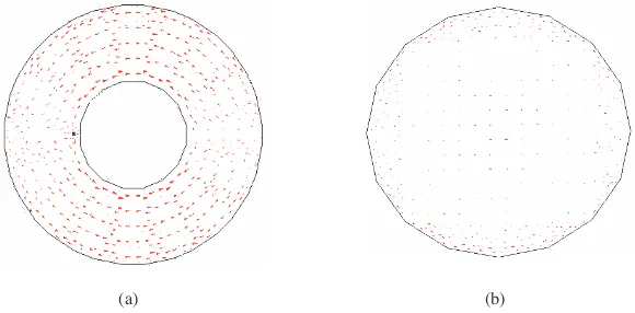
Figure 7. Current distributions at frequency 2.30 GHz (a) fed patch
(a) (b)
Figure 8. Current distributions at frequency 2.49 GHz (a) fed patch
(b) parasitic patch.
-80 -60 -40 -20 0 20 40 60 80
-18 -16 -14 -12 -10 -8 -6 -4 -2 0
Angle (degrees) E-plane, theoretical H-plane, theoretical E-plane, experimental [5] H-plane, experimental [5]
Relative radiative power (dB)
Figure 9. Radiation pattern of the proposed antenna at frequency
2.23 GHz.
experimental [5] results, the optimized return loss curves for the proposed antenna are shown in Fig. 6 as a function of frequency. It is pointed out that the theoretical results are in excellent agreement with the simulated and experimental [5] results. These justify the veracity of the proposed method. The simulated current distributions at different frequencies are presented in Figs. 7 and 8. It is observed that the effect of the parasitic patch is very significant at the two frequencies. The magnitude of currents in the parasitic patch is contributed by the electromagnetic coupling through air-gap between the two patches.
-80 -60 -40 -20 0 20 40 60 80 -25
-20 -15 -10 -5 0
Angle (degrees) H-plane, theoretical E-plane, theoretical H-plane, experimental [5] E-plane, experimental [5]
Relative radiative power (dB)
Figure 10. Radiation pattern of the proposed antenna at frequency
2.53 GHz.
proposed antenna were carried out usingEquations (15)–(20); the data so obtained are shown in Figs. 9 and 10. These figures depict that the theoretical radiation patterns at 2.230 GHz and 2.530 GHz are very close to the experimental radiation patterns at that frequencies. It is
found that the 3-dB beam widths ofE- andH-plane radiation patterns
at frequency 2.230 GHz are 81.4◦ and 80.2◦ respectively. Moreover,
66.2◦ and 74.4◦ beam widths ofE- andH-plane patterns are obtained
at 2.530 GHz, respectively.
4. CONCLUSIONS
It is, therefore, concluded that the air-gap spacing, superstrate thickness and feedingpoint location have crucial effects on the
performance of the proposed antenna. The proposed antenna has
frequency band of operation of 332 MHz (bandwidth 13.96%) that can be applied in the industrial, scientific and medical (ISM) areas.
REFERENCES
1. Dahele, J. S. and K. F. Lee, “Characteristics of annular ring
microstrip antenna,” Electronics Letters, Vol. 18, No. 24, 1051–
2. Liu, H. and X. F. Hu, “Input impedance analysis of microstrip
annular ringantenna with thick substrate,” Progress In
Electromagnetics Research, PIER 12, 177–204, 1996.
3. Lee, K. F. and J. S. Dahele, “Two layered annular ringmicrostrip
antenna,” International Journal of Electronics, Vol. 61, No. 2,
207–217, 1986.
4. Fan, Z. and K. F. Lee, “Input impedance annular ringmicrostrip
antennas with dielectric cover,” IEEE Trans. Antenna Propagat.,
Vol. 40, No. 8, 992–995, Aug. 1992.
5. Al-Charchafchi, S. H., W. K. W. Ali, and S. Sinkeree, “A stacked
annular ringmicrostrip patch antenna,” IEEE Antenna Propag.
Society Int. Symp., Vol. 2, 948–951, Jul. 1997.
6. Misra, S. and S. K. Chowdhury, “Concentric microstrip ring
antenna: Theory and experiment,” Journal of Electromagnetic
Waves and Applications, Vol. 10, No. 3, 439–450, 1996.
7. Garcia, Q. G., “Broadband attacked annular ring,”IEE Antenna
and Propogation Conference, No. 407, 508–512, Apr. 1995. 8. Ansari, J. A., R. B. Ram, S. K. Dubey, and P. Singh, “A
frequency agile stacked annular ringmicrostrip antenna usinga
Gunn diode,”Smart Materials and Structures, Vol. 16, 2040–2045,
2007.
9. Liu, Z. F., P. S. Kooi, L. W. Li, M. S. Leong, and T. S. Yeo, “A method for designing broad-band microstrip antennas in
multilayered planar structures,”IEEE Trans. Antenna Propagat.,
Vol. 47, No. 9, 1416–1420, Sept. 1999.
10. Garg, R., P. Bhartia, I. Bahl, and A. Ittipiboon, Microstrip
Antenna Design Handbook, Artech House, Norwood, MA, 2001. 11. Derneryd, A. G., “Analysis of the microstrip disc antenna
element,” IEEE Trans. Antenna Propagat., Vol. 27, No. 5, 660–
664, 1979.
12. Bahl, I. J. and P. Bhartia, Microstrip Antenna, Artech House,
Bostan, MA, USA, 1980.
13. Lee, K. F. and J. S. Dahele, “Theory and experiment on the
annular ringmicrostrip antenna,”Ann. Telecomm., Vol. 40, No. 9,