R E S E A R C H
Open Access
Configurable
M-factor VLSI DVB-S2 LDPC decoder
architecture with optimized memory tiling design
Gabriel Falcao
1,2*, Marco Gomes
1,2, Vitor Silva
1,2, Leonel Sousa
3,4and Joao Cacheira
2Abstract
Semi-parallel architectures for decoding Digital Video Broadcasting-Satellite 2 (DVB-S2) Low-Density Parity-Check (LDPC) codes have improved Very Large Scale Integration (VLSI) solutions, but their design is challenging from several perspectives. In order to conveniently exploit parallelism for obtaining VLSI LDPC decoders that occupy small circuit areas and demand low power consumption, we propose in this article a novel ASIC reconfigurable approach that exploits efficiently the memory block reshaping required to use a reduced number of processor nodes. We exploit different memory tiling configurations to reduce the memory area about 20%. The proposed architecture was synthesized for a 90 nm process design with a variable number of processor nodes and a
competitive circuit area of 6.2 mm2was achieved. The operating frequency simultaneously guarantees throughputs superior to 90 Mbps, as required by DVB-S2, and low levels of power consumption.
Keywords:LDPC decoding, DVB-S2, VLSI, ASIC, memory tiling, semi-parallel architecture,M-factorizable architecture, Low-power consumption, high-throughput
1 Introduction
Over the last 15 years Low-Density Parity-Check (LDPC) codes have assumed a growing importance in the channel coding arena, namely because they have error correction capability to achieve efficient coding close to the Shannon limit. These codes were invented by Robert Gallager (MIT) in the early sixties [1] and have never been fully exploited due to overwhelming computational requirements by that time. LDPCs are linear block codes (N,K) and can be described by sparse binary parity-checkHmatrices with dimensions (N - K) × N. They can also be elegantly represented by a Tanner graph [2] defined by edges connecting two distinct types of nodes usually denoted as Bit Nodes (BN), with a BN for each one of theNvariables of H, and Check Nodes (CN), also called restriction or test nodes, with a CN for each one of the (N - K) parity-check equations given by H. Naturally, the fact that their patent has expired, has shifted the attention of the scientific community and industry away from Turbo codes [3] towards the study of LDPC codes [4], which quickly have shown to be able
of guaranteeing similar or even superior coding perfor-mance. Mainly for these reasons and also because advances in microelectronics allowed the development of hardware solutions for real-time decoding, LDPC codes have been adopted by modern communication standards [5-7]. Important examples of these standards are: the Digital Video Broadcasting-Satellite 2 (DVB-S2) for satellite communications [8]; the WiMAX IEEE 802.16e for wireless communication systems in Metro-politan area networks (MAN) [9]; the WiFi 802.11n standard for wired home networking technologies; and the 10 Gb Ethernet IEEE 802.3an. Also, the introduction of LDPC codes in 4G systems has recently been pro-posed, as opposed to Turbo codes adopted in 3G. Some of these applications impose challenges that typically have to be addressed by using dedicated solutions that require System-On-Chip (SoC) hardware providing at the same time good performance, low power consump-tion and small die areas. Naturally, special emphasis has been given to solutions addressing the DVB-S2 standard for satellite communications [8], which represents the most challenging application that actually incorporates the use of LDPC codes.
In the past we have seen that parallelism can be effi-ciently exploited to achieve good performances with * Correspondence: [email protected]
1
Instituto de Telecomunicações, Pólo II - Universidade de Coimbra, 3030-290 Coimbra, Portugal
Full list of author information is available at the end of the article
iterative message-passing algorithms used in LDPC decoding [10-12]. However, LDPC codes with good cod-ing performances demand very long lengths [4,13], as it is the case of those adopted in the DVB-S2 standard. The development of efficient Very Large Scale Integra-tion (VLSI)-hardware able of providing the huge compu-tational power necessary and performing irregular memory accesses in real-time actually represents a real challenge. Focused on the original architecture devel-oped by Kienle et al. [5] that usesM = 360 processor nodes, we investigated and developed efficient hard-ware-dedicated DVB-S2 LDPC decoders, namely by using a reduced number submultiple of M of light-weight node processors. Consequently, we have also reduced significantly the routing complexity of the inter-connection network between processor nodes and mem-ory blocks, which represents a target that aims to improve the design in terms of cost and complexity. This architecture has been initially proposed in [14], but some important challenges have not been addressed yet. In this article we tackle these challenges, namely by materializing the benefits and quantifying the gains achieved with the VLSI design of this architecture, in particular regarding the complex design of Application Specific Integrated Circuit (ASIC) memory blocks that can benefit from the use of the reduced number of pro-cessors. The proposed architecture exploits themodulo
-mproperties of DVB-S2 codes that allow to take advan-tage of partial parallelism to increase throughput perfor-mance. Because we propose a reduction of the number of processors used, we also address the necessary mem-ory blocks reshape. Although the amount of stored bits remains the same independently of the number of pro-cessors, we show that the memory configuration for a solution that uses less processing units is more efficient in terms of circuit area. The architecture has been pro-totyped using ASIC technology. Synthesis results show that the proposed solution achieves high performance with low power consumption and within a small circuit area context. We also present synthesis results for a memory optimized ASIC architecture that compare well with those reported in state-of-the-art solutions of DVB-S2 LDPC decoders [5-7,15,16]. The main contribu-tions of the article are: (i) efficient, scalable and parallel architectures with any submultiple of M = 360 number of processors for VLSI-based LDPC decoders under the context of DVB-S2; (ii) optimized synthesis area results for different sets of functional units and corresponding memory blocks reconfiguration; (iii) architecture with reduced routing complexity, occupying small die areas and consuming low power; and (iv) decoders with high throughput.
This article is organized as follows. In the next section we describe structured DVB-S2 LDPC codes. In Section
3 we present an overview of the state-of-the-art and also the main challenges regarding the development of effi-cient VLSI LDPC decoders for DVB-S2. Section 4 addresses theM-factorizable parallel approach proposed, and in Section 5 we describe an optimized RAM mem-ory design procedure for ASIC. Section 6 presents experimental results for the proposed LDPC decoder architecture synthesized for ASIC and compares its per-formance with other architectures in the literature. Sec-tion 7 concludes the article.
2 LDPC codes
Graphical models, and in particular Tanner graphs [13], have often been proposed to perform approximate infer-ence calculations [17,18]. They are based on iterative intensive message-passing algorithms [19] also known as Belief Propagation (BP) that perform the computation of joint probabilities on graphs (as depicted in Figure 1) and are commonly used in information theory (e.g., channel coding), artificial intelligence and computer vision (e.g., stereo vision) [17], which, under certain cir-cumstances, can become computationally prohibitive.
2.1 LDPC decoding
In this article we are interested in the BP algorithm applied to LDPC decoding. In particular, we exploit the Min-Sum Algorithm (MSA), an efficient simplification [13] of the Sum-Product Algorithm (SPA), which is very demanding from a computational perspective. The MSA here applied to LDPC decoding operates over Log-likeli-hood Ratios (LLR) [1], exchanging information and updating messages between neighbor nodes over succes-sive iterations. From a computational perspective, this simplification decreases the complexity of processing because it uses sum operations instead of multiplica-tions, while subtractions replace divisions [13,20]. Although this represents a lower workload than the one required by the SPA, it is still quite significant. If the number of nodes is large–in the order of thousands as in the case of DVB-S2–the MSA can still demand very intensive processing [13,19].
for short length codes, in [22] it is successfully extended to DVB-S2 LDPC codes. This fact, associated with the corresponding and relatively simple changes necessarily introduced in the design of the architecture, is the main reason why we adopted the l -min = 1 solution [24], which computes LLR messages based on two minimums.
The SPA can also be performed in the logarithmic domain as described in [20]. In the next equations,Lpn
designates thea priori LLR of BNn, derived from the
values received from the channel, andLrmn is the
mes-sage that is sent fromCNmto BNn, computed based on
all received messages from BNs of group N(m)\n, where N(m)\n represents BNs connected to CNm
excluding BNn, according to:
Lrmn= represents an overestimation of LLR calculated values, which can be compensated by using the improved nor-malized MSA algorithm [22,23] with two normalization factors (this was the solution adopted in our architec-ture). Consequently, (1) becomes:
Lrmn=α×
whereacan be obtained by:
α=
α1 ⇐ if Lrmn== first minimum
α2 ⇐ if Lrmn== second minimum. (5)
Also,Lqnm is the LLR of BNn, which is sent to CNm
and calculated based on messageLpnreceived from the
channel and from CNs of M(n)\m, where M(n)\m represents the set of CNs connected to BNn excluding
Check Node 0 updating
Bit Nodes 0, 1 and 2 Check Node 1 updatingBit Nodes 3, 4 and 5 Check Node 2 updatingBit Nodes 0, 3 and 6
CN0
CNm, and is given by:
Lqnm=Lpn+
m∈M(n)\m
Lrmn. (6)
At the end of each iteration we compute thea poster-ioriLLRs of BNs,
LQn=Lpn+
m∈M(n)
Lrmn (7)
and perform hard decoding to obtain the decoded output wordĉ[13,19]
ˆ
Before the first iteration occurs, for each node pair (BNn, CNm), we initializeLqnm with the LLR
informa-tion Lpn received from the channel, and then we
pro-ceed to the iterative body of the algorithm until stop conditions occur: HĉT ≠0 or the maximum number of iterations is reached.
2.2. DVB-S2 LDPC codes
Following the recognition of their potential, LDPC codes have been recently adopted by DVB-S2 [8] and other new standards for communication and storage applica-tions. They use their powerful coding gains, obtained at the expense of computational power, to achieve good performances under adverse channel conditions. Some of the LDPC codes adopted in those standards have a periodic nature, which allows exploiting suitable repre-sentations of data structures for reducing the computa-tional requirements. These modulo-m properties of DVB-S2 LDPC codes are described next, in order to allow understanding how architectures can take advan-tage of them, namely for exploiting parallelism.
The Forward Error-correcting (FEC) system of the recent DVB-S2 standard [8] incorporates a special class of LDPC codes based on Irregular Repeat Accumulate (IRA) codes [25]. The parity-check matrix His of the form:
whereAis sparse and hasmodulo-m properties, and Bis a staircase lower triangular matrix. The structured constraints put on the pseudo-random generation of matrix Aallow a significant reduction on the storage requirements without significant code performance loss. The N bits of a codeword are represented in the sys-tematic form, divided in information bits (IN) and par-ity-check bits (PN) given by the number of columns of AandB, respectively. The construction technique used to generate the Amatrix consists of splitting the IN nodes into disjoint groups ofM =360 consecutive 1’s. All the IN nodes of a group l should have the same weight wl and it is only necessary to choose the CN
nodes that connect to the first IN of the group, in order to specify the CN nodes that connect to each one of the remaining (M -1) IN nodes of that group. The connec-tion choice for the first elements of groupl is pseudo-random but it guarantees that, in the resulting LDPC code, all the CN nodes must connect to the same num-ber of IN nodes. Denoting byr1,r2,. . .,rwlthe indices of
the CN nodes that connect to the first IN of group l, the indices of the CN nodes that connect to INi, with 0
≤i≤M -1, of grouplcan be obtained by:
(r1+i×q)mod(N−K), (r2+i×q)mod(N−K),. . ., (rwl+i×q)mod(N−K), (10)
with
q= (N−K)/M. (11)
The parameterM = 360 is constant for all codes used in the DVB-S2 standard. For each code, the first groups of IN that formAhave constant weightswb>3, and the
remaining groups have weights wb=3. MatrixBhas a
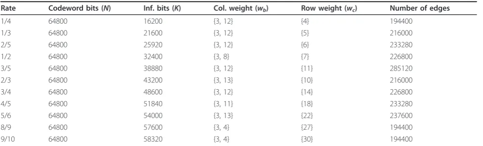
lower triangle staircase profile as shown in (9). The LDPC codes adopted by the DVB-S2 standard support two different frame lengths, one for short frames (N= 16, 200 bit) and the other for normal frames (N =64, 800 bit). The short frame mode supports ten distinct code rates as depicted in Table 1, while the latter sup-ports 11 rates as shown in Table 2. The column and row weights are also depicted in Tables 1 and 2 for all rates in the standard. For short frame lengths, only 50% of the codes have constant weight wc as indicated in
Table 1, while for normal frame length codes all CNs have a constant weightwc, as indicated in Table 2.
Both tables show the number of edges for each code adopted in the DVB-S2 standard. In each edge circulate messages (Lrmn andLqnm) that are used to update the
>219 messages are exchanged per iteration, which imposes significant computational demands (at several levels) for the development of LDPC decoders.
3 Overview of VLSI LDPC decoding architectures The two types of nodes (BN and CN) in the Tanner graph require distinct processing. Therefore, processor nodes of LDPC decoding architectures must be capable of performing these two types of calculations in order to compute the improved normalized MSA. Also, it is necessary to incorporate memory to store messages associated with each processor node, and the decoder requires an efficient switching mechanism to allow each processor node in the graph to access different memory banks. Ideally, this should be performed in parallel to increase throughput. The message-passing scheduling mechanism controls the order in which messages are updated (i.e., the order how memory is addressed by each node processor), defining which nodes communi-cate with each other and in what order. A control logic unit, dependent on scheduling, controls the interconnec-tion network that performs this task. It connects
existing BN (usually a factor of N) with CN (usually a factor of (N - K)) processors to the corresponding mem-ory blocks, in order to allow read/write operations (to be performed in parallel) into different blocks that store subsections of the graph. The interconnection network should be designed to allow conflict-free accesses to memory banks.
3.1 Parallel LDPC decoder architectures
The complex nature of such a VLSI architecture pre-sents several challenges. To perform fast LDPC decod-ing, it requires a certain level of parallelism, which should have some significance in order to achieve a throughput that can be very demanding (90 Mbps in the DVB-S2 case [8]). Above some level of parallelism the requirements for routing, area and power consumption may be difficult to achieve for practical reasons. Pre-sently, there are LDPC decoder architectures ranging from serial [26] to fully parallel [10], targeting different objectives. Serial decoders trade throughput with archi-tectural simplicity, obtaining reduced die areas. Although limitations at the processing level can make
Table 1 Properties of short frame length DVB-S2 codes
Rate Codeword bits (N) Inf. bits (K) Col. weight (wb) Row weight (wc) Number of edges
1/4 16200 4050 {3, 12} {4}* 48600
1/3 16200 5400 {3, 12} {5} 54000
2/5 16200 6480 {3, 12} {6} 58320
1/2 16200 8100 {3, 8} {6}* 48600
3/5 16200 9720 {3, 12} {11} 71280
2/3 16200 10800 {3, 13} {10} 54000
3/4 16200 12150 {3, 12} {12}* 48600
4/5 16200 12960 {3} {14}* 45360
5/6 16200 13500 {3, 13} {19}* 51300
8/9 16200 14400 {3, 4} {27} 48600
Properties of LDPC codes (the five short frame codes marked with the symbol * don’t have a constant weight per rowwc, since they have been shortened has defined in the standard [8]. Consequently, they have rates which are an approximation to those mentioned in this table, but not exactly the same.) used in the DVB-S2 standard [8] for the short frame length
Table 2 Properties of normal frame length DVB-S2 codes
Rate Codeword bits (N) Inf. bits (K) Col. weight (wb) Row weight (wc) Number of edges
1/4 64800 16200 {3, 12} {4} 194400
1/3 64800 21600 {3, 12} {5} 216000
2/5 64800 25920 {3, 12} {6} 233280
1/2 64800 32400 {3, 8} {7} 226800
3/5 64800 38880 {3, 12} {11} 285120
2/3 64800 43200 {3, 13} {10} 216000
3/4 64800 48600 {3, 12} {14} 226800
4/5 64800 51840 {3, 11} {18} 233280
5/6 64800 54000 {3, 13} {22} 237600
8/9 64800 57600 {3, 4} {27} 194400
9/10 64800 58320 {3, 4} {30} 194400
them target mainly low-throughput applications, they can exploit hardware simplifications, such as reducing the storage size of messages and still achieve coding gains without noticeable loss in performance [26]. Paral-lel approaches offer superior throughput at the expense of architectural complexity and circuit area. On a fully parallel system, the complexity increases significantly as the code length grows. The dimension and complexity of this type of architectures are only acceptable for short to medium length LDPC codes. One of the first LDPC decoder on ASIC [10] is based on a fully parallel architecture for a 1, 024 bit, rate = 1/2 LDPC decoder processing 64 iterations, that obtains a throughput of 1 Gbps. The excellent performance achieved is only possi-ble due to the complex routing established to connect all N BN processors with corresponding (N - K) CN processors. Consequently, the complex wiring of the cir-cuit created the need to carefully manage the floor plan-ning and routing of the design, which alerted for the prohibitive complexity involved in the design of archi-tectures that support block codes with high lengths (N >1,024 bit).
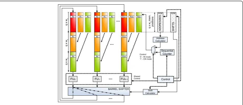
Naturally, the size of the architecture is influenced by the length of the largest code supported and also by the level of parallelism adopted. This has direct implications in the number of node processors necessary to perform computation and, more importantly, in the complexity of the interconnection network (represented by a barrel shifter in Figure 2). The complexity of this network decreases by reducing the level of parallelism of the architecture. For a fixed code, permutation patterns are known a priori and the indices/addresses that indicate which nodes connect with each other are usually com-puted offline. Compared with full-parallel decoders, the
complexity of an interconnection network in a partial-parallel architecture significantly decreases, which elimi-nates important restrictions from the routing process (in the place & route phase of the design).
Partial-parallel architectures for high-throughput LDPC decoding have been proposed by Mansour et al. [11,12], where the concept of architecture-aware LDPC codes was firstly introduced. Architecture-aware codes decouple the architectural dependence of the decoder from the LDPC code properties. They achieve a faster convergence rate, which allows obtaining higher throughputs [12]. In this case, the interconnection net-work can be efficiently implemented by using program-mable multi-stage networks [11]. A comparison between serial, partly-parallel and full-parallel architectures has been performed by Fanucci et al. in [27] for a regular code withN= 2,048 bits, wc= 6 and wb= 3. However,
these architectures are dedicated to particular cases and other solutions were necessary to support other types of more demanding LDPC codes, namely those that have irregular nature and higher block lengths.
For long length LDPC codes (e.g., DVB-S2 codes), typically more than 70% of the circuit’s area in VLSI decoders is occupied by memory units [6,15], which are essential to support the iterative message-passing mechanism. They are extensively addressed in the con-text of this article. Memory requirements for parallel architectures capable of supporting long length codes are feasible, but hard to achieve for practical reasons on a VLSI approach. The number of accesses and the amount of memory necessary to store messages exchanged between hundreds or thousands of nodes is extremely high, which imposes restrictions in die area and power consumption. Although in a partial-parallel
SH
approach the total amount of memory necessary to store messages remains unchanged for any number of proces-sors, by varying the latter, the height and width of mem-ory blocks change, which can be exploited to achieve architectures with more efficient areas.
3.2 ParallelM-kernel LDPC decoder architectures for DVB-S2
The development of LDPC decoders for the DVB-S2 standard can be considered to be among the most demanding applications for this type of processing, mainly due to the high length of codes adopted [8]. LDPC codes used in this standard are IRA codes, where the sparse parity-checkHmatrix hasmodulo-m proper-ties that can be exploited to achieve hardware paralle-lism [25].
The use of scalable parallelism to obtain chips with small areas for DVB-S2 has been proposed for technolo-gies ranging from 0.13µm down to 65 nm [5-7,15,16] based on the processing of sub-sets of the Tanner graph, which guarantee the minimum necessary throughput of 90 Mbps required by the standard [8]. The design of partial-parallel solutions generates sys-tems with lower areas, but also implies lower through-puts, comparing to full-parallel architectures in a SoC. One of the architectures initially proposed by Kienle et al. [5] uses M =360 processor nodes, also referred in this text as Functional Units (FU). They work in parallel and share control signals, that process both CN nodes (in CN mode) and IN nodes (in BN mode) according to a flooding schedule approach.
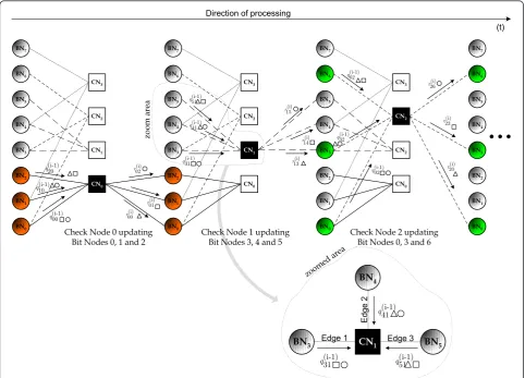
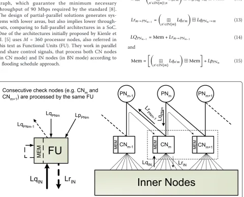
Attending to the zigzag connectivity [8] between PNs and CNs defined byBin (9), they are updated jointly in CN mode [5]. An efficient VLSI architecture has been proposed in [28,29], where the joint processing of CNs and PNs is performed as depicted in Figure 3. For example, when updating PNm, according to (6) it
becomes a passing node because the message it sends to CNm+1 is the message received from CNm added to the channel information, and vice-versa (see Figure 3). Since each FU processes q consecutive CNs, the update of PNs follows an horizontal schedule approach, with PNs and CNs being processed simultaneously. This schedul-ing mechanism allows a faster decodschedul-ing convergence [30]. Therefore, the message that travels through CNm,
PNm and CNm+1 is kept in the FU and only the back-ward message that is sent from CNmto PNm-1is saved in the external memory. The equations that describe the operation inside the FU in CN mode are [29]:
Lrmn=
n∈IN(m)\nLqn
m
LqPNm→mMem (12)
Lrm→PNm−1 =
n∈IN(m)Lqn
m
LqPNm→m (13)
LQPNm−1 = Mem +Lrm→PNm−1 (14)
and
Mem =
n∈IN(m)Lqn
m
Mem
+LpPNm (15)
CNm
CNm-1 CNm+1
PNm
PNm-1 PNm+1
MEM
MEM MEM
LqIN LrIN
LqPN
m
Lr
PNm -1
MEM
Consecutive check nodes (e.g. CNm and
CNm+1) are processed by the same FU
Lq
INLr
INLqPNm
LqPNm-1
LpPNm
where IN(m) represents the set of INs connected to CNm, and Mem is the internal memory of the FU.
All 360 FUs process one message per cycle. In IN mode, the 360 messages are read from the same address (sequentially incremented, for this type of processing) in the respective memory blocks. The new messages result-ing from this computation are then stored in the same address cyclically shifted right through the interconnec-tion network, implemented by a barrel shifter. The
mod-ulo-mproperties of LDPC codes used in DVB-S2 allow
to replace the complex interconnection network by a common barrel shifter. In CN mode, messages have to be read from specific addresses and stored back in the same addresses cyclically shifted left to conclude the execution of an iteration. Once again, the access is per-formed in parallel for all 360 messages. The barrel shif-ter mechanism and the efficient memory mapping scheme constitute the major strengths of the architec-ture described in [5].
Memory requirements for a partially parallel architec-ture capable of supporting long length codes used in DVB-S2 are demanding. The appropriate Controlof
ADDRESSES and SHIFTS memory banks indicated in
Figure 2 guarantees that every time the address of a memory block changes, it changes accordingly and with-out conflicts for allM = 360 processors in parallel. The barrel shifter, which has a switching activity controlled by theSHIFTSmemory bank, can be properly managed together with the ADDRESSES memory block that defines memory accesses, to simulate the connectivity of the Tanner graph. In [5] it is illustrated the memory mapping mechanisms used in BN processing as a func-tion ofq(a parameter defined by the standard), which is presented in (11). In CN processing, a similar scheme applies. For each different code we use different SHIFTS
and ADDRESSES values, which can be easily obtained
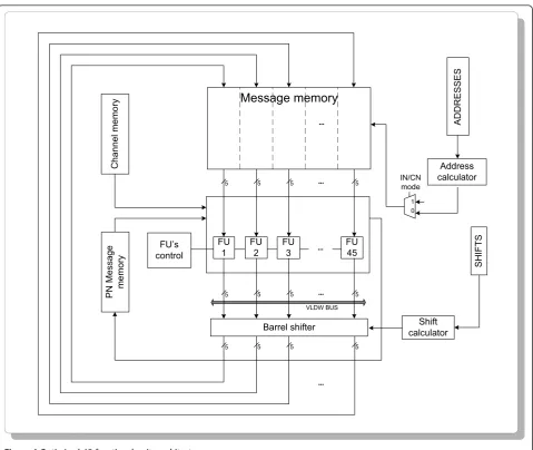
from annexes B and C of the DVB-S2 standard [8]. In Figure 4 mainly three distinct types of memory are depicted: (i)Channel memory which initially receives data (IN and PN) from the input of the LDPC decoder;
(ii)Messagememory, where all messages associated with
information bits are stored (the FU supports both types of BN and CN processing, which perform alternately during the same iteration); and (iii) PN Message mem-ory that holds messages associated with parity bits, which are computed in CN mode and have all weight
wc = 2 (zigzag connectivity depicted in Figure 3). InPN
Messagememory each FU only needs to store the
mes-sage which is passed during the backward update of CNs [14].
However, the large number of FUs used (360) still implies a wide and complex barrel shifter that requires a significant die area and imposes routing problems in order to accommodate the simultaneous accesses of all
360 FUs to corresponding messages in memory. Since this architecture is able to provide, with the current technology, a throughput far above the mandatory 90 Mbps, we are able to reduce the number of FUs even further. In fact, we herein show that this can be done by any integer factor submultiple of M = 360, which, for VLSI systems, presents a beneficial reduction of the size of the barrel shifter.
4 M-factorizable VLSI parallel LDPC decoder architecture for DVB-S2
Under this context we developed a novel hardware approach, originally proposed in [14,28], which is based on a partial-parallel architecture that simplifies the bar-rel shifter and reduces memory requirements. We address the generalization of the well known M-kernel parallel hardware structure [5] and propose its partition-ing by any integer L submultiple of M (which can be obtained from the decomposition of M= 360 = 23 × 32 × 5), without memory addressing/reconfiguration over-heads and keeping unchanged the efficient message-pas-sing mechanism. The proposed architecture provides an efficient way of reducing the number of FUs and the overall complexity of the decoder. This approach does not only surpass some disadvantages of the architecture described in [5], such as die area occupied or routing congestion, but it also adds flexibility and reconfigurabil-ity to the system according to the decoder requirements and device constraints. This type of sub-sampling approach preserves the key modulo-mproperties of the architecture [5], with only P =M/L processing units addressed in [28,29] as shown in Figure 2. This strategy allows a linear reduction byLof the hardware resources occupied by the FU blocks, and reduces significantly the complexity (2 ×O(PlogP)) of the interconnection net-work (or barrel shifter), which simplifies the routing problem. This strategy does not imply an increase by L
in the size of ROM memories (that hold SHIFTS and
ADDRESSESvalues). In fact, by performing a
sub-sam-pling byL, each group of M =360 INs or CNs results in L subgroups of PINs or CNs. As the properties of the first subgroups of CNs and BNs to process are known, the modulo-m periodicity of DVB-S2 codes allows to automatically calculate the properties of the remaining subgroups. Based on the SHIFTS shift0 to apply to the first subgroup, we can obtain the remaining subgroupsg, with 0≤g≤L -1 by [14]:
shiftγ = (shift0+γ)divL. (16)
The same applies forADDRESSES, which can be com-puted as:
For the architecture to support onlyPFUs (instead of theM = 360 FUs as in [5]), memory blocks have to be reorganized according to (16), (17) and Figures 2 and 5. We can reshape these memory blocks and keep unchanged the size of the system ROM, by computing on the fly the new SHIFTSas a function of those initi-ally stored in the ROM, as indicated in (16). In the con-figuration shown in Figure 2, each FUi, with 0< i < P
-1, is now responsible for processing information (IN), parity (PN) and CN according to a proper memory mapping and shuffling mechanism. As we increase L, the smaller become the sub-sets of the Tanner graph processed in parallel. Figure 5 describes the addressing mechanisms used in the factorizable architecture forL =
2, which uses 180 FUs. The amount of memory is exactly the same as in the architecture withL = 1, but the structure is different. There are less FUs and the
corresponding memory word size decreases. As shown in Figure 2, memories have to become higher and thin-ner in order to hold the same information as before. This new memory configuration will introduce benefits in area occupied by the architecture, as it will be shown later.
5 Optimizing RAM memory design based on macro cells for ASIC
The presented architecture has been described in Regis-ter Transfer Level (RTL) forP ={45, 90, 180, 360} FUs. All solutions use 5-bit to represent data messages. Fig-ure 2 shows that all four configurations use exactly the same amount of memory, though rearranged with differ-ent widths and heights (distinct memory dimensions). The smaller the number ofP functional units adopted, the higher and thicker block memories become. The
Ch
an
ne
l me
mo
ry
PN Messa
ge
me
mo
ry
FU’s control
Barrel shifter calculatorShift
SHIFTS
Address calculator
IN/CN mode
AD
D
R
ESS
ES
FU 45 FU
3 FU
2 FU
1
0 1
Message memory
5
5 5
5 5
5
5
5
5 5 5 5
VLDW BUS
complete type and amount of memories necessary for such design are:
•Messagememory holds internal messages calculated
during each iteration of the decoding process asso-ciated with IN;Messagememory width (word length) is given bywa=number of FU × message, which in
this caseis wa= M ×5/Lbits; the heighthmmcan be
obtained for worst case scenario (code with rate = 3/5 obtained from Table 2, where the number of edges is maximum). In this case,hmm= L × q × (wc-2);
•Channel memory stores IN and PN data incoming
from the channel. This memory has the same word length as Message memory (wch = wa), and the
height is given by hch=L× 64800/M, representing
the worst case (normal frame);
•PN message memory holds messages calculated
during each iteration, which are associated only with parity bits. It has the same width asChannel mem-ory and the heighthPN=L × qis obtained for worst
case scenario (code withrate = 1/4) from Table 2, which turnsq = 135 (only one 5-bit message per each parity bit has to be stored);
• Hard decoding memory holds IN and PN data
obtained in the hard decoding phase of processing (1-bit per FU); the width of this memory is given by the number M/LFUs of the architecture, and the heighthHDis obtained fromhHD=L× 64800/M.
Table 3 summarizes the required width and height (mem. pos.) of all memories used in the four synthesized configurations. Unfortunately, sometimes RAM memory
358q
359q-1 359q
360q-1
4q-1
3q 3q-1
2q 0
2q-1
q-1 q
FU0 FU1 FU179
Barrel
Shifter
Message mapping CNs
Message mapping INs
0 360
1 361
360q-359 2 362
3 363
360q-357
358 718
360q-2
719
358q+1
358q+2
2q+1 2q+2 1
2
1rst group
2nd group
Legend: 359
360q-1
359q+1
359q+2
3q+2
3q+1 q+2
q+1
360q-358 360(q-1)
B
N
wei
ght
wb
CN wei
ght
wc
Figure 5Memory organization usingM= 180 functional units. Memory organization for the computation ofLrmnandLqnmmessages,
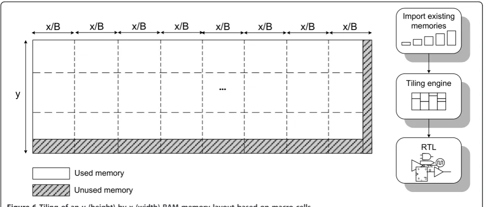
libraries of macro cells do not exactly support all the specified heights requested in Table 3, but rather stan-dard dimensions which are usually a power of 2, as shown in Table 4. The area results obtained in the synthesis process and shown in Table 5 allowed other interesting conclusions. Memories occupy nearly 97% of the circuits’total area. The remaining part of the circuit is occupied by the barrel shifter, the functional units and the control logic. The fact that in the four config-urations the areas are different was also a surprise. Table 5 shows these differences. As mentioned before and depicted in Figure 2, the total amount of memory is the same for all designs. If we realize that they occupy a significant area of the design, we conclude that their dif-ferences should be minimal. To analyze these differ-ences, we first need to understand how memories are generated and the RAM generator limitations. The architecture implemented in RTL uses memories with large width (word length) and height (number of words, or memory positions).
The RAM generator used can create memories that support the requested number of words, but the maxi-mum word width is limited to 64 bits, which is far below the architectural needs. To overcome this pro-blem, B blocks of RAM memory were concatenated until the required width was achieved, as shown in Fig-ure 6. Each RAM memory has its own internal control logic which can address data in the operating clock cycle, with its own antenna diode protection, testing mechanisms, power rings, etc. As represented in Figure 6, more memories are necessary for large words, which replicates control hardware and increases silicon area. This seemed to show that some level of inefficiency should be expected. A practical example with real areas can be addressed for theMessageRAMs for 360 and 45
FUs, to give a better perspective of the problem. In the former configuration, theMessage RAM width is 1,800 bits (5 bits per message × 360 FUs) with 210 addresses (height). For the second configuration, the RAM width is 225 bits (5 bits per message × 45 FUs) with 213 addresses. Both Messagememory blocks have the same capacity (210 × 1, 800 bits), however the area used by the wider 360 FUs Messagememory is 6.2 mm2, while the thiner 45 FUs memory occupies only 3.2 mm2. These memories were created by concatenatingBbanks of 45 bit RAMs, as illustrated in Figure 6. For 360 FUs, 40 instantiations are necessary (40 × 45 bits = 1,800 bits) while for 45 FUs only five instantiations are needed (5 × 45 bits = 225 bits). Whatever the factorization level
L adopted, the architecture will still have to support a Very Long Data Word (VLDW) bus. This property is illustrated in detail in Figure 4, where the VLDW bus implies a complex routing of the wiring associated with it. This introduces additional complexity managing the floor planning and routing process (in the place & route phase of the design). Nevertheless, the architecture with 45 FUs minimizes this problem by moving its complex-ity to a dimension where it can be more easily tractable.
5.1 Minimal RAM memory configuration
From all designs in Table 5 the architecture with 45 FUs occupies the smallest area. Comparing Tables 3 and 4, we notice that due to hardware restrictions, there is a
Table 3 Required RAM memory size for each configuration
Type of RAM 360 FUs 180 FUs 90 FUs 45 FUs
(mem. pos. × width)
Message 648 × 1800 1296 × 900 2592 × 450 5184 × 225
Channel (IN + PN) 180 × 1800 360 × 900 710 × 450 1440 × 225
PN message 135 × 1800 270 × 900 540 × 450 1080 × 225
Hard decoding (IN + PN) 180 × 360 360 × 180 720 × 90 1440 × 45
Table 4 Physical (real) RAM memory size for each configuration
Type of RAM 360 FUs 180 FUs 90 FUs 45 FUs
(mem. pos. × width)
Message 210× 1800 211× 900 212× 450 213× 225 Channel (IN + PN) 28× 1800 29× 900 210× 450 211× 225 PN message 28× 1800 29× 900 210× 450 211× 225 Hard decoding (IN + PN) 28× 360 29× 180 210× 90 211× 45
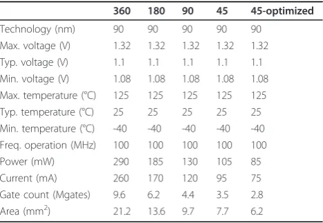
Table 5 Optimized synthesis results for ASIC
360 180 90 45 45-optimized
Technology (nm) 90 90 90 90 90 Max. voltage (V) 1.32 1.32 1.32 1.32 1.32 Typ. voltage (V) 1.1 1.1 1.1 1.1 1.1 Min. voltage (V) 1.08 1.08 1.08 1.08 1.08 Max. temperature (°C) 125 125 125 125 125 Typ. temperature (°C) 25 25 25 25 25 Min. temperature (°C) -40 -40 -40 -40 -40 Freq. operation (MHz) 100 100 100 100 100 Power (mW) 290 185 130 105 85 Current (mA) 260 170 120 95 75 Gate count (Mgates) 9.6 6.2 4.4 3.5 2.8 Area (mm2) 21.2 13.6 9.7 7.7 6.2
portion of the RAM which is never used. The 45 FUs architectureMessage RAM, for instance, needs 225 × 5184 = 1,166,400 bits. But physically, we have 225 × 213 = 1,843,200 bits, resulting in about 37% unused bits. This fact occurs in all memories and for all architectures and we tried to minimize it by using decompositions into powers of 2 and concatenating smaller RAMs, but we realized that instead of decreasing, the area increases nearly 30%, which can be justified by the additional number of internal RAM hardware controllers incorpo-rated into the design. However, joining together several blocks of memory that operate in different time slots into one bigger common block of memory can become a more efficient solution. By analyzing in detail the Mes-sage memory block of the architecture with 45 FUs depicted in Figure 4, each 5 bits of the word are directly connected to each FU, and consequently only one main memory block is used, as mentioned in the beginning of Section 5. Therefore, the control is unique and only one (write or read) address is needed to transfer data to/ from all FUs. This memory must be a dual port RAM, in order to allow reading and writing during the same clock cycle. However, due to memory generator limita-tions in the tools used, this type of memory was not possible to achieve. To overcome this, we adopted a solution that consists of creating a memory that oper-ates at twice the circuit’s frequency (fop): in the first cycle it performs read operations; and in the second one it writes data to memory. The system’s master clock operates at 200 MHz and it is used to feed memory blocks, while fop = 100 MHz is synchronously derived from this clock source.
The LDPC decoder input data comes from an external de-interleaver module that does not work at the same
clock frequency as the LDPC decoder. To guarantee that no information is lost, all messages delivered to the decoder must be stored in Channelmemory. The PN
messagememory is equally stored on a dual port RAM
which, due to memory generator limitations as before, was converted into a single RAM working at twice of the initial frequency. In the beginning, this memory is loaded with zeros, and then it will hold data associated with parity bits necessary in each iteration of the decod-ing process. Shift and address data are loaded from an outside source intoSHIFTS andADDRESSESmemories. The values stored in these memories depend on the code rate and must be previously calculated.
6 Experimental results
In the next subsections we present the obtained experi-mental results for the architecture in Figure 2, which was synthesized for ASIC using a 90 nm CMOS process design. Place & route was performed using eight metal layers. Memories were synthesized using a generic RAM generator tool with libraries of macro cells. Estimates for power consumption were obtained assuming a tog-gling rate of 10%. The architecture was also synthesized for Field-Programmable Gate Array (FPGA), but only for validation purposes [14].
6.1 Experimental synthesis results for ASIC
Synthesizing in ASIC technology the architecture withP
= {45, 90, 180, 360} FUs aims at finding the one which produces better power consumption and area results, while simultaneously supporting the throughput require-ments of the standard. The architecture supports short and normal frame lengths for all code rates, even though it is dimensioned for the worst case. All rates in
U/D Reset B1
B4
Carry out ENB Counter S1 S2 D CENB Multiplexer
x/B x/B x/B x/B
y
Used memory
Unused memory
Import existing memories
Tiling engine
RTL
Q Q
SE T CL R
S R
EN B
x/B x/B x/B
x/B
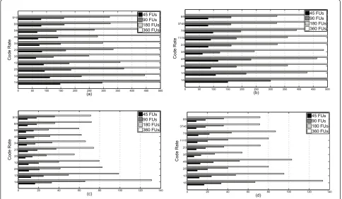
the solutions here proposed support 90 Mbps as required by the DVB-S2 standard. Figures 7a) and 7b) report throughput performance achieved for normal and short frame length DVB-S2 codes decoding ten itera-tions. For example, withP= 90 FUs (or equivalentlyL= 4) in the normal frame mode, for code with rate = 1/4 the throughput surpasses 295 Mbps, while withP = 90 FUs it reaches 1.18 Gbps. Figures 7c) and 7d) report the maximum number of iterations supported by the archi-tecture working at 100 MHz, while producing the DVB-S2 target throughput of 90 Mbps. For example, for P= 180 FUs (L= 2) in the normal frame mode, a maximum of 65 iterations is supported when decoding rate = 1/4, while 27 iterations are achieved for code with rate 3/5 (worst case working conditions for DVB-S2). Half these values are obtained withP= 90 FUs (L= 4) and a value four times inferior is achieved withP= 45 FUs (L = 8). It can also be seen that a maximum of 55 iterations is supported for the configuration withP= 90 FUs decod-ing the worst case code. Technical limitations imposed by the available library of memory macro cells, namely the maximum frequency of operation at 200 MHz and the fact that they do not support dual-port memories, have put limits on throughput and maximum number of
iterations supported. To exemplify this, our architecture implemented with P = 45 FUs supports at maximum seven iterations when decoding at a throughput of 90 Mbps for worst case working conditions, as depicted in Table 6. By using dual-port memories, or memories cap-able of supporting frequencies in the range of 400 MHz (that would allow to have the main circuit operating at 200 MHz), it would be possible to achieve 14 iterations for worst case condition (see Table 6) without additional modifications in the design, at the expense of an increase in power consumption. To validate this assumption, we re-synthesized the architecture with the circuit operating atfop= 125 MHz and then atfop= 200 MHz (as indicated in Table 6) and no timing violations occurred.
In (18) and (19) it is described how the throughput and maximum number of iterations were calculated for Figure 7, with the frequency of operation selected atfop = 100 MHz, i.e.:
Throughput = frame length×fop
((2×W+wj−3)×max iter×L)
. (18)
The variables frame_length,Wandwjdepend on code
length and rate, and can be found in the standard [8].
0 50 100 150 200 250 300 350 400 450 500
The variableWdefines the number of elements ofAin the compact form (see (9)) as presented in annexes B and C of the standard [8]. It can be computed from Tables 1 and 2 by performing:
W= IN weight j×weight j+ IN weight 3×3
360 , (19)
where IN_weight_j and IN_weight_3 are the number of IN nodes with weights weight_jand 3, respectively.
Table 5 shows that the total area of the circuit is equal to 21.2 mm2 for a 360 FUs solution, while the architec-ture with 45 FUs can be obtained with only 7.7 mm2. Different parts of the architecture work at two distinct clock frequencies, namely 100 and 200 MHz, and for the solution with 45 FUs we estimate a power consump-tion of approximately 105 mW. Final circuit validaconsump-tion has been performed by place & route using eight metal layers. No time, physical or routing violations were reported, so at this stage the 45 FUs architecture is phy-sically validated.
At this point and due to the configurable nature of the architecture, we found room to perform some extra optimizations. For practical purposes, and since it pre-sented good results for throughput and area, we adopted the configuration based on 45 FUs as the basis solution to be optimized. The next subsection shows that there is still room to perform optimizations and how to achieve that.
6.2 Experimental synthesis results for ASIC using an optimized 45 FUs architecture
To translate the optimizations mentioned in Section 5.1 into area results, the new circuit has been synthesized for the same 90 nm technology used in the original synthesis. The optimizations reduce the area of the smallest original architecture nearly 20%. Synthesis results for the previously mentioned P = {45, 90, 180, 360} FUs based architectures and also for the optimized 45 FUs version are listed in Table 5. The areas range from 21.2 to 6.2 mm2, with corresponding levels of
power consumption of, respectively, 290 mW down to 85 mW. The 45 FUs’ architecture optimized with an efficient RAM memory reshape presents a total area of 6.2 mm2 and 85 mW of power consumed at a typical corner voltage of 1.1 V. The estimation of power con-sumption was performed by considering typical corner operating conditions for current, voltage and tempera-ture. This approach was followed because extreme working conditions usually do not occur, or if they do, it is during small periods of time which does not nega-tively affect the design.
No timing or design rule check (DRC) violations were reported, so at this stage the 45 FUs optimized architec-ture is physically validated and ready to be implemented in silicon. To accommodate place & route, it should be noted that, based on previous design experience, we estimated an increase in area equivalent to 20% (after final validation, we realized that it could have been approximately 19%), which corresponds to a global area of 7.4 mm2for the optimized 45 FUs architecture.
6.3 Discussion
The assessment of synthesis area results for the pro-posed architecture presented in Table 5 shows that it compares well with state-of-the-art solutions [5-7,15,16,31]. Table 6 compares synthesis results for state-of-the-art architectures with the 45 FUs-optimized architecture here proposed. A 90 nm technology is used in [6,16], producing, respectively, an area of 4.1 and 9.6 mm2. Although it is not possible to fully assess [6] because important characteristics of the circuit such as power consumption are not indicated and only area and throughput are mentioned, it is important to refer that the architecture in [6] presents a smaller area but it only supports the normal frame mode of operation. Results for similar architectures but using different tech-nologies have been presented: for example, for a 0.13μm technology, an area of 22.7 mm2has been achieved [5], while [7] presents 3.9 mm2 for a 65 nm technology, and [15] achieves 6.03 mm2for the same 65 nm technology.
Table 6 Comparing state-of-the-art synthesis results
[5] [6] [7] [15] [16] [31] Thisa Thisb Thisc
Technology (nm) 130 90 65 90/65 90 90 90 90 65
Freq. op. (MHz) 270 300 400 270 320 300 100/200 200 400
Power (mW) - - - 477/- - - 85 -
-Area (mm2) 22.7 4.1 3.9 13.1/6.0 9.6 12.4 6.2 - 3.2
Throughput (Mbps) 255 90 24-786 180 181-998 520 90 90 90
Max. number of iter. 30 30 15-50 - 15 25 7-16 14-32 28-64
ASIC synthesis results for state-of-the-art architectures in the literature
a
Synthesis results for the proposed optimized architecture with 45 FUs and a circuit clock frequencyfop= 100 MHz b
Synthesis results for the proposed optimized architecture with 45 FUs andfop= 200 MHz c
Estimated synthesis results for the proposed optimized architecture with 45 FUs, scaled for a 65 nm process design with the same parameters as [7] (i.e.,fop=
Although some of them claim to occupy smaller die areas, our solution supports both frame lengths, while [6,7] only support the normal frame mode. Also, consid-ering that our design is based on a 90 nm process, it compares favorably in terms of area against [7,15], which use a 65 nm technology as mentioned before. The new architecture here proposed based on 45 FUs shows an LDPC decoder circuit with smaller area occu-pied than those reported in [5,16]. More recently, Kim et al. [31] presented an architecture with an excellent throughput of 520 Mbps but at the expense of a circuit area equal to 12.4 mm2for a 90 nm process. For power consumption purposes, perhaps most important is the fact that our architecture works with an inferior maxi-mum frequency of operation than those just reported in state-of-the-art solutions [5,7,15,16]. While [5,15] pro-pose architectures with operating frequencies of 270 MHz, the one in [7] requires 400 and 320 MHz in the case of [16]. In the new approach herein proposed, 45% of the circuit works at 200 MHz, while the remaining 55% work at 100 MHz. The power consumption required by our architecture is inferior to those men-tioned by competitors. Namely, 477 mW are reported in [15] for best case working conditions, while we achieved 105 mW for the 45 FUs architecture and 85 mW for the optimized version of it, as depicted in Tables 5 and 6.
By scaling the proposed architecture to a 65 nm tech-nology using the same parameters as those reported in [7] and correspondingly increasing the frequency of operation to 400 MHz (which is possible as long as proper memory technology is adopted), it is possible to increase the maximum number of iterations supported by this architecture to 28 for worst case working condi-tions, which for DVB-S2 occurs for code with rate = 3/ 5.
7 Conclusions
This article addresses the generalization of a state-of-the-artM-kernel parallel structure for LDPC-IRA DVB-S2 decoding, for any integer factor of M = 360. The proposed architecture adopts a partitioned processing of subsets of the Tanner graph that keeps unchanged the efficient message memory mapping structure without addressing unnecessary overheads. This architecture proves to be flexible and easily configurable according to the decoder constraints and represents a trade-off between silicon area and decoder throughput above the required 90 Mbps for all DVB-S2 codes. Under this con-text, five configuration designs with different number of processing units have been synthesized using ASIC tech-nology. They range from 360 to 45 FUs which repre-sents, respectively, an equivalent occupied area of 21.2 and 7.7 mm2. Although the process of generating RAM
memories imposes constraints, the investigation carried out under the context of this article allowed several interesting conclusions that were applied into the design of the LDPC decoder circuit. Re-dimensioning and re-arranging the order how memory blocks are grouped together allowed reducing the global area of the circuit to a value as low as 6.2 mm2. Additional improvements in area could still be experienced either by using a dif-ferent number of metal layers, or by adopting full cus-tom RAM memories in the circuit design. Since in the present case nearly 97% of the circuit’s area is occupied by memory blocks and we used a generic RAM genera-tor tool, the area occupied by the circuit can be further reduced if we require to the foundry the use of dedi-cated RAM memory cells. This shows the competitive-ness of the architecture when compared with state-of-the-art solutions for the same 90 nm technology. More-over, the maximum frequency of operation of the design here proposed is smaller than those reported by compe-titors, which justifies the low levels of power consump-tion achieved of approximately 85 mW.
Acknowledgements
This study was partially supported by the Portuguese Foundation for Science and Technology (FCT), namely through the PIDDAC program funds and under grants SFRH/BD/37495/2007 and SFRH/BD/38338/2007, and also by FCT project PEst-OE/EEI/LA0008/2011.
Author details
1
Instituto de Telecomunicações, Pólo II - Universidade de Coimbra, 3030-290 Coimbra, Portugal2Department of Electrical and Computer Engineering, FCTUC, Pólo II - Universidade de Coimbra, 3030-290 Coimbra, Portugal 3INESC-ID, R. Alves Redol, no. 9, 1000-029 Lisboa, Portugal4Department of Electrical and Computer Engineering, Instituto Superior Técnico, Av. Rovisco Pais, no. 1, 1049-001 Lisboa, Portugal
Competing interests
The authors declare that they have no competing interests.
Received: 12 May 2011 Accepted: 9 March 2012 Published: 9 March 2012
References
1. RG Gallager, Low-density parity-check codes. IRE Trans Inf Theory.8, 21–28 (1962). doi:10.1109/TIT.1962.1057683
2. R Tanner, A recursive approach to low complexity codes. IEEE Trans Inf Theory.27(5), 533–547 (1981). doi:10.1109/TIT.1981.1056404
3. C Berrou, A Glavieux, Near optimum error correcting coding and decoding: turbo-codes. IEEE Trans Commun.44(10), 1261–1271 (1996). doi:10.1109/ 26.539767
4. D Mackay, R Neal, Near shannon limit performance of low density parity check codes. IEEE Electron Lett.32(18), 1645–1646 (1996). doi:10.1049/ el:19961141
5. F Kienle, T Brack, N Wehn, A synthesizable IP Core for DVB-S2 LDPC code decoding. inProceedings of Design, Automation and Test in Europe, 2005 (DATE’05), IEEE Electron. Lett 1–6 (2005)
6. J Dielissen, A Hekstra, V Berg, Low cost LDPC decoder for DVB-S2, in
Proceedings of Design, Automation and Test in Europe, 2006 (DATE’06), IEEE, Munich, Germany, pp. 1–6 (2006)
8. European Telecommunications Standards Institute (ETSI): EN 302 307 V1. 1.1.
Digital video broadcasting (DVB); second generation framing structure, channel coding and modulation systems for broadcasting, interactive services, news gathering and other broadband satellite applications(2005)
9. IEEE: IEEE 802.16e.IEEE P802.16e/D12:.’Draft IEEE Standard for Local and Metropolitan Area Networks. Part 16: Air Interface for Fixed and Mobile Broadband Wireless Access Systems’, October 2005(2005)
10. AJ Blanksby, CJ Howland, A 690-mW 1-Gb/s 1024-b, Rate-1/2 low-density parity-check code decoder. J Solid State Circ.37(3), 404–412 (2002). doi:10.1109/4.987093
11. M Mansour, N Shanbhag, A 640-Mb/s 2048-Bit programmable LDPC decoder chip. IEEE J Solid State Circ.41(3), 684–698 (2006). doi:10.1109/ JSSC.2005.864133
12. M Mansour, N Shanbhag, High-throughput LDPC decoders. IEEE Trans Very Large Scale Integr Syst.11(6), 976–996 (2003)
13. S Lin, DJ Costello,Error Control Coding, (Prentice Hall, Englewood Cliffs, NJ, 2004)
14. M Gomes, G Falcao, V Silva, V Ferreira, A Sengo, M Falcao, Flexible parallel architecture for DVB-S2 LDPC decoders, inProceedings of the IEEE Global Telecommunications Conf (GLOBECOM’07), IEEE, Washington, D.C., USA, pp. 3265–3269 (2007)
15. S Müller, M Schreger, M Kabutz, M Alles, F Kienle, N Wehn, A novel LDPC decoder for DVB-S2 IP, inProceedings of Design, Automation and Test in Europe, 2009 (DATE’09), IEEE, Nice, France, pp. 1308–1313 (2009)
16. B Zhang, H Liu, X Chen, D Liu, X Yi, Low complexity DVB-S2 LDPC decoder, inProceedings of the IEEE 69th Vehicular Technology Conference, 2009 (VTC Spring 2009), IEEE, Barcelona, Spain, pp. 1–5 (2009)
17. J Sun, NN Zheng, HY Shum, Stereo matching using belief propagation. IEEE Trans Pattern Anal Mach Intell.25(7), 787–800 (2003). doi:10.1109/ TPAMI.2003.1206509
18. EB Sudderth, WT Freeman, Signal and image processing with belief propagation. IEEE Signal Process. Mag.25, 114–141 (2003)
19. SB Wicker, S Kim,Fundamentals of Codes, Graphs, and Iterative Decoding, (Kluwer Academic Publishers, Boston, 2003)
20. XY Hu, E Eleftheriou, DM Arnold, A Dholakia, Efficient implementations of the sum-product algorithm for decoding LDPC codes, inProceedings of the IEEE Global Telecommunications Conf (GLOBECOM’01), IEEE, San Antonio, Texas, USA, pp. 1036–1036E (2001)
21. S Papaharalabos, M Papaleo, P Mathiopoulos, M Neri, A Vanelli-Coralli, G Corazza, DVB-S2 LDPC decoding using robust check node update approximations. IEEE Trans Broadcast.54, 120–126 (2008)
22. CJ Tsai, MC Chen, Efficient LDPC decoder implementation for DVB-S2 system, inProceedings of the International Symposium on VLSI Design Automation and Test (VLSI-DAT’10), Hsinchu, Taiwan, pp. 37–40 (2010) 23. D Oh, K Parhi, Min-sum decoder architectures with reduced word length
for LDPC codes. IEEE Trans Circ Syst 105–115 (2010)
24. F Guilloud, E Boutillon, JL Danger,λ-min decoding algorithm of regular and irregular LDPC codes, inProceedings of the 3rd Int Symp Turbo Codes Relat Topics, Brest, France, pp. 1–4 (2003)
25. M Eroz, FW Sun, LN Lee, DVB-S2 low density parity check codes with near Shannon limit performance. Int J Satell Commun Netw.22, 269–279 (2004). doi:10.1002/sat.787
26. A Prabhakar, K Narayanan, A memory efficient serial LDPC decoder architecture, inProceedings of the IEEE International Conference on Acoustics, Speech, and Signal Processing (ICASSP 2005), IEEE, Philadelphia, PA, USA, pp. V-41–V-44 (2005)
27. L Fanucci, F Rossi, A throughput/complexity analysis for the VLSI implementation of LDPC decoder, inProceedings of the Fourth IEEE International Symposium on Signal Processing and Information Technology, IEEE, Rome, Italy, pp. 409–412 (2004)
28. G Falcao, M Gomes, J Goncalves, P Faia, V Silva, HDL library of processing units for an automatic LDPC decoder design, inProceedings of the IEEE Ph. D. Research in Microelectronics and Electronics (PRIME’06), IEEE, Otranto (Lecce), Italy, pp. 349–352 (2006)
29. M Gomes, G Falcao, J Goncalves, V Silva, M Falcao, P Faia, HDL library of processing units for generic and DVB-S2 LDPC decoding, inProceedings of the International Conference on Signal Processing and Multimedia Applications (SIGMAP’06), ICETE, Setubal, Portugal, pp. 17–24 (2006)
30. E Sharon, S Litsyn, J Goldberger, Efficient serial message-passing schedules for LDPC decoding. IEEE Trans Inf Theory.53(11), 4076–4091 (2007)
31. SW Kim, CS Park, SY Hwang, Design of a high-throughput LDPC decoder for DVB-S2 using local memory banks. IEEE Trans Consum Electron.55(3), 1045–1050 (2009)
doi:10.1186/1687-1499-2012-98
Cite this article as:Falcaoet al.:ConfigurableM-factor VLSI DVB-S2
LDPC decoder architecture with optimized memory tiling design.
EURASIP Journal on Wireless Communications and Networking20122012:98.
Submit your manuscript to a
journal and benefi t from:
7Convenient online submission
7Rigorous peer review
7Immediate publication on acceptance
7Open access: articles freely available online
7High visibility within the fi eld
7Retaining the copyright to your article
![Figure 5 Memory organization using M = 180 functional units. Memory organization for the computation of Lrmn and Lqnm messages,automatically adapted for a L = 2 factorizable architecture with corresponding P = 180 functional units [5].](https://thumb-us.123doks.com/thumbv2/123dok_us/959432.1117528/10.595.57.539.89.488/organization-organization-computation-automatically-factorizable-architecture-corresponding-functional.webp)