Ellipsometry as an express method for determining the pore
parameters of ion-track SiO
2templates on a silicon substrate
Victoria Bundyukova1, Egor Kaniukov1, Alena Shumskaya1, Andrey Smirnov2, Maksim
Kravchenko3, and Dzmitry Yakimchuk1
1Scientific and Practical Materials Research Centre of NAS of Belarus, 220072 Minsk, Belarus 2Institute of physics of NAS of Belarus, 220072 Minsk, Belarus
3State Scientific Institution “The Joint Institute for Power of Nuclear Research”, Sosny 220109, Belarus
Abstract.
Due to the effective development of ion-track technology, it became possible to produce porous templates with large areas, which are of interest for mass production of nanostructures. Given that the template parameters often define properties of the resulting nanostructures and nanosystems, a reliable method for non-destructive testing is needed for a rapid control of template parameters. Such method could be ellipsometry, allowing for a single measurement to collect statistical information from a large area and to save time for certification. In order to adapt the ellipsometry method for controlling the parameters of ion-track patterns, the first studies of SiO2/Si
templates with low porosity were carried out. Using the standard model of the interaction of a polarized light beam with a layered structure of silicon oxide on silicon, the basic parameters of the pores were determined by means of mathematical transformations and subsequently compared with the results of scanning electron microscopy.
1 Introduction
The development of new methods for creating composite systems based on the interaction of the high-energy ions with the substance has started in the last years. [1–3]. Depending on the energy of the ions in the irradiated material, the following processes can take place: modification of the near-surface layers; controlled doping of the material, in which the ions "get stuck" in the volume of the substance at a given depth; the passage of ions through the substance with the formation in it of directional highly defective regions [4]. High-energy interactions (E > 1 MeV) of swift heavy ions (SHI) with a solid matter are of particular interest. In this interaction, most part of the ions energy is expended on the electronic subsystem of the target, and the remaining insignificant part scatters on the nuclear subsystem [5]. When the electron energy loss exceeds certain thresholds, depending on the target material, highly defective regions called “latent tracks” are formed. According to the nature of the target, the latent track diameter can vary from a few units to tens of nanometers. Arising along the trajectories of ions, such regions often have a chemical activity different from those, which were not modified [6].
The choice of selective etching technique could convert latent tracks to the pores. Substrates containing open latent tracks (pores) are called the ion-track templates. Examples of such templates are flexible polymeric membranes [7, 8] and rigid silicon-based matrices Si3N4 [9] and SiO2 [10]. By using template synthesis, porous matrices
could serve as the basis for the creation of metallic micro- and nanostructures [11–13]. Using ion track templates SiO2/Si it has been shown how nanostructures of various sizes,
structures and shapes could be obtained [11, 12]. It is possible to control the morphology of nanostructures during the synthesis stage. For instance, this could be done by varying the parameters of the pores. Therefore, the topical issue is the search for a reliable method of nondestructive testing, which provides a rapid control of parameters of porous templates. Scanning electron microscopy could be used to solve this problem. However, due to a lot of time and high costs, which are necessary for studying templates with large areas, a need to find an alternative approach takes place. Ellipsometry can satisfy the above requirements, but there is no literature on the possibility of using this method for monitoring the parameters of ion-track templates. In order to eliminate this gap, the possibility of using the ellipsometry method for express analysis of SiO2/Si ion-track
templates with low porosity is considered in this paper. Also the results are compared with ones of scanning electron microscopy (SEM).
2 Experimental part
The single-crystalline silicon (4.5 Ohm·cm of the n-type (100) orientation) with the SiO2
amorphous dielectric layer of thickness ~714 nm was used for substrates for the SHI irradiation. The irradiation was carried out by the 132Xe ions with energy 350 MeV and
fluence up to 5´107 cm-2 on the UNILAC linear accelerator (GSI Helmholtz Centre for
Heavy Ion Research, Darmstadt, Germany). The etching of SHI-irradiated SiO2 has been
carried out in the fluoric acid (HF) at a concentration of 1% and temperature of 20 ± 2 °C during 60 min. Such conditions allowed to obtain pores in the SiO2 layer. The
determination of the characteristic dimensions of pores was performed by means of chipping samples in cross-section geometry with the subsequent investigation by SEM on the JEOL JSM-7000F setup. The microscope features an optical system that includes a semi-in-lens type objective lens, which can precisely collimate the electron beam. The samples were measured under a vacuum of 1.9×10⁻⁴ Pa in the detection mode of
secondary backscattered electrons. The voltage for measuring the porous SiO2/Si
templates was 15 kV. Acquisition of statistical information about the pore parameters was carried out by SEM images post-processing by using of ImageJ software.
Control of the SiO2 layers thicknesses was performed by ellipsometry. Measurements
were carried out using a spectroscopic ellipsometer with configuration: instrument type – rotating analyzer with compensator; working spectral range – 240 – 950 nm; angle of incidence – 60°; achromatic microspot – 200 microns. Before the measurement, the instrument was calibrated on reference samples – substrate of SiO2/Si without pores. The
spectra of the angles of the polarization ellipse of the reflected radiation Y(l), D(l) were measured. The thickness of the porous layer was found from the spectra by solving the minimization problem [15].
3 Results and discussion
The surface of the SiO2/Si ion-track template and the individual pores in the SiO2 layer
are shown in Figures 1a and 1b, respectively.
EPJ Web of Conferences 201, 01001 (2019) https://doi.org/10.1051/epjconf/201920101001
Fig. 1. (a – b) SEM images of porous SiO2/Si template surface at different magnifications;
(c) SEM image of the SiO2/Si ion-track template cross-section; (d) schematic representation of
main pore parameters: D – upper pore diameter; L – silicon oxide thickness after etching; d – internal pore diameter; θ – half-pore angle.
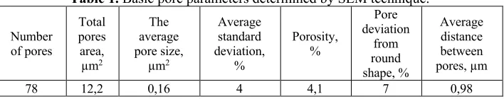
Processing of SEM images using ImageJ has made it possible to estimate the character of pore distribution over the surface, and also to establish the pore diameters on the surface – D = 450 ± 20 nm. The results of determination the pores number, their total area, average size and standard deviation from this value, substrate porosity, as well as pore deviations from the round shape and average pore distance are given in Table 1.
Table 1. Basic pore parameters determined by SEM technique.
Number of pores
Total pores area,
µm2
The average pore size,
µm2
Average standard deviation,
%
Porosity, %
Pore deviation
from round shape, %
Average distance between pores, µm
78 12,2 0,16 4 4,1 7 0,98
The cross-section of the SiO2/Si template (Figure 1c) indicates that the pores have
truncated cone-shaped form. It also allows to determine the internal pore diameter (d), half-pore angle (θ) and silicon oxide thickness after etching (L). The schematically determined pore parameters are shown in Figure 1d. According to the estimation, the pore parameters have the following values: d ~ 160 ± 10 nm and L ~ 440 ± 10 nm, with
θ = 16 °.
To determine the thickness of the silicon oxide layer and, correspondingly, the pore height
L from the experimentally measured ellipsometry data Ye(l), De(l), the following model
of the template structure was used.
Thicknesses, as well as dispersion coefficients, were found by solving the problem of minimizing the objective function of the form:
. (1)
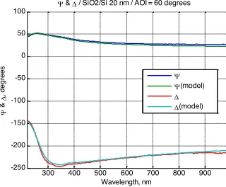
Figure 2 shows the results of comparing the model tothe experimental data.
Fig. 2. The results of comparing physical model of the interaction of a polarized light beam with experimental data obtained from a layered SiO2/Si porous structure.
It can be seen that, the theoretical model is in good agreement with experiment. The pore parameters of SiO2/Si template and the thickness of the oxide layer are correlated with
the etching half-angle θ, given by the energy at the stage of irradiation with SHI [10]. Accordingly, to determine the height, outer and inner diameter of the pores, it is sufficient to know only one parameter in combination with the initial conditions LSiO2 and θ. The
relation between l and other SiO2 pore parameters was determined by geometric
equations:
𝐷 = 2(𝐿&'()− 𝐿),-./'01-2/'01 , (2)
𝑑 = 𝐷 − 2𝐿 · 𝑡𝑔𝜃, (3)
where θ was taken as a constant angle ≈ 16 °.
The results of comparing the thickness of SiO2 using the ellipsometry method determined L = 435 nm. The values of D and d were calculated by the following equations (2-3) and equaled 420 and 171 nm, respectively. The ellipsometry method provides information from a large sample area (the diameter of the observed region is from 10 to 200 μm, depending on the preliminary settings of the equipment). For example, on samples with a pore density of 5×107 cm-2, ~50 pores enter the field of a polarized beam with a size of
200 μm in one measurement. Thus, the ellipsometry makes it possible to determine the averaged pore parameters in one measurement quickly and efficiently, so that to save considerable time during the research. In this case, L represents the average integral characteristic from a large area with an accuracy of up to 1 nm, which is due to the measurement of the relative (amplitude Y(l) and phase shift D(l)), rather than absolute values. One more advantage of ellipsometry compared with the SEM is theabsence of necessity for the partial destruction of the sample (preparation of cross-section).
2 2
1
min m ( e i) ( e i)
i
t t
=
é ù
s=
å
ëy - y + D - D û300 400 500 600 700 800 900 -250
-200 -150 -100 -50 0 50
100 Y
& D / SiO2/Si 20 nm / AOI = 60 degrees
Wavelength, nm
Y
&
D
, d
e
g
re
e
s
Y Y(model) D D(model)
EPJ Web of Conferences 201, 01001 (2019) https://doi.org/10.1051/epjconf/201920101001
4 Conclusions
The silicon oxide templates on silicon are formed by irradiating SiO2/Si substrates with
SHI and their subsequent etching with HF. Using the SEM and ellipsometry, a comparative analysis of the pore parameters of obtained templates has been carried out. It was shown that the results obtained by both methods are in good agreement. Taking into account the simplicity of sample preparation, high precision and the short time of investigation on a large area, these results allow to recommend ellipsometry as a method for parameter express analysis of ion-track SiO2/Si templates with low pore density.
In the future work, in order to develop the proposed approach, it is planned to study a wide range of templates with different pore diameters, oxide layer thicknesses and porosity. The development and presentation of physical model of interaction of polarized light beam with a layered structure of silicon oxide on silicon with high pore density are planned, as well.
Acknowledgments
This work was supported by the Scientific-technical ‘program Technology-SG’ (project number 3.1.5.1) and Belarusian Foundation for Basic Research [project number Ф17М-005] for the financial support.
1. P. Apel, Radiat. Meas. 34 (2001).
2. D.I. Tishkevich, S.S. Grabchikov, S.B. Lastovskii, S.V. Trukhanov, T.I. Zubar, D.S. Vasin, A.V. Trukhaniv, J. Alloys Compd. 749 (2018).
3. D.L. Shimanovich, A.L. Vorobjova, D.I. Tishkevich, A.V. Trukhanov, M.V. Zdorovets, A.L. Kozlovskiy, Beilstein J. Nanotechnol. 9 (2018).
4. F.F. Komarov, Uspekhi Fiz. Nauk. 187 (2017).
5. A. Dallanora, T.L. Marcondes, G.G. Bermudes, P.F.P. Fitchner, C. Trautman, M. Toulemunde, R.M. Papaleo, J. Appl. Phys. 104 (2008).
6. M.E. Toimil-Molares, Beilstein J. Nanotechnol. 3 (2012).
7. E.Y. Kaniukov, E.E. Shumskaya, D.V. Yakimchuk, A.L. Kozlovskiy, M.A. Ibragimova, M.V. Zdorovets, J. Contemp. Phys. (Armenian Acad. Sci.). 52 (2017).
8. A.L. Kozlovskiy, I.V. Korolkov, G. Kalkabay, M.A. Ibragimova, A.D. Ibrayeva, M.V. Zdorovets, V.S. Mikulich, D.V. Yakimchuk, A.E. Shumskaya, E.Yu. Kaniukov, J. Nanomater. 2017 (2017).
9. S.J. Zinkle, J.W. Jones, V.A. Skuratov, MRS Proc. 650 (2000).
10. E.Y. Kaniukov, J. Ustarroz, D.V. Yakimchuk, M. Petrova, H. Terryn, V. Sivakov, A.V. Petrov, Nanotechnology. 27 (2016).
11. D.Yakimchuk, E. Kaniukov, V. Bundyukova, L. Osminkina, S. Teichert, S. Demyanov, V. Sivakov, MRS Commun. 8 (2018).
12. E.Y. Kaniukov, S.E. Demyanov, A.V. Petrov, 18th International Crimean Conference -Microwave & Telecommunication Technology, 2008, pp. 577–578.
13. E.Y. Kaniukov, A.L. Kozlovsky, D.I. Shlimas, M.V. Zdorovets, D.V. Yakimchuk, E.E. Shumskaya, K.K. Kadyrzhanov, Journal of Surface Investigation. 11 (2017).
14. E. Kaniukov, D. Yakimchuk, G. Arzumanyan, H. Terryn, K. Baert, A. Kozlovskiy, M. Zdorovets, E. Belonogov, S. Demyanov, 97 (2017).