R E S E A R C H
Open Access
An orthogonal wavelet division multiple-access
processor architecture for LTE-advanced wireless/
radio-over-fiber systems over heterogeneous
networks
Chinmaya Mahapatra
1*, Victor CM Leung
1and Thanos Stouraitis
2Abstract
The increase in internet traffic, number of users, and availability of mobile devices poses a challenge to wireless technologies. In long-term evolution (LTE) advanced system, heterogeneous networks (HetNet) using centralized coordinated multipoint (CoMP) transmitting radio over optical fibers (LTE A-ROF) have provided a feasible way of satisfying user demands. In this paper, an orthogonal wavelet division multiple-access (OWDMA) processor architecture is proposed, which is shown to be better suited to LTE advanced systems as compared to orthogonal frequency division multiple access (OFDMA) as in LTE systems 3GPP rel.8 (3GPP, http://www.3gpp.org/DynaReport/36300.htm). ROF systems are a viable alternative to satisfy large data demands; hence, the performance in ROF systems is also evaluated. To validate the architecture, the circuit is designed and synthesized on a Xilinx vertex-6 field-programmable gate array (FPGA). The synthesis results show that the circuit performs with a clock period as short as 7.036 ns (i.e., a maximum clock frequency of 142.13 MHz) for transform size of 512. A pipelined version of the architecture reduces the power consumption by approximately 89%. We compare our architecture with similar available architectures for resource utilization and timing and provide performance comparison with OFDMA systems for various quality metrics of communication systems. The OWDMA architecture is found to perform better than OFDMA for bit error rate (BER) performance versus signal-to-noise ratio (SNR) in wireless channel as well as ROF media. It also gives higher throughput and mitigates the bad effect of peak-to-average-power ratio (PAPR).
Keywords:Heterogeneous networks (HetNet); Coordinated multipoint (CoMP); LTE advanced radio over fiber (LTE A-ROF); Orthogonal wavelength division multiple-access (OWDMA) processor; Orthogonal frequency division multiple access (OFDMA); Xilinx vertex 6 FPGA; Bit error rate (BER); Signal-to-noise ratio (SNR); Peak-to-average-power ratio (PAPR)
1 Introduction
The diversity of applications used over the internet has resulted in a demand for increased speed (data rate) over the network and a need for accommodating more users per unit area. This demand has urged research communi-ties to provide greener and more cost-efficient networks. Several research studies have been conducted over the last decade, proposing cost-efficient broadband architectures. Today, next-generation long-term evolution (LTE) systems
using radio signals over optical fibers are evolving towards centralized architectures, as a promising solution to meet the ever-increasing demand for high-speed wire-less connectivity. Centralized architectures, epitomized by micro base stations, femto and picocell base-station/ac-cess-point architectures, and mesh networking solutions have promised to provide several benefits, including re-duced power consumption, enhanced radio spectrum utilization capacity, and diversity of next-generation wire-less communication networks [1].
As radio spectrum is expensive and band-limited, cen-tralized LTE advanced-radio over fiber (ROF) has attracted significant research interest. It focuses on the optimum * Correspondence:[email protected]
1
Department of Electrical and Computer Engineering, University of British Columbia, V6T1Z4 Vancouver, BC, Canada
Full list of author information is available at the end of the article
construction and utilization of the hardware resources to cater an area of high traffic. A typical design uses optical fiber to move analog or digitized radiofrequency (RF) between the central facility and the remote sites [2]. Choosing optical fiber over conventional coaxial cables enables the usage of the enormous bandwidth provided by the fiber as well as almost error-free transmission for short ranges in a metro area network (MAN). Software-defined radio (SDR) provides efficient, cost-effective and easy-to-handle deployment architecture for the LTE A-ROF sys-tem. It follows a normal server/multi-client IT network and provides flexibility in architecture deployment. It also provides big savings of operational and infrastructure cost for service providers.
In the current LTE and Wi-Fi systems, orthogonal frequency division multiple-access (OFDMA) is the tech-nology of choice [3]. OFDMA uses inverse fast Fourier transform (IFFT) at the transmitter and fast Fourier trans-form (FFT) at the receiver and allocates fixed resources to users for a given set of operating parameters. Despite its several advantages, if coupled with other components of the LTE A, the use of OFDMA increases the cost and utilization overhead of system resources. Moreover, it suffers from large implementation complexity, requiring a fixed allocation of resources to all the users, regardless of the present traffic as well as a high peak-to-average-power ratio (PAPR) [4].
Orthogonal wavelet division multiple access (OWDMA) has been proposed as a viable alternative to OFDMA in communication systems. Previous work concentrated on digital video broadcast, and results were only plotted for the BPSK modulation scheme [5,6]. Raajan et al. [7] pro-vided bit error rate (BER) performance graphs for all the wavelets and modulation schemes, but no hardware archi-tecture was provided for the proposed system. Similarly, Tao et al. [8] and Liew et al. [9] analyzed orthogonal wave-let division multiplexing (OWDM) for signaling over wideband linear time-varying channels (LTV) but, again, did not provide any architecture for deployment. 1-D orthogonal wavelets have been used [10-14] for image processing applications.
The paper is organized in sections, where Section 3 pro-vides a brief description of previous work, the definition of wavelet transform, and reasons for choosing 9/7 Daube-chies lifting scheme for evolving the architecture. Section 4 describes the proposed OWDMA processor architecture and explains the different building blocks. In Section 5, pipelining is introduced in the architecture to reduce power consumption. Section 6 presents the synthesis and com-parison results of resources and timing with other similar architectures. Section 7 gives the performance comparison for OWDMA and OFDMA, based on quality of constraint (QOS) metrics for LTE A-ROF systems. Finally, conclu-sions are offered in Section 8, followed by references.
2 Key contributions
A sequential output-based parallel processing (SBPP) architecture for OWDM was proposed and evaluated for BER and PAPR [15]. Its deployment in LTE A future 3GPP rel.10 and above requires that its structure should be flexible enough to adapt according to channel condi-tions to different values of transform size in order to ser-vice uniformly the same number of users. The structure needs to accommodate both forward and inverse opera-tions through a common control input. The architecture should be power efficient, easily controllable through a single control and should have input-output ports matching with other system sub-blocks that will satisfy the timing requirements of the whole system. Moreover, it is important for it to offer improved performance in terms of spectral efficiency (throughput), quality of service (bet-ter BER at the same signal-to-noise ratio (SNR)) and should fit well in radio-over-fiber systems. In this paper, an OWDMA architecture is developed that has signi-ficantly better performance, is easy to deploy, and con-sumes fewer resources than similar architecture available in the literature.
Analyzing the approaches described in [5-9] gives insight about the extensive research performed on the various solution approaches to problems of LTE OFDMA systems and provides proof that orthogonal wavelets are a better and viable alternative to the existing wireless sys-tems. Although the analysis and evaluations were done for BER and PAPR, it lacks in a unified system implementa-tion, resource analysis, and thorough performance eva-luation for current LTE systems. Our major contribution in this paper is to deal with these shortcomings in the present knowledge and present an overall system level so-lution. Moreover, we also provide performance analysis for optical fiber medium.
3 Orthogonal wavelet division multiplexing Fast fluctuations in the time domain or frequency-specific information in the time domain can only be revealed through a time/frequency analysis. The wavelet transform maps a time function into a two-dimensional function of ‘a’(the scale) and‘τ’(the translation) of the Wavelet func-tion along the time axis [16,17]. The continuous waveform transform (CWT) of a signals(t) has been defined as
3.1 Formulation of OWDM from the 9/7 filter using lifting From the CWT, it is possible to construct the discrete wavelet transform (DWT) and the inverse DWT) from banks of matched high-pass filters (HPF) and low-pass filter (LPF) [18]. Single carrier systems tend to have high bit rates but low frequency resolution, whereas OFDM has many sublevels, each transferring at a low bit rate. Since the wavelet transform contains both time and frequency information, it is possible to effectively send different data rates in different sublevels, according to channel conditions. When considering the DWT, there are a number of mother wavelet families that need to be evaluated. To replace OFDM systems in a multipath environment having carrier and symbol interference, the wavelets need to be orthogonal and periodical. Also, the realization using discrete structures is important for purpose of implementation. Therefore, only three families of wavelet satisfy all the abovementioned constraints: Daubechies, Symlet, and Coiflet [19].
Figure 1 presents a comparison of signal-to-noise ratio vs. bit error rates for the Symlet 1, Coiflet 2, and Daubechies 2 similar-order filters [19]. It can be seen that the least resilient wavelet family is the Symlet, followed by the Coiflet, then the Daubechies, which appears to be better suited for implementation.
The lifting scheme is used for the development of the architecture for a 9/7 Daubechies 1-D wavelet filter with two stages of lifting (N= 2), i.e., predict1 and update1, followed by predict2 and update2 in a second stage, followed by scaling [20,21]. The basic idea of the lifting scheme is first to compute a trivial wavelet (or lazy wavelet transform) by splitting the original 1-D signal into odd-and even-indexed subsequences odd-and then modify their values using alternating prediction and updating steps
[22,23]. The lifting algorithm consists of the following three steps:
Split step
The original signal, X(n), is split into odd and even samples (lazy wavelet transform).
Lifting step
This step is executed as N sub-steps (depending on the type of the filter), where the odd and even samples are alternatingly filtered by the prediction and update filters.
Scaling step
AfterNlifting steps, scaling coefficientsKand 1/Kare applied, respectively, on the odd and even samples, in order to obtain the low-pass band and the high-pass sub-band.
Orthogonal wavelet division multiple access (OWDMA) is a system, in which the wavelet domain is used to separ-ate the sub-band components in the same way as OFDMA. The big difference between OFDMA and OWDMA is that in OFDMA, the FFT performs sub-band decomposition with a specific number of sub-bands at well-defined inter-vals, while OWDMA may dynamically allocate the number of sub-bands and the bandwidth of each [24].
4 OWDMA processor architecture for LTE A and LTE A-ROF
From the SBPP-OWDM scheme presented in the previ-ous section, it is found that the final scaling and dilation
coefficients are interdependent on predict and update outputs at each stage; thus, there is a delay and it also affects throughput. The structure requires two update and predict blocks to be implemented. OWDMA scheme requires that the structure should be flexible enough to adapt to different values of N, according to the channel conditions. The structure needs to accommodate both forward and inverse operations through a common con-trol. The multiplicative coefficients for the filter need to be stored in a hardware-friendly format which will reduce the number of multiplication operations. Thus, a new OWDMA processor architecture has been developed that caters to all the requirements of a multiple-access system mentioned above. Moreover, parallelism is exploited in the architecture, along with pipelining, to formulate an efficient, low-power, and resource-friendly processor.
Predict and update block1 and predict and update block2 are combined together along with the scaling. In the forward operation, the wavelet coefficients for odd and even samples are calculated using (2) and (3). The odd values are calculated using a structure implementing a 9-tap finite impulse response (FIR) filter, and the even values are found out with a 7-tap FIR filter structure, as shown in Figure 2. Odd index wavelet coefficients first, third, n−3, and n−1, and even index wavelet coeffi-cients second, n−2, andnth have adjusted input values fed using the symmetry property of the filter. The values ofkbefore the first value‘X[1]’and after the last value ‘X[N]’are replaced by their symmetric values by usingx [k] =x[k+ 2i], where itakes the value−k+ 1 w.r.t to the input indexkat the left side of the axis, and it takes the
value N−k at the right side of the axis. The FOC(j)
and FEC(l) are forward odd and even filter coefficients,
respectively, wherej= 1,2…9 andl= 1,2….7.
YEVEN½ ¼N FECð Þ 1 X N½ −3 þFECð Þ 2 X N½ −2 þFECð Þ 3 X N½ −1 þFECð Þ 4 X N½ þ þFECð Þ 5 X N½ þ1 þFECð Þ 6 X N½ þ2 þFECð Þ 7 X N½ þ3;fN¼EVENg
ð2Þ
YODD½ ¼N FOCð Þ 1 X N½ −4 þFOCð Þ 2 X N½ −3 þFOCð Þ 3 X N½ −2 þ þFOCð Þ 4 X N½ −1 þFOCð Þ 5 X N½ þFOCð Þ 6 X N½ þ1 þ þFOCð Þ 7 X N½ þ2 þFOCð Þ 8 X N½ þ3 þFOCð Þ 9 X N½ þ4;fN¼ODDg
ð3Þ
In the inverse operation, the wavelet coefficients for odd and even samples are calculated using (4) and (5). The odd values are calculated using a structure imple-menting a 7-tap FIR filter, and the even values are found with a 9-tap FIR filter structure. Odd index wavelet coef-ficients first, third, and n−1, and even value wavelet coefficients second, fourth, n−2, andnth have adjusted input values from symmetry in a similar way as descri-bed in the previous paragraph for the forward operation. The boundary conditions are formulated using a state machine control logic implementation elaborated in the control unit section. The IOC(l) and IEC(j) are inverse
odd and even filter coefficients, respectively, where j= 1,2…9 and l= 1,2….7.
XEVEN½ ¼N IECð Þ 1 Y N½ −4 þIECð Þ 2 Y N½ −3 þIECð Þ3 Y N½ −2 þ þIECð Þ 4 Y N½ −1 þIECð Þ5 Y N½ þIECð Þ 6 Y N½ þ1 þ þIECð Þ7 Y N½ þ2 þIECð Þ 8 Y N½ þ3 þIECð Þ9 Y N½ þ4;fN¼EVENg
ð4Þ
XODD½ ¼N IOCð Þ 1 Y N½ −3 þIOCð Þ 2 Y N½ −2 þIOCð Þ3
Y N½ −1 þIOCð Þ 4 Y N½ þ þIOCð Þ5
Y N½ þ1 þIOCð Þ 6 Y N½ þ2 þIOCð Þ7
Y N½ þ3;fN¼ODDg
ð5Þ
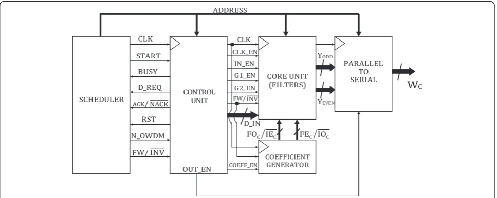
The proposed OWDMA processor consists of a core unit to multiply filter coefficients with delayed input, accumulate with previous values, and compute the wave-let coefficients. Its control unit controls which coeffi-cients are to be applied at the complex multiplier input. A coefficient generator unit reads the appropriate coeffi-cients from memory. The OWDMA unit acts as slave to a master scheduler unit that feeds it with clock, address, input data, and variables. Figure 3 shows the high-level architecture of the OWDMA processor unit with the scheduler. The architecture is a two-parallel structure due to simultaneous calculation of odd and even data. The scheduler and the three major units of the proposed system, namely, the core unit, control unit, and the coef-ficient generator unit, are discussed below.
4.1 Scheduler
The proposed OWDMA processor can be interfaced with the scheduler, according to the scheme presented
Figure 3. In this scheme, the scheduler communicates with the OWDMA processor using a set of dedicated hand-shaking signals. The scheduler acts as the master, sets the address of the processor, and provides clock to it (CLK). First, the scheduler requests the control unit block to initiate a new transform using the START sig-nal. The controller unit sets the BUSY signal low, if it is ready to start the process for the new transform, or high, if it is in the middle of an already continuing process. When the controller is ready, it sends a data request (D_REQ) signal to the scheduler, which then responds with the input data. If the controller correctly gets the input, it sends an acknowledgement (ACK) signal; other-wise, it sends NACK , and the scheduler retransmits. Along with the data input, it sends the information for the size of OWDM (N_OWDM) as well as the forward/ inverse operation ( FW=INV ) signal. The OWDMA pro-cessor uses the RST signal to indicate the end of data, when it completes the transform. At the same time, it sets the BUSY signal low to indicate to the scheduler that it is ready to start a new transform.
4.2 Core unit
The core unit consists of two FIR filter units. One is 9-tap and the other is a 7-tap, as shown in Figure 2. They both have CLK, CLK_EN, IN_EN, G1_EN, G2_EN, D_IN, and FW=INV, as common inputs, andYODDandYEVENas the odd and even filter outputs. The only difference is the inputted coefficients for the multiply and accumulate units inside the FIR filters. The FOC(1…9), IEC(1…9) are
the coefficient inputs for the 9-tap filter block, and FEC
(1…7), IOC(1…7) are coefficient inputs for the 7-tap filter
block. These coefficients are explained in more detail in Section 4.4. The CLK input counts from 0 toN+ 4 and
then gets reset. The extra 5 clock cycles after the normal N-cycles are for flushing the output to 0. D_IN is the data input. IN_EN is enable signal for data input. G1_EN and G2_EN are enable signals for switches that switch input gates and are enabled by the control logic. FW=INV signal is for forward (a‘0’) and inverse operation (a ‘1’). The outputs of both filters are fed to a parallel-to-serial converter block that downsamples the data and rearranges the coefficients to give the final coefficientsWC. It has an
OUT_EN (output enable) signal to start calculating the output WC (the wavelet coefficients). Figure 4 shows all
the logic signals in a timing diagram.
4.3 Control unit
The control unit consists of two separate logic units for forward and inverse computation and is implemented using a finite state machine having five states: S0, S1, S2, S3, and S4. It toggles on the positive CLK edge input, and at each state, the output controls IN_EN, G1_EN, G2_EN, OUT_EN, FW/ INV, _COEF_EN (0/1), and FW=INV. The FW=INV signal controls which control the logic unit is to be used (forward or inverse). G1_EN and G2_EN are gate control switches that switch inputs for the delay registers at the boundary conditions.
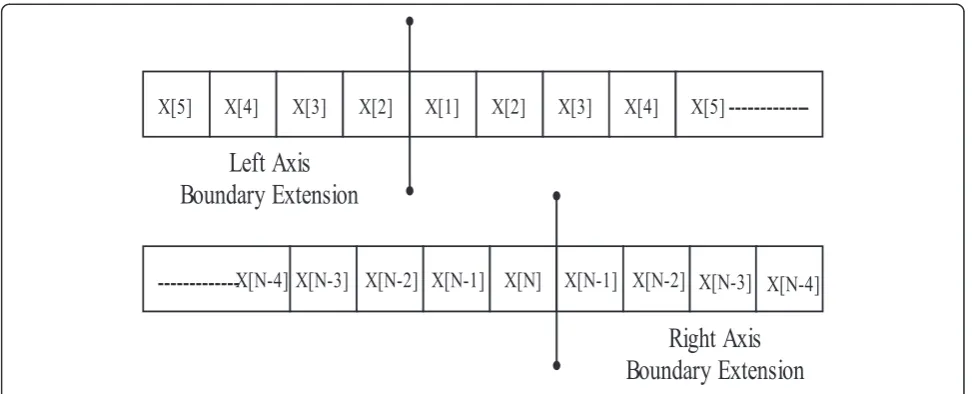
The input value has to be symmetrically extended at the boundaries to avoid distortion.‘X[1]’ is the first in-put value and no previous value is available. Using the symmetric property of the lifting scheme [20] as shown in Figure 5, the next input value ‘X [2]’ is extended to the left of ‘X [1]’and is used to perform the filter oper-ation. Similarly, at the end of the row, the input value ‘X[N]’ is the last one. By copying the input value‘X[N-1]’ to the right of ‘X[N]’, the boundary condition at the right end can be satisfied. The control logic is shown in Figure 6. At the positive edge count value of 4, G1_EN is enabled for 1 clock cycle. G2_EN is enabled atnth clock value. Output is calculated starting from fifth clock count to (n+ 4)th count and then everything resets back to state S0.
4.4 Coefficient generator unit
The coefficient generator block is a memory block that contains the odd and even filter coefficients to be multiplied during forward/inverse operation. Providing the appropriate constant to the multiplier, it implements the desired multiplication. The width of the multi-pliers is determined by the accuracy of the constants and the data path bitwidth. The drawback of the above implementation is that the multipliers occupy a great amount of area and restrict the throughput of the processing unit. Using shift-add operations to replace the multiplications with constants optimizes the above implementation and results in an improved processing block.
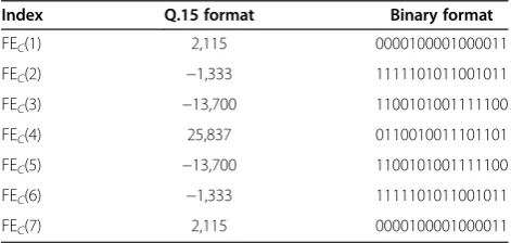
To perform shift and add operations, coefficients are converted in two's complement Q.15 format. That is, they are shifted 15 bits to the left and converted to their respective two's complement binary value. The filter constants are quantized, taking in account the number of bits with value ‘1’, in their positive representation. That is because each‘1’yields a term to be summed. For example, the sets of odd and even coefficients for the forward path are shown in Tables 1 and 2, respectively, similarly, the coefficients for the reverse path can be defined.
5 Pipelining the parallel architecture
Power dissipation is a major drawback of the system in the downlink and especially the uplink of a LTE A net-work. In the proposed OWDMA processor architecture, pipelining the stages of the 9-tap and 7-tap filters, along with the two-stage parallel structure, can help save in power budget. The saved power can be used to accom-modate more number of users or increase the range of the system. Pipelining reduces the effective critical path by introducing latches along the critical data path. The critical path (or the minimum time required for pro-cessing a new sample) is limited by 1 multiply and 8
add times in the 9-tap filter structure and 1 multiply and 6 add times in the 7-tap filter structure of the OWDMA processor, respectively, as shown in Figure 2. Thus, the ‘sample period’ is given by (6) and (7), where Tsample (9-tap) and Tsample (7-tap) are the sampling fre-quencies of the respective filters
Tsampleð9−tapÞ≥TMþ8TA ð6Þ
Tsampleð7−tapÞ≥TMþ6TA ð7Þ
Pipelining is accomplished by introducing 14 and 10 additional latches in the feed-forward path of the 9-tap and the 7-tap filter structure, respectively, thereby
reducing the critical path to TM+TA for both filters. In an M-level pipelined system, the number of delay elements in any path from input to output is (M−1) greater than that in the same path in the original se-quential circuit. Thus, we apply eight-level pipelining to the 9-tap filter circuit and six-level pipelining to the 7-tap filter circuit. When the sample speed does not need to be increased, this can be used for lowering the power consumption. The power dissipation (PCMOS) in any circuit depends on the total capacitance Ctotalof the CMOS logic, the supply voltage VCC, and the clock fre-quencyf. The total power depends on static and dynamic power consumption:
Figure 5Symmetric boundary extension of input data.
PCMOS¼CtotalV2CCf;f ¼1=Tseq ð8Þ
With increase in propagation/gate delay, leakage current decreases, thereby reducing the static power consumption of the system [25]. The propagation delay (Tpd) depends on the charging capacitance Ccharge in a clock cycle and the difference (VCC−Vt)2, whereVtis the threshold
Applying pipelining reduces the capacitance to be charged/discharged in one-clock period, while the in-herent parallel processing allows for increasing the clock period for charging/discharging the original cap-acitance. In an L-parallel system (L= 2 in our case), the clock period of the circuit is increased to LTpd. This implies that the supply voltage can be reduced to βVo (0 <β< 1). Hence, the power consumption, compared with the original system, is reduced by a factor β2. The propagation delay of the L-parallel, M-pipelined filter is obtained as
Finally, we can obtain the following equations to compute β and power dissipated in OWDM circuit, respectively
6 Performance results and comparisons
6.1 Synthesis of the proposed architecture and resource utilization
In order to evaluate the performance of the architecture, it is required to make use of certain metrics that characterize the architecture in terms of the hardware resources used and the computation time. The hardware resources used for filtering are measured by the number of multipliers an number of adders, while those used for the storage of data and filter coefficients are measured by the number of registers. In general, the computation time is technology dependent. However, a metric that is technology independent and can be used to determine the computation time (T) is the number of clock cycles (NCLK) elapsed between the first and the last samples inputted to the architecture. Assuming that the clock period is Tc, the total computation time can then be obtained asT=NCLK×Tc.
To validate the circuit design based on the proposed architecture, the implementation is done on a test bed that includes one central processor with multiple dis-tributed antenna nodes and multiple mobile stations. The test bed operates in the 2.4-GHz ISM band for its license-exempt convenience. The central processor con-sists of RF front ends with 20- to 80-MHz bandwidth, a number of 125 ~ 250-MHz 14-bit ADC/DACs mounted on the latest Xilinx Virtex-6 FPGA digital signal process-ing (DSP)/FPGA processprocess-ing unit (San Jose, CA, USA) to pre-process data samples. All the carry propagation adders of the architecture have a 16-bit word length and use a structure that combines the skip and carry-select adders [26]. The FPGAs inside the platforms are XC6VLX75T-2, which is capable of operating at a clock frequency of 650 MHz at supply voltage of VCC= 2.5 V and quiescent voltage ofVt= 1.5 V. The resources utilized by the FPGA implementation in terms of the numbers of configuration logic block (CLB) slices, flip-flop slices, DSP 48's, input/output blocks (IOBs), and block RAMs (BRAMs) are given in Table 3.
The implemented circuit is found to perform well with a clock period as short as 7.036 ns (i.e., a maximum clock frequency of 142.13 MHz) for a transform size of Table 1 Forward odd coefficients
Index Q.15 format Binary format
FOC(1) −1,240 1111101100101000
FOC(2) 781 0000001100001101
FOC(3) 9,956 0010011011100100
FOC(4) −16,358 1100000000011010
FOC(5) 30,031 0111010101001111
FOC(6) −16,358 1100000000011010
FOC(7) 9,956 0010011011100100
FOC(8) 781 0000001100001101
FOC(9) −1,240 1111101100101000
Table 2 Forward even coefficients
Index Q.15 format Binary format
FEC(1) 2,115 0000100001000011
FEC(2) −1,333 1111101011001011
FEC(3) −13,700 1100101001111100
FEC(4) 25,837 0110010011101101
FEC(5) −13,700 1100101001111100
FEC(6) −1,333 1111101011001011
N= 512. By replacing the values ofVCC,Vt, L, andM in (18) and (19), it can be found out that the power con-sumption on the chip on which the circuit is implemented is reduced by a factor of (1/9). The new power usage is only 143 mW per antenna.
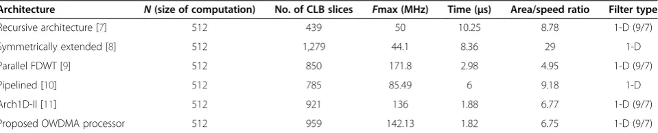
6.2 Comparison with other architectures
The proposed OWDMA architecture is compared next with various 1-D wavelet architectures, as well as with available commercial OFDMA chips. Computation time (T), CLB slices or area occupied on FPGA, maximum clock frequency and area/speed ratio are some of the key performance metrics that are compared. Table 4 gives the comparison results between different 1-D wavelet architectures present in the literature. For even compari-son,N= 512 is taken as the size of the input data in all architectures. It can be inferred from the table that although our proposed architecture consumes a few more hardware resources as compared to recursive architecture [10], parallel FDWT [12], pipelined [13], and Arch1D-II [14], it significantly performs better in terms of maximum clock frequency and computation time. It is also seen that the area to speed ratio is the second lowest for our archi-tecture. Although the parallel FDWT implementations [12] present a better area/speed ratio, high computation times make them unsuitable for high-speed applications.
Current advanced 4G systems deploy OFDMA archi-tecture. So, it becomes imperative to compare our proposed OWDMA processor architecture with the state-of-the-art implementation. The OFDMA core uses the Radix-4 and Radix-2 decompositions for computing the discrete Fourier transform (DFT) [27,28]. When using the Radix-4 decomposition, the N-point FFT consists of log4 (N) stages, with each stage containingN/4 Radix-4 butter-flies. Point sizes that are not a power of 4 need an extra
Radix-2 stage for combining data. AnN-point FFT using Radix-2 decomposition has log2 (N) stages, with each stage containingN/2 Radix-2 butterflies. The comparison between the two architectures is depicted in Table 5. It can be seen that there is at least 90% improvement in the computation time when OWDMA core is used as opposed to OFDMA core for a 10% increase in DSP resources on the FPGA, whereas the total area occupied on FPGA remains comparable with the respectiveN-point computation. Furthermore, it has been shown [6] that the OWDMA which implements wavelet transforms has a complexity of O(N), as opposed to the OFDMA that contains FFT operations and has complexity of O (Nlog2N).
7 Quality comparison in 4G LTE A/LTE A-ROF system
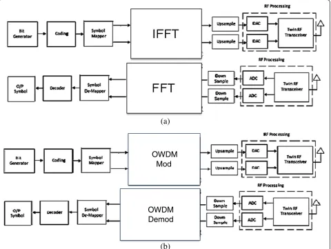
In any communication system, BER versus SNR and spectral efficiency (throughput) are standard quality of service (QoS) parameters, which give a measure of system performance. Therefore, the proposed OWDMA architecture has been compared to existing OFDMA architectures in 4G LTE A systems with respect to the above two QoS parameters. Figure 7 shows the difference between the two implementations with respect to a prac-tical system perspective. As can be seen in Figure 7a,b, the difference is in the IFFT/FFT blocks of OFDMA that are replaced by OWDM modulator/OWDM demodulator block. The number of samplesNOFDMis same asNOWDM that is modulated and demodulated input/output in the respective paths. The inherent processing is similar for both OFDM and OWDM, the only difference being the way the samples are treated in the respective processors. So, there is no need to make any significant changes to the overall processing samples. Only replacing the IFFT/ FFT blocks of OFDMA with that of OWDM modulator/ OWDM demodulator will serve our purpose.
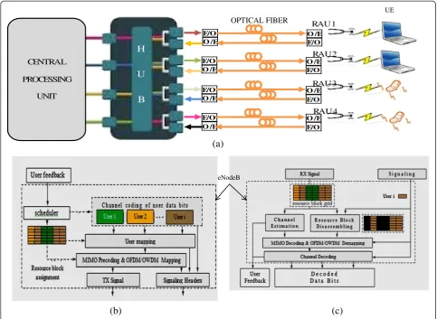
Figure 8a gives an overview of the proposed central-ized CoMP system based on an existing LTE backbone with fiber connectivity. The system consists of a central processing unit (CPU) that contains the Xilinx FPGA and DSPs for all the data processing for uplink and downlink. There are four separate processing modules inside the CPU model in Figure 8a, each having transmit
Table 4 Comparison between various 1-D architectures
Architecture N(size of computation) No. of CLB slices Fmax (MHz) Time (μs) Area/speed ratio Filter type
Recursive architecture [7] 512 439 50 10.25 8.78 1-D (9/7)
Symmetrically extended [8] 512 1,279 44.1 8.36 29 1-D
Parallel FDWT [9] 512 850 171.8 2.98 4.95 1-D (9/7)
Pipelined [10] 512 785 85.49 6 9.18 1-D
Arch1D-II [11] 512 921 136 1.88 6.77 1-D (9/7)
Proposed OWDMA processor 512 959 142.13 1.82 6.75 1-D (9/7)
Table 3 FPGA resource summary for OWDMA
(Tx) and receive (Rx) data processing capability. The four modules are connected to a 4 × 4 hub that, in turn, is connected to a RF switch, capable of switching in Tx and Rx directions. The transmit and receive directions have an electrical-to-optical convertor (laser diode) to convert from electrical to optical signal to be transmitted via the fiber to a remote antenna unit (RAU), located at
different places in a cell site. The laser diode is modulated by the RF signal in the downlink path. The resulting intensity-modulated optical signal is then transmitted through the single-mode fiber towards a photodiode. The received optical signal is converted to RF signal (optical-to-electrical convertor) by direct detection through a PIN photodetector. The signal is then amplified and radiated Table 5 Comparison of resource utilization for OFDMA and OWDMA processors
Technique Architecture N(size of computation)
No. of CLB slices
No. of LUT slices
BRAM DSP slices
Time (μs)
OFDMA processing R2 256 842 650 3 3 4.18
R2L 1,000 1,025 839 3 3 31.58
R2 1,106 882 3 6 18.63
R2L 2,000 1,137 882 5 3 66.74
R2 1,082 952 5 6 39.41
Proposed OWDMA processing Parallel and pipelined 256 614 355 3 32 0.91
Parallel and pipelined 1,000 1,338 1,042 3 32 3.61
Parallel and pipelined 2,000 1,160 848 5 32 7.26
(a)
(b)
OWDM
Mod
OWDM
Demod
by the antenna. The optical fibers cover in practice a dis-tance of few hundred meters to a few kilometers, enough to cover a building or a small area. The RAU is a passive unit containing only optical to electrical convertor and amplifier and a RF antenna at the 2.4/5-GHz band to transmit or receive radio signals. The RAUs are relatively close to the user equipment, generally within few hundred meters. So, an International Telecommunication Union (ITU) pedestrian multipath channel with Doppler fre-quency fd= 5 Hz is chosen for simulations.
Figure 8b,c shows the transmitter and receiver units, respectively, of the proposed architecture. In the first step of the transmitter processing, the user data are generated, depending on the previous acknowledgement (ACK) signal. If the previous user data transport block (TB) was not acknowledged, the stored TB is retransmitted using a hybrid automatic repeat request (HARQ) scheme. Then, a cyclic redundancy check (CRC) is calculated and appended to each user's TB. The data of each user are inde-pendently encoded using a turbo encoder with quadrature
permutation polynomial (QPP)-based interleaving [29]. Each block of coded bits is then interleaved and rate-matched with a target rate, depending on the received channel quality indicator (CQI) user feedback. The encod-ing process is followed by data modulation, which maps the channel-encoded TB to complex modulation symbols. Depending on the CQI, a modulation scheme is selected for the corresponding resource block. Modulation schemes used for downlink-shared channel (DL-SCH) here are QPSK, 16-QAM, and 64-QAM. The modulated transmit symbols are then mapped to a multiple-input and mul-tiple-output (MIMO) precoding matrix. The optimum precoding matrix is selected from a code book, depending on the pre-coding control information (PCI) that is fed back from the user equipment (UE) to the transmit-ter. Finally, the individual symbols to be transmitted are mapped to the resource elements. Downlink refer-ence symbols and synchronization symbols are also inserted into the OFDM/OWDM time-frequency grid. The assignment of a set of resource blocks (RBs) to CENTRAL
PROCESSING
UNIT
E/O O /E
E/O O /E
E/O O /E
E/O O /E
O /E E/O
O /E E/O
O /E E/O
O /E E/O
H
U
B
RAU 1
RAU 2
RAU 3
RAU 4 OPTICAL FIBER
UE
(a)
eNodeB
UEs is carried out by the scheduler based on the CQI reports from the UEs.
The receiver structure is shown in Figure 8c. Each UE receives the signal transmitted by the evolved node B (eNB) and performs the reverse physical-layer processing of the transmitter. First, the receiver has to identify the RBs that carry its designated information. The estima-tion of the channel is performed using the reference sig-nals available in the resource grid. Based on this channel estimation, the quality of the channel may be evaluated, and the appropriate feedback information calculated. The channel knowledge is also used for the demodu-lation and soft decoding of the OFDM/OWDM signal. In case of MIMO, a MMSE decoder is used. Finally, the UE performs HARQ combining and channel de-coding. In order to cut down the processing time after the end of every turbo iteration, a CRC check of the decoded block is performed and, if correct, decoding is stopped.
The path from UE to RAU, i.e., the uplink uses single carrier-frequency division multiple access (SC-FDMA) as OFDM, has high PAPR. High PAPR requires expen-sive and inefficient power amplifiers with high require-ments on linearity, which increases the cost of the user terminal and also drains the battery faster. Since OWDM has better PAPR, it can be used in the uplink as well.
7.1 Bit error rate comparison
Using the above system model, standard QoS parameters BER and throughput have been compared for OFDM and OWDM architectures. In addition, a performance evaluation of radio over single-mode fiber system using coded OFDM and OWDM and the relation of fiber length with BER is discussed. A comparison is also drawn be-tween peak-to-average-power ratio in the two systems.
Figure 9a,b,c shows the simulation results for bit-error-rate versus signal-to-noise ratio for OWDMA/OFDMA systems for different modulation formats. Table 6 shows the parameters used for the simulations. The plots are drawn for modulation schemes of QPSK, 16-QAM, and 64-QAM for an ITU-defined extended pedestrian A model (EPA) with Doppler frequency fd= 5 Hz. The size of transform for both the architectures is taken as 1,024, for a total of 50 resource blocks at 20-MHz bandwidth. Comparisons are drawn taking both un-coded and rate-1/2 turbo-un-coded OWDMA/OFDMA systems. We can infer from the graphs that OWDMA performs better than OFDMA for both coded and un-coded schemes. At QPSK modulation, as in Figure 9a, OWDMA shows a performance improvement close to 1.5 dB, which increases to nearly 2.5 dB for 64-QAM modulation, as shown in Figure 9c. The gain in SNR can
be used to either increase reach or accommodate more users.
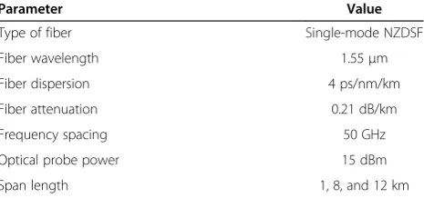
The relation of optical fiber length with BER in terms of performance (SNR of radio-over-fiber) is shown in Figure 9d. Table 7 defines the simulation parameters for the optical link. The SNR of radio-over-fiber is de-fined as the ratio of probe power (PFIBER) of the fiber and the total noise in the ROF system. Total noise of the ROF system is the sum of additive white Gaussian noise (AWGN) plus the fiber nonlinearities and it passes through an ITU multipath fading channel (EPA channel), as defined in the previous case. The SNR of ROF is given by (13), where h is the radio channel coefficient, and NAWGN and NFIBER-NL are the AWGN noise and degradation from fiber nonlinearities, respectively.
We find that there is no significant degradation on the BER performance until the fiber length becomes 12 km, due to considerable modal dispersion. OWDMA shows slightly better performance as compared to the OFDMA system. This shows that the OWDM-ROF system en-sures high service availability over long distances up to 8 km, which came in accordance with standard dis-tances between the indoor (baseband) and outdoor (radio) units.
7.2 Throughput of the OWDMA system
In this section, we compare the throughput of the OWDMA systems as compared to that of the OFDMA systems. In a fading system, the capacity of a massive MIMO system is given by [30]
assumed to be. So, the discrete sampled received signal, r[n], at the output of the channel can be written as
r n½ ¼X
L−1
l¼0
h l½ x n½ þv n½ ð15Þ
It is well known that multiplication in the DFT domain corresponds to the circular convolution in the time do-main. In order to achieve circular convolution using linear convolution, we must add a prefix that is the‘cyclic prefix’ onto the transmitted signal. This cyclic prefix makes the linear convolution appear as a circular convolution and represents a loss in the achievable data rate that becomes significant in the highly fading channels. But in the case of OWDM that uses wavelet transform, the operations
involve shift and multiply operations with filter coeffi-cients. The shift by two for subsequent pairs of rows pro-duces a downsampling operation within the matrix transformation and also makes the matrix orthogonal and circulant [31]. Therefore, a cyclic prefix is not required in the case of OWDM. This gives a significant throughput advantage particularly in highly dispersive channels.
Figure 10 shows the throughput (Mb/s) versus SNR in decibels with values of M (RAUs) ranging from 1 to 4 for OWDM and OFDM systems. Shannon's limit for the capacity at different M is also drawn to show the upper bound. The red circles depict the throughput for OWDM/ OFDM at a particular modulation scheme and SNR. It is found that the OWDM system achieves better throughput at same channel conditions putting less burden on the
Table 6 Simulation parameters
Parameter Value
Channel bandwidth 20 MHz
Modulation schemes QPSK, 16-QAM, 64-QAM
Multiple access architectures OWDMA/OFDMA
N(size of computation) 1,024
Error control code Rate-1/2 turbo codes
Channel model ITU extended pedestrian A model (EPA)
withfd= 5 Hz
Table 7 Fiber parameters in optical link
Parameter Value
Type of fiber Single-mode NZDSF
Fiber wavelength 1.55μm
Fiber dispersion 4 ps/nm/km
Fiber attenuation 0.21 dB/km
Frequency spacing 50 GHz
Optical probe power 15 dBm
Span length 1, 8, and 12 km
overall resources in terms of modulation used, at a given SNR. For instance, OWDM with QPSK provides 25% better throughput performance as compared to OFDM with 16-QAM between 12- and 14-dB SNR. Data rates up to 760 Mb/s can be achieved using OWDM systems, and the results are very close to Shannon's limit. Thus, OWDM is not only a more efficient system than OFDM but a system that performs close to Shannon's limit.
7.3 Peak-average-to-power ratio
PAPR appears to be a main disadvantage of OFDM. In this paper, we show that PAPR performance in OWDMA is better than that of the OFDMA systems. PAPR depends on the bandwidth efficiency of the system. The problem of high PAPR is usually associated with OFDM because it is much easier to reach high bandwidth efficiency for OFDM. There exist a large number of publications in literature devoted to the PAPR problem in OFDM, mostly claiming only a slight improvement on the exiting architecture. The
results of tests indicate that OWDM is the ideal candidate to solve the existing PAPR issues and still deliver high bandwidth efficiency. Our PAPR simulation and analysis is carried out based on its complementary cumulative distri-bution (CCD). So, for a given PAPR0(dB), the percentage of combinations that guarantee (PAPR > PAPR0) is a mean-ingful criterion for analysis. In general, the PAPR of wavelet coefficients coming out is defined in (16) as the ratio be-tween the maximum instantaneous power and its average power, where E[WC(t)]2 is the average power of WC(t)
(wavelet coefficients).
PAPR dBð Þ ¼10 log10 maxjWCð Þt j
2
E Wj Cð Þt j2
" #
ð16Þ
The PAPR performance metric we consider is the com-plementary cumulative distribution function (CCDF), which is plotted as in Figure 11. The OWDMA system provides
Figure 10Signal-to-noise ratio versus throughput (spectral efficiency) for OWDMA and OFDMA systems at different values ofM.
reduced PAPR of around 2 dB, which is favorable for RF amplifier operation as compared to OFDMA systems.
8 Conclusion
In this paper, we have developed a flexible, hardware-friendly, and low-power OWDMA architecture design for deployment in ROF systems having LTE-advanced configuration. The key contribution of the paper is the architecture derived for a LTE A-ROF system with an interface of input and output ports that can replace the OFDMA block offering added benefits.
We first derived an architecture based on previous 9/7 lifting scheme wavelet filters. The computation of the method is described using filters, controller, and parallel-to-serial units. The scheduler is also implemented for easy interfacing of the sub-block with other blocks of the system. The architecture is validated on a centralized processor having Xilinx Virtex-6 FPGAs at N= 512. We compare our architecture with various other 1-D 9/7 wavelets available in the literature as well with exist-ing OFDMA implementations. We also compute the qual-ity parameters BER, throughput, and PAPR for OWDMA and compare them with the existing OFDMA systems.
We found that our architecture runs at a speed of 142.13 MHz, consuming only 143 mW of power per antenna. It is better, in terms of resource consumption, as compared to other similar 1-D 9/7 implementations. We also found that it is also significantly better than OFDMA systems in terms of resource utilization and BER, throughput, and PAPR performance for ROF sys-tems. Hence, it is shown that the OWDMA systems are well suited for high data rate communications and also can accommodate more users.
Competing interests
The authors declare that they have no competing interests.
Acknowledgements
Research performed and documented in this thesis was supported by the Canadian Natural Sciences and Engineering Research Council (NSERC) through grant STPGP 396756.
Author details
1Department of Electrical and Computer Engineering, University of British
Columbia, V6T1Z4 Vancouver, BC, Canada.2Department of Electrical and
Computer Engineering Department, University of Patras, 26500 Patras, Greece.
Received: 27 November 2013 Accepted: 12 May 2014 Published: 28 May 2014
References
1. L Haoming, J Hajipour, A Attar, VCM Leung, Efficient HetNet implementation using broadband wireless access with fiber-connected massively distributed antennas architecture. Wirel. Comm. IEEE. 18(3), 72–78 (2011)
2. A Attar, L Haoming, VCM Leung, Green last mile: how fiber connected massively distributed antenna systems can save energy. Wirel. Comm. IEEE18(5), 66–74 (2011)
3. 3GPP,Technical specification group radio access network; (EUTRA) and (E-UTRAN); overall description; stage 2, 2008. http://www.3gpp.org/ DynaReport/36300.htm. Accessed 26 Nov 2013
4. T Jiang, Y Imai, An overview: peak-to-average power ratio reduction techniques for OFDM signals. IEEE Trans. Wirel. Comm.57, 56–57 (2008) 5. SL Linfoot, Wavelet families for orthogonal wavelet division multiplex.
Electron. Lett.44(18), 1101–1102 (2008)
6. SL Linfoot, MK Ibrahim, MM Al-Akaidi, Orthogonal wavelet division multiplex: an alternative to OFDM. Consum. Electron. IEEE Trans. 53(2), 278–284 (2007)
7. NR Raajan, B Monisha, MR Kumar, AJ Philomina, MV Priya, D Parthiban, S Suganya,Design and implementation of orthogonal wavelet division multiplexing (OHWDM) with minimum bit error rate(Paper presented at the 3rd international conference on trends in information sciences and computing (TISC), Chennai, 2011), pp. 122–127
8. X Tao, G Leus, U Mitra,Orthogonal wavelet division multiplexing for wideband time-varying channels(Paper presented at the IEEE international conference on acoustics, speech and signal processing (ICASSP), Prague, 2011), pp. 3556–3559
9. BA Liew, SM Berber, GS Sandhu,Performance of a multiple access orthogonal wavelet division multiplexing system, vol. 2 (Paper presented at the third international conference on information technology and applications (ICITA), Sydney, 2005), pp. 350–353
10. HY Liao, MK Mandal, BF Cockburn, Efficient architectures for 1-D and 2-D lifting-based wavelet transforms. IEEE Trans. Signal Process. 52(5), 1315–1326 (2004)
11. P McCanny, S Masud, J McCanny, Design and implementation of the symmetrically extended 2-D wavelet transform. ICASSP3, 3108–3111 (2002) 12. S Raghunath, SM Aziz,High speed area efficient multi-resolution 2-D 9/7 filter
DWT processor(Paper presented at the IFIP international conference on very large scale integration, Nice, 2006), pp. 210–215
13. S Masud, J McCanny, Reusable silicon IP cores for discrete wavelet transform applications. IEEE Trans. Circuits Syst. I, Reg. Papers1 51(6), 1114–1124 (2004)
14. IS Uzun, A Amira, Rapid prototyping—framework for FPGA based discrete biorthogonal wavelet transforms implementation. IEEE Vision Image Signal Process153(6), 721–734 (2006)
15. C Mahapatra, A Ramakrishnan, T Stouraitis, VCM Leung,A novel implementation of sequential output based parallel processing - orthogonal wavelet division multiplexing for DAS on SDR platform(Paper presented at the 19th IEEE international conference on electronics, circuits and systems (ICECS), Seville, 2012), pp. 320–323
16. YT Chan,Wavelet Basics(Kluwer Academic Publishers, Dordrecht, 1994). ISBN 0-7923-9536-0
17. I Daubechies,Ten Lectures on Wavelets, 3rd edn. (SIAM, Philadelphia, 1994). ISBN 0-89871-274-2
18. SG Mallat, A theory for multiresolution signal decomposition: the wavelet representation. IEEE Trans. Pattern Anal. Machine Intell. 11(7), 674–693 (1989)
19. SL Linfoot, A study of different wavelets in orthogonal wavelet division multiplex for DVB-T. IEEE Trans. Consum. Electron.54(3), 1042–1047 (2008) 20. A Jamin, P Mahonen, Wavelet packet modulation for wireless
communications. J. Wirel. Commun. Mob. Comput.5(2), 123–137 (2005) 21. C Cheng, KK Parhi, High-speed VLSI implementation of 2-D discrete wavelet
transform. Signal Process. IEEE Trans.56(1), 393–403 (2008)
22. W Sweldens, I Daubechies, Factoring wavelet transforms into lifting steps. J. Fourier Anal. Appl.4, 247–270 (1998)
23. W Sweldens, Lifting scheme: a new philosophy in biorthogonal wavelet constructions, inProceedings of the SPIE Conference on Wavelet Application in Signal and Image Processing III, ed. by AF Laine, M Unser, vol. 2569 (SPIE, Bellingham, 1995), pp. 68–79
24. N Akansu, MJ Medley, Wavelet and subband transforms: fundamentals and communication application. IEEE Commun. Mag.35, 104–115 (1997) 25. W Qi, SBK Vrudhula,An investigation of power delay trade-offs for dual Vt
CMOS circuits(Paper presented at the international conference on computer design (ICCD), Austin, 1999), pp. 556–562
26. C Zhang, C Wang, MO Ahmad, A pipelined VLSI architecture for high-speed computation of the 1-D discrete wavelet transform. IEEE Trans. Circuits Syst. I, Reg. Papers157(10), 2729–2740 (2010)
28. H Liu, H Lee,A high performance four-parallel 128/64-point radix-24FFT/IFFT processor for MIMO-OFDM systems(Paper presented at the IEEE Asia Pacific conference on circuits and systems, Macao, 2008), pp. 834–837 29. 3GPP,Technical specification group radio access network; evolved universal
terrestrial radio access (E-UTRA); multiplexing and channel coding (release 8), 2008. http://www.3gpp.org/ftp/Specs/archive/36_series/36.212/. Accessed 26 Nov 2013
30. S Mahboob, C Mahapatra, VCM Leung,Energy-Efficient Multiuser MIMO Downlink Transmissions in Massively Distributed Antenna Systems with Predefined Capacity Constraints(Paper presented at the seventh international conference on broadband, wireless computing, communication and applications (BWCCA), Victoria, Canada, 2012), pp. 208–211 31. R Dilmaghani, M Ghavami, Comparison between wavelet-based
and Fourier-based multicarrier UWB systems. Commun. IET 2(2), 353–358 (2008)
doi:10.1186/1687-6180-2014-77
Cite this article as:Mahapatraet al.:An orthogonal wavelet division multiple-access processor architecture for LTE-advanced wireless/radio-over-fiber systems over heterogeneous networks.EURASIP Journal on Advances in Signal Processing20142014:77.
Submit your manuscript to a
journal and benefi t from:
7 Convenient online submission 7 Rigorous peer review
7 Immediate publication on acceptance 7 Open access: articles freely available online 7 High visibility within the fi eld
7 Retaining the copyright to your article

![Figure 2 The core filter unit showing 9-tap and 7-tap FIR filter structures with input X[N]](https://thumb-us.123doks.com/thumbv2/123dok_us/898122.1108240/4.595.60.539.490.706/figure-core-filter-unit-showing-filter-structures-input.webp)