129 |
P a g e
Power Analysis of Full Adder design with Universal gates
Fanedera
1,
Mamatha.V
2,
Bhargavi.C
3PG Students, DIET, Hyd
ABSTRACT
In this paper a full adder is designed using NOR and not gates and its power analysis is compared with basic
full adder design .The full adder design with NOR gates consumes 1nW power where as full adder with NAND
gates consumes 10nW and basic full adder consumes 19.1µW power .Full adder with NOR gates requires more
area than basic full adder design and Full adder with NAND gates. Full adder with NOR gates is very useful in
computational operations because of its less complexity .
Keywords : Full adder, NOR, NAND ,DSCH, Microwind ,Simulation
I. INTRODUCTION
An Aadder, also called summer, is a digital circuit that performs addition of numbers. In many computers and other kinds of processors, adders are used not only in the arithmetic logic units, but also in other parts of the processor, where they are used to calculate addresses, table indices, increment and decrement operators, and similar operations.Although adders can be constructed for many number representations, such as binary-coded decimal or excess-3, the most common adders operate on binary numbers. In cases where two's complement or ones' complement is being used to represent negative numbers, it is trivial to modify an adder into an adder–subtractor. Other signed number representations require more logic around the basic adder.
II. FULL ADDER
A full adder adds binary numbers and accounts for values carried in as well as out. A one-bit full adder adds three one-bit numbers, often written as A, B, and Cin; A and B are the operands, and Cin is a bit carried in from the previous less-significant stage.[2] The full adder is usually a component in a cascade of adders, which add 8, 16, 32, etc. bit binary numbers. The circuit produces a two-bit output,output carry and sum typically represented by the signals Cout and S .Where 𝑆 = 𝑠𝑢𝑚 + 2 × 𝐶0𝑢𝑡.
A full adder can be implemented in many different ways such as with a custom transistor-level circuit or composed of other gates. One example implementation is with 𝑆 = 𝐴 ⊕ 𝐵 𝐶𝑖𝑛 and 𝐶𝑜𝑢𝑡 = 𝐴. 𝐵 +
𝐶𝑖𝑛. 𝐴 ⊕ 𝐵 .In this implementation, the final OR gate before the carry-out output may be replaced by an XOR gate without altering the resulting logic. Using only two types of gates is convenient if the circuit is being implemented using simple IC chips which contain only one gate type per chip.
A full adder can be constructed from two half adders by connecting A and B to the input of one half adder, connecting the sum from that to an input to the second adder, connecting Ci to the other input and OR the two
carry outputs. The critical path of a full adder runs through both XOR-gates and ends at the sum bit S. Assumed that an XOR-gate takes 1 delays to complete, the delay imposed by the critical path of a full adder is equal to
130 |
P a g e
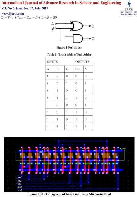
𝑇𝐶 = 𝑇𝑋𝑂𝑅 + 𝑇𝐴𝑁𝐷 + 𝑇𝑂𝑅= 𝐷 + 𝐷 + 𝐷 = 3𝐷Figure 1:Full adder
Table 1: Truth table of Full Adder
INPUTS OUTPUTS
A B Cin Cout S
0 0 0 0 0
0 0 1 0 1
0 1 0 0 1
0 1 1 1 0
1 0 0 0 1
1 0 1 1 0
1 1 0 1 0
1 1 1 1 1
131 |
P a g e
Figure 3: Full adder in Base case using DSCH2
III. FULL ADDER WITH NAND GATES
As mentioned earlier, a NAND gate is one of the universal gates and can be used to implement any logic design. The circuit of full adder using only NAND gates is shown in figure 5.Full adder is a simple 1 – bit adder. If we want to perform n – bit addition, then n number of 1 – bit full adders should be used in the form of a cascade connection. To construct a full adder circuit, we’ll need three inputs and two outputs. Since we’ll have both an input carry and an output carry, we’ll designate them as CIN and COUT. At the same time, we’ll use S to designate the final Sum output. The resulting truth table is shown to the rightif COUT may be either an AND or an OR function, depending on the value of A, and S is either an XOR or an XNOR, again depending on the value of A. Looking a little more closely, however, we can note that the S output is actually an XOR between the A input and the half-adder SUM output with B and CIN inputs. Also, the output carry will be true if any two or all three inputs are logic 1.What this suggests is also intuitively logical: we can use two half-adder circuits. The first will add A and B to produce a partial Sum, while the second will add CIN to that Sum to produce the final S output. If either half-adder produces a carry, there will be an output carry. Thus, COUT will be an OR function of the half-adder Carry outputs. The resulting full half-adder circuit is shown in figure 5
132 |
P a g e
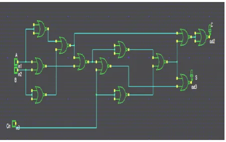
Figure 5:Full adder design with NAND gates using DSCH2
IV. FULL ADDER WITH NOR GATES
The NOR gate is a digital logic gate that implements logical NOR - it behaves according to the truth table to the right. A HIGH output (1) results if both the inputs to the gate are LOW (0); if one or both input is HIGH (1), a LOW output (0) results. NOR is the result of the negation of the OR operator. It can also be seen as an AND gate with all the inputs inverted. NOR is a functionally complete operation—NOR gates can be combined to generate any other logical function. it shares this property with the NAND gate. By contrast, the OR operator is monotonic as it can only change LOW to HIGH but not vice versa.In most, but not all, circuit implementations, the negation comes for free including CMOS and TTL. In such logic families, OR is the more complicated operation; it may use a NOR followed by a NOT. A significant exception is some forms of the domino logic family.
133 |
P a g e
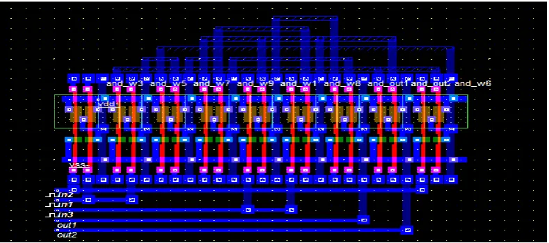
Figure 7:Stick diagram of Full adder with NOR gates in Microwind tool
Table 2:
V. RESULT
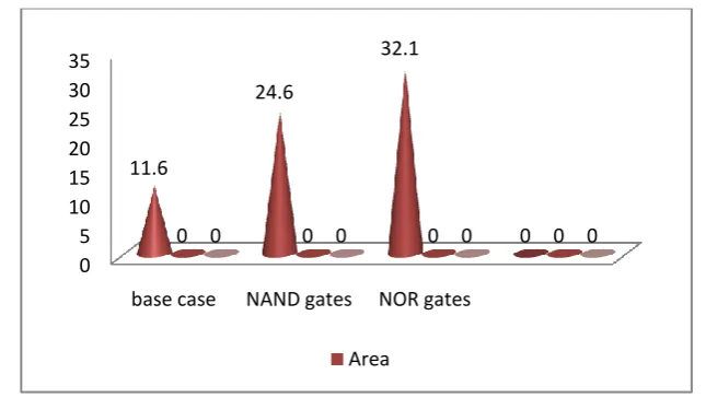
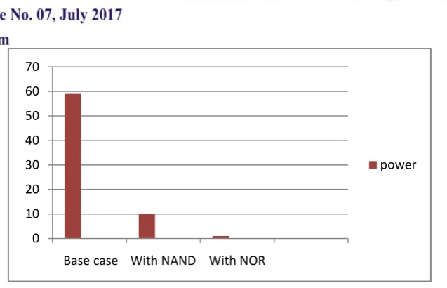
All three cases were designed using DSCH2 and simulation is carried in Microwind tool version 3.1 with 32 nano Meter technology implementing BSIM4 features .Our simulation result shows that NOR gate with 12 transistors consume very less power (1n W).NAND gate design consume 10 nW of power .Base case consume more power than NAND and NOR based full adder design .NOR based full adder requires more area and is two and half times to base case .Hence we conclude that where power is not prime important there Full adder with base case can be used and where power is given high priority and area is of least interest there Full adder with NAND gates can be used .
Figure 8: Comparison of area in all three cases
0 5 10 15 20 25 30 35
base case NAND gates NOR gates
11.6
24.6
32.1
0
0 0 0 0 0 0 0 0
Area
Input supply voltage
Area Power
dissipated
Number of transistors used
Full Adder 0.2V 11.6 𝜇𝑚2 0.059𝜇𝑊 5
Full Adder with NAND gates
0.2V 24.6 𝜇𝑚2 10𝑛𝑊 9
Full Adder with NOR gates
134 |
P a g e
Figure 9: Comparison of dissipated power in all three cases
VI. FUTURE SCOPE
In this paper a full adder is designed using NAND and NOR gates. Full adder design with NOR gates dissipates less power than base case and Full adder with NAND. To carry further work researchers can design full adder with 14 NOR gates and focus on minimizing leakage currents instead of reducing area .
REFERENCES
[1] S. Govindarajulu, T.Jayachandra Prasad, ―Design of High erformance Dynamic CMOS Circuits in Deep Submicron Technology‖, IJEST, vol.2, No.7, 2010, pp.2903- 2917.
[2] R. K. Krishnamurty, A. Alvandpour, V. De, and S. Borkar, ―High-performance and low- power challenges for sub-70 nm microprocessor circuits,‖in Proc. IEEE Custom Integrated Circuits Conf., May 2002, pp.125– 128.
[3] S.Govindarajulu, T.Jayachandra Prasad, ―Low power, Energy efficient Domino Logic Circuits‖, IJRTE, vol.2, No.7, Nov.2009, pp.30- 33, Academy Publishers, ACEEE, Finland.
[4] S. Govindarajulu, T. Jayachandra Prasad, ―Low-Power,High Performance Dual Threshold Voltage CMOS Domino Logic Circuits‖, published in ICRAES, 8th & 9th Jan’2010, pp-109- 117,KSR College of Engg., Tiruchengode, India.
[5] S.Govindarajulu, T.Jayachandra Prasad, ―Considerations of Performance Factors in CMOS Designs‖, ICED 2008, Dec.1- 3 ,Penang, Malaysia, IEEE Xplore.
[6] S.Govindarajulu, T.Jayachandra Prasad, ―,Energy efficient Reduced swing Domino Logic Circuits in 65nm Technology‖, IJEST, Vol. 2(6), 2010, pp.2248-2257.
[7] S.Govindarajulu, T.Jayachandra Prasad, ―,Temperature Variation Insensitivein Energy-efficient CMOS Circuits Design in 65 nm Technology‖, IJEST, Vol. 2(6), 2010, pp. 2140-2147.
[8] Microwind and Dsch v3.0 – Lite User’s Manual – Etienne Sicard.
[9] ―Fundamental of digital circuits‖ – A. Anand Kumar [10] ―CMOS Digital Integrated Circuits‖ – Sung-Mo Kang, Yusuf Leblebici.
0 10 20 30 40 50 60 70
Base case With NAND With NOR